
ADS1100
SBAS239 ≠ MAY 2002
www.ti.com
DESCRIPTION
The ADS1100 is a precision, continuously self-calibrating
Analog-to-Digital (A/D) converter with differential inputs and
up to 16 bits of resolution in a small SOT23-6 package.
Conversions are performed ratiometrically, using the power
supply as the reference voltage. The ADS1100 uses an
I
2
C-compatible serial interface and operates from a single
power supply ranging from 2.7V to 5.5V.
The ADS1100 can perform conversions at rates of 8, 16, 32,
or 128 samples per second. The onboard programmable-
gain amplifier, which offers gains of up to 8, allows smaller
signals to be measured with high resolution. In single-
conversion mode, the ADS1100 automatically powers down
after a conversion, greatly reducing current consumption
during idle periods.
The ADS1100 is designed for applications requiring high-
resolution measurement, where space and power consump-
tion are major considerations. Typical applications include
portable instrumentation, industrial process control and smart
transmitters.
FEATURES
q
COMPLETE DATA ACQUISITION SYSTEM IN A
TINY SOT23-6 PACKAGE
q
16-BITS NO MISSING CODES
q
INL: 0.0125% of FSR MAX
q
CONTINUOUS SELF-CALIBRATION
q
SINGLE-CYCLE CONVERSION
q
PROGRAMMABLE GAIN AMPLIFIER
GAIN = 1, 2, 4, OR 8
q
LOW NOISE: 4
µ
Vp-p
q
PROGRAMMABLE DATA RATE: 8SPS to 128SPS
q
INTERNAL SYSTEM CLOCK
q
I
2
C
TM
INTERFACE
q
POWER SUPPLY: 2.7V TO 5.5V
q
LOW CURRENT CONSUMPTION: 90
µ
A
Copyright © 2002, Texas Instruments Incorporated
Self-Calibrating, 16-Bit
ANALOG-TO-DIGITAL CONVERTER
Please be aware that an important notice concerning availability, standard warranty, and use in critical applications of
Texas Instruments semiconductor products and disclaimers thereto appears at the end of this data sheet.
APPLICATIONS
q
PORTABLE INSTRUMENTATION
q
INDUSTRIAL PROCESS CONTROL
q
SMART TRANSMITTERS
q
CONSUMER GOODS
q
FACTORY AUTOMATION
q
TEMPERATURE MEASUREMENT
A/D
Converter
I
2
C
Interface
Clock
Oscillator
V
IN+
V
IN≠
SCL
SDA
V
DD
GND
A = 1, 2, 4, or 8
PGA
BAAI
PRODUCTION DATA information is current as of publication date.
Products conform to specifications per the terms of Texas Instruments
standard warranty. Production processing does not necessarily include
testing of all parameters.
I
2
C is a registered trademark of Philips Incorporated.
ADS1100
2
SBAS239
www.ti.com
V
DD
to GND ........................................................................... ≠0.3V to +6V
Input Current ............................................................... 100mA, Momentary
Input Current ................................................................. 10mA, Continuous
Voltage to GND, V
IN
+, V
IN
≠ ........................................ ≠0.3V to V
DD
+ 0.3V
Voltage to GND, SDA, SCL ..................................................... ≠0.5V to 6V
Maximum Junction Temperature ................................................... +150
∞
C
Operating Temperature .................................................... ≠40
∞
C to +85
∞
C
Storage Temperature ...................................................... ≠60
∞
C to +150
∞
C
Lead Temperature (soldering, 10s) ............................................... +300
∞
C
NOTE: (1) Stresses above those listed under "Absolute Maximum Ratings" may
cause permanent damage to the device. Exposure to absolute maximum
conditions for extended periods may affect device reliability.
ABSOLUTE MAXIMUM RATINGS
ELECTROSTATIC
DISCHARGE SENSITIVITY
This integrated circuit can be damaged by ESD. Texas
Instruments recommends that all integrated circuits be handled
with appropriate precautions. Failure to observe proper han-
dling and installation procedures can cause damage.
ESD damage can range from subtle performance degrada-
tion to complete device failure. Precision integrated circuits
may be more susceptible to damage because very small
parametric changes could cause the device not to meet its
published specifications.
SPECIFIED
PACKAGE
TEMPERATURE
PACKAGE
ORDERING
TRANSPORT
PRODUCT
I
2
C ADDRESS
(1)
PACKAGE-LEAD
DESIGNATOR
(2)
RANGE
MARKING
NUMBER
MEDIA, QUANTITY
ADS1100
1001 000
SOT23-6
DBV
≠40
∞
C to +85
∞
C
BAAI
ADS1100IDBVT
Tape and Reel, 250
"
"
"
"
"
"
ADS1100IDBVR
Tape and Reel, 3000
NOTES: (1) Contact TI or your local sales representative for more information on the availability of other addresses. (2) For the most current specifications and
package information, refer to our web site at www.ti.com.
PACKAGE/ORDERING INFORMATION
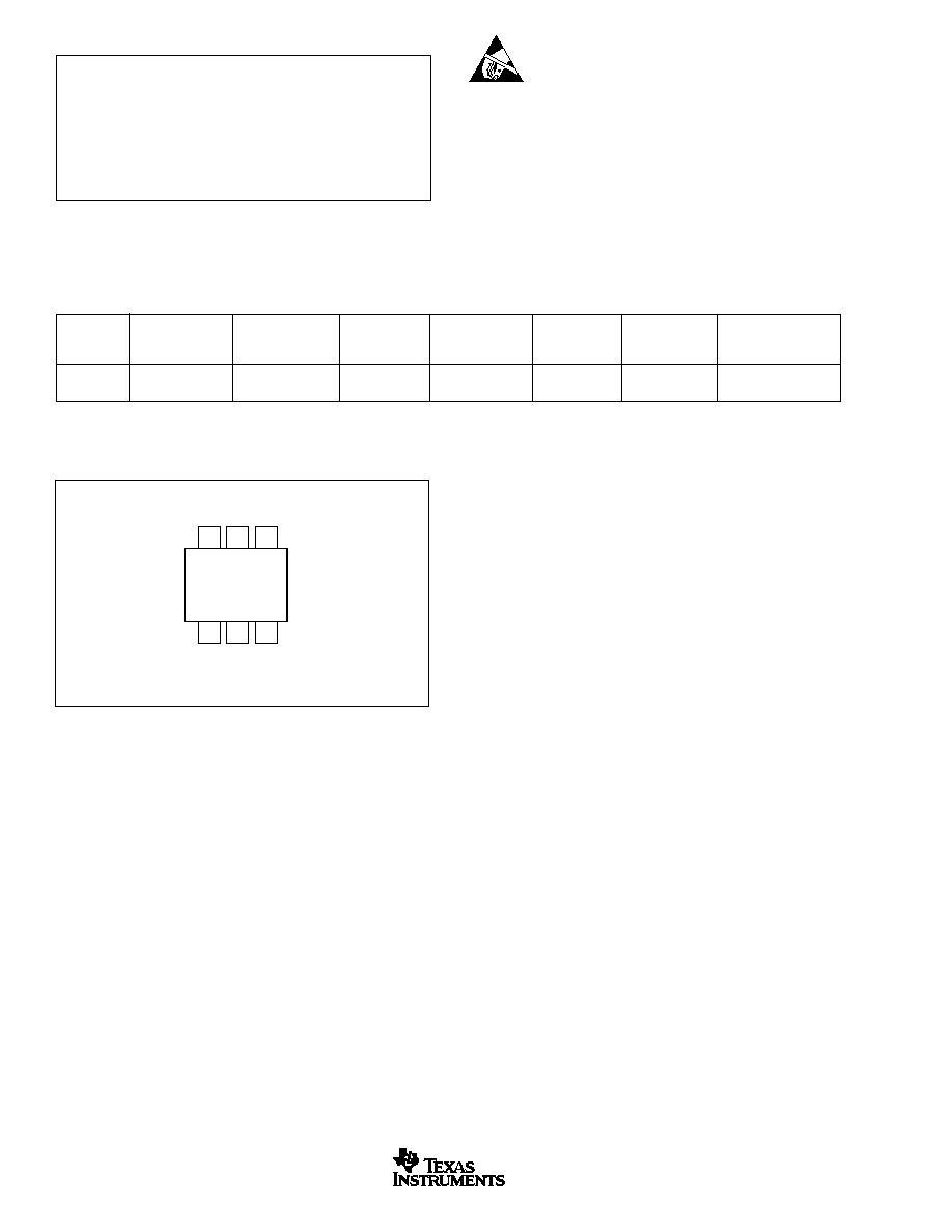
Top View
SOT
PIN CONFIGURATION
BAAI
1
2
3
6
5
4
V
IN+
GND SCL
V
IN≠
V
DD
SDA
NOTE: Marking text direction indicates pin 1.

ADS1100
3
SBAS239
www.ti.com
ADS1100
PARAMETER
CONDITIONS
MIN
TYP
MAX
UNITS
ANALOG INPUT
Full-Scale Input Voltage
(V
IN
+) ≠ (V
IN
≠)
±
V
DD
/PGA
V
Analog Input Voltage
V
IN
+, V
IN
≠ to GND
GND ≠ 0.2
V
DD
+ 0.2
V
Differential Input Impedance
2.4/PGA
M
Common-Mode Input Impedance
8
M
SYSTEM PERFORMANCE
Resolution and No Missing Codes
DR = 00
12
12
Bits
DR = 01
14
14
Bits
DR = 10
15
15
Bits
DR = 11
16
16
Bits
Conversion Rate
DR = 00
104
128
184
SPS
DR = 01
26
32
46
SPS
DR = 10
13
16
23
SPS
DR = 11
6.5
8
11.5
SPS
Output Noise
See Typical Characteristic Curves
Integral Nonlinearity
DR = 11, PGA = 1, End Point Fit
(1)
±
0.003
±
0.0125
% of FSR
(2)
Offset Error
±
2.5/PGA
±
5/PGA
mV
Offset Drift
PGA = 1
1.5
8
µ
V/
∞
C
PGA = 2
1.0
4
µ
V/
∞
C
PGA = 4
0.7
2
µ
V/
∞
C
PGA = 8
0.6
2
µ
V/
∞
C
Gain Error
0.01
0.1
%
Gain Error Drift
2
ppm/
∞
C
Common-Mode Rejection
At DC, PGA = 8
94
100
dB
At DC, PGA = 1
85
dB
DIGITAL INPUT/OUTPUT
Logic Level
V
IH
0.7 ∑ V
DD
6
V
V
IL
GND ≠ 0.5
0.3 ∑ V
DD
V
V
OL
I
OL
= 3mA
GND
0.4
V
Input Leakage
I
IH
V
IH
= 5.5V
10
µ
A
I
IL
V
IL
= GND
≠10
µ
A
POWER-SUPPLY REQUIREMENTS
Power-Supply Voltage
V
DD
2.7
5.5
V
Supply Current
Power Down
0.05
2
µ
A
Active Mode
90
150
µ
A
Power Dissipation
V
DD
= 5.0V
450
750
µ
W
V
DD
= 3.0V
210
µ
W
NOTES: (1) 99% of full-scale. (2) FSR = Full-Scale Range = 2 ∑ V
DD
/PGA.
ELECTRICAL CHARACTERISTICS
All specifications at ≠40
∞
C to +85
∞
C, V
DD
= 5V, GND = 0V, all PGAs, unless otherwise noted.

ADS1100
4
SBAS239
www.ti.com
TYPICAL CHARACTERISTICS
At T
A
= 25
∞
C, V
DD
= 5V, unless otherwise noted.
120
100
80
60
40
I
VDD
(
µ
A)
SUPPLY CURRENT vs TEMPERATURE
≠60
≠40
≠20
0
20
40
60
80
100
120
140
Temperature (
∞
C)
V
DD
= 5V
V
DD
= 2.7V
SUPPLY CURRENT vs I
2
C BUS FREQUENCY
250
225
200
175
150
125
100
75
50
10
100
1k
10k
I
2
C Bus Frequency (kHz)
I
VDD
(
µ
A)
125
∞
C
25
∞
C
≠40
∞
C
2.0
1.0
0.0
≠1.0
≠2.0
Of
fset Error (mV)
OFFSET ERROR vs TEMPERATURE
≠60
≠40
≠20
0
20
40
60
80
100
120
140
Temperature (
∞
C)
PGA = 8
PGA = 4
PGA = 2
PGA = 1
V
DD
= 5V
2.0
1.0
0.0
≠1.0
≠2.0
Of
fset Error (mV)
OFFSET ERROR vs TEMPERATURE
≠60
≠40
≠20
0
20
40
60
80
100
120
140
Temperature (
∞
C)
PGA = 8
PGA = 4
PGA = 2
PGA = 1
V
DD
= 2.7V
0.04
0.03
0.02
0.01
0.00
≠0.01
≠0.02
≠0.03
≠0.04
Gain Error (%)
GAIN ERROR vs TEMPERATURE
≠60
≠40
≠20
0
20
40
60
80
100
120
140
Temperature (
∞
C)
PGA = 8
PGA = 4
PGA = 1
PGA = 2
V
DD
= 5V
0.010
0.005
0.000
≠0.005
≠0.010
≠0.015
≠0.020
Gain Error (%)
GAIN ERROR vs TEMPERATURE
≠60
≠40
≠20
0
20
40
60
80
100
120
140
Temperature (
∞
C)
PGA = 8
PGA = 4
PGA = 1
PGA = 2
V
DD
= 2.7V

ADS1100
5
SBAS239
www.ti.com
TYPICAL CHARACTERISTICS
At T
A
= 25
∞
C, V
DD
= 5V, unless otherwise noted.
TOTAL ERROR vs INPUT SIGNAL
T
otal Error (mV)
0.0
≠0.5
≠1.0
≠1.5
≠2.0
≠2.5
≠100
≠75
≠50
≠25
0
25
50
75
100
Input Signal (% of Full-Scale)
PGA = 8
PGA = 4
PGA = 2
PGA = 1
Data Rate = 8SPS
PGA = 8
PGA = 4
PGA = 2
PGA = 1
INTEGRAL NONLINEARITY vs
SUPPLY VOLTAGE
0.016
0.014
0.012
0.010
0.008
0.006
0.004
0.002
0.000
Integral Nonlinearity (% of FSR)
2.5
3.0
3.5
4.0
4.5
5.0
5.5
V
DD
(V)
V
DD
= 2.7V
V
DD
= 5V
V
DD
= 3.5V
0.05
0.04
0.03
0.02
0.01
0.00
Integral Nonlinearity (% of FSR)
INTEGRAL NONLINEARITY vs TEMPERATURE
≠60
≠40
≠20
0
20
40
60
80
100
120
140
Temperature (
∞
C)
PGA =1
20
15
10
5
0
Noise (p-p, % of LSB)
NOISE vs INPUT SIGNAL
0
20
40
60
80
100
Input Signal (% of Full-Scale)
PGA = 8
PGA = 4
PGA = 2
PGA = 1
Data Rate = 8SPS
PGA = 8
PGA = 4
PGA = 2
PGA = 1
NOISE vs SUPPLY VOLTAGE
30
25
20
15
10
5
0
Noise (p-p, % of LSB)
2.5
3.0
3.5
4.0
4.5
5.0
5.5
V
DD
(V)
Data Rate = 8SPS
NOISE vs TEMPERATURE
25
20
15
10
5
Noise (p-p, % of LSB)
≠60
≠40
≠20
0
20
40
60
80
100
120
140
Temperature (
∞
C)
Data Rate = 8SPS
PGA = 8