 | –≠–ª–µ–∫—Ç—Ä–æ–Ω–Ω—ã–π –∫–æ–º–ø–æ–Ω–µ–Ω—Ç: ADS1112 | –°–∫–∞—á–∞—Ç—å:  PDF PDF  ZIP ZIP |
Document Outline
- FEATURES
- APPLICATIONS
- DESCRIPTION
- ABSOLUTE MAXIMUM RATINGS(
- PACKAGE/ORDERING INFORMATION
- Terminal Functions
- ELECTRICAL CHARACTERISTICS
- TYPICAL CHARACTERISTICS
- THEORY OF OPERATION
- ANALOG-TO-DIGITAL CONVERTER
- MULTIPLEXER
- VOLTAGE REFERENCE
- OUTPUT CODE CALCULATION
- SELF-CALIBRATION
- CLOCK OSCILLATOR
- INPUT IMPEDANCE
- ALIASING
- USING THE ADS1112
- OPERATING MODES
- RESET AND POWER-UP
- I2C INTERFACE
- SERIAL BUS ADDRESS
- I2C GENERAL CALL
- I2C DATA RATES
- REGISTERS
- OUTPUT REGISTER
- CONFIGURATION REGISTER
- Bit 7: ST/DRDY\
- Bits 6-5: INP
- Bit 4: SC
- Bits 3-2: DR
- Bits 1-0: PGA
- READING FROM THE ADS1112
- WRITING TO THE ADS1112
- APPLICATIONS INFORMATION
- BASIC CONNECTIONS
- CONNECTING MULTIPLE DEVICES
- USING GPIO PORTS FOR I2C
- SINGLE-ENDED INPUTS
- LOW-SIDE CURRENT MONITOR

FEATURES
D
COMPLETE DATA ACQUISITION SYSTEM IN
THE MSOP-10 AND LEADLESS QFN-STYLE
PACKAGES
D
MEASUREMENTS FROM TWO DIFFERENTIAL
CHANNELS OR THREE SINGLE-ENDED
CHANNELS
D
I
2
C
INTERFACE--EIGHT ADDRESSES PIN-
SELECTABLE
D
ONBOARD REFERENCE:
Accuracy: 2.048V
±
0.05%
Drift: 5ppm/
∞
C
D
ONBOARD PGA
D
ONBOARD OSCILLATOR
D
16 BITS, NO MISSING CODES
D
INL: 0.01% of FSR max
D
CONTINUOUS SELF-CALIBRATION
D
SINGLE-CYCLE CONVERSION
D
PROGRAMMABLE DATA RATE: 15SPS to
240SPS
D
POWER SUPPLY: 2.7V to 5.5V
D
LOW CURRENT CONSUMPTION: 240
µ
A
APPLICATIONS
D
PORTABLE INSTRUMENTATION
D
INDUSTRIAL PROCESS CONTROL
D
SMART TRANSMITTERS
D
CONSUMER GOODS
D
FACTORY AUTOMATION
D
TEMPERATURE MEASUREMENT
DESCRIPTION
The ADS1112 is a precision, continuously self-calibrating
Analog-to-Digital (A/D) converter with two differential or three
single-ended channels and up to 16 bits of resolution in the
small MSOP-10 and leadless QFN-style (small-outline,
no-lead) packages. The onboard 2.048V reference provides
an input range of
±
2.048V differentially. The ADS1112 uses
an I
2
C-compatible serial interface and has two address pins
that allow a user to select one of the eight I
2
C Slave
addresses. The ADS1112 operates from a single power
supply ranging from 2.7V to 5.5V.
The ADS1112 can perform conversions at rates of 15, 30, 60,
or 240 samples per second (SPS). The onboard
programmable gain amplifier (PGA), which offers gains of up
to eight, allows smaller signals to be measured with high
resolution. In single-conversion mode, the ADS1112
automatically powers down after a conversion, greatly
reducing current consumption during idle periods.
The ADS1112 is designed for applications requiring
high-resolution measurement, where space and power
consumption are major considerations. Typical applications
include portable instrumentation, industrial process control,
and smart transmitters.
All trademarks are the property of their respective owners.
ADS1112
SBAS282D - JUNE 2003 - REVISED MARCH 2004
16-Bit Analog-to-Digital Converter with
Input Multiplexer and Onboard Reference
www.ti.com
Copyright
2003-2004, Texas Instruments Incorporated
Please be aware that an important notice concerning availability, standard warranty, and use in critical applications of Texas Instruments
semiconductor products and disclaimers thereto appears at the end of this data sheet.
PRODUCTION DATA information is current as of publication date. Products
conform to specifications per the terms of Texas Instruments standard warranty.
Production processing does not necessarily include testing of all parameters.

ADS1112
SBAS282D - JUNE 2003 - REVISED MARCH 2004
www.ti.com
2
ABSOLUTE MAXIMUM RATINGS
(1)
VDD to GND
-0.3V to +6V
Input Current
100mA, Momentary
Input Current
10mA, Continuous
Analog Inputs, A0, A1, Voltage to GND
-0.3V to VDD + 0.3V
SDA, SCL Voltage to GND
-0.5V to 6V
Maximum Junction Temperature
+150
∞
C
Operating Temperature Range
-40
∞
C to +125
∞
C
Storage Temperature Range
-60
∞
C to +150
∞
C
Lead Temperature (soldering, 10s)
+300
∞
C
(1) Stresses above those listed under Absolute Maximum Ratings
may cause permanent damage to the device. Exposure to
absolute maximum conditions for extended periods may affect
device reliability.
This integrated circuit can be damaged by ESD.
Texas Instruments recommends that all
integrated circuits be handled with appropriate
precautions. Failure to observe proper handling and
installation procedures can cause damage.
ESD damage can range from subtle performance degradation
to complete device failure. Precision integrated circuits may
be more susceptible to damage because very small
parametric changes could cause the device not to meet its
published specifications.
PACKAGE/ORDERING INFORMATION
PRODUCT
PACKAGE-LEAD
PACKAGE
DESIGNATOR(1)
SPECIFIED
TEMPERATURE
RANGE
PACKAGE
MARKING
ORDERING NUMBER
TRANSPORT MEDIA,
QUANTITY
ADS1112
MSOP-10
DGS
-40
∞
C to +85
∞
C
BHU
ADS1112IDGST
Tape and Reel, 250
ADS1112
MSOP-10
DGS
-40
∞
C to +85
∞
C
BHU
ADS1112IDGSR
Tape and Reel, 2500
ADS1112
SON-10
DRC
-40
∞
C to +85
∞
C
BHV
ADS1112IDRCT
Tape and Reel, 250
ADS1112
SON-10
DRC
-40
∞
C to +85
∞
C
BHV
ADS1112IDRCR
Tape and Reel, 3000
(1) For the most current specification and package information, refer to our web site at www.ti.com.
Top View
MSOP-10
Top View
SON-10
Terminal Functions
TERMINAL
NAME
NO.
DESCRIPTION
AIN0
1
Differential Channel 1; Positive Input
Single
-
ended Channel 1 Input
AIN1
2
Differential Channel 1; Negative Input
Single
-
ended Channel 2 Input
GND
3
Ground
AIN2
4
Differential Channel 2; Positive Input
Single
-
ended Channel 3 Input
AIN3
5
Differential Channel 2; Negative Input
Single
-
ended Common Input
VDD
6
Power Supply: 2.7V to 5.5V
SDA
7
Serial Data: Transmits and receives
data
SCL
8
Serial Clock Input: Clocks output
data on SDA
A0
9
I2C Slave Address Select
A1
10
I2C Slave Address Select

ADS1112
SBAS282D - JUNE 2003 - REVISED MARCH 2004
www.ti.com
3
ELECTRICAL CHARACTERISTICS
All specifications at -40
∞
C to +85
∞
C, VDD = 5V, and all PGAs, unless otherwise noted.
ADS1112
PARAMETER
CONDITIONS
MIN
TYP
MAX
UNIT
ANALOG INPUT
Full-Scale Input Voltage
(VIN+) - (VIN-)
±
2.048/PGA
V
Analog Input Voltage
VIN+ to GND or VIN- to GND
GND - 0.2
VDD + 0.2
V
Differential Input Impedance
2.8/PGA
M
Common-Mode Input Impedance
PGA = 1
3.5
M
PGA = 2
3.5
M
PGA = 4
1.8
M
PGA = 8
0.9
M
SYSTEM PERFORMANCE
Resolution and No Missing Codes
DR = 00
12
12
Bits
Resolution and No Missing Codes
DR = 01
14
14
Bits
DR = 10
15
15
Bits
DR = 11
16
16
Bits
Data Rate
DR = 00
180
240
308
SPS
Data Rate
DR = 01
45
60
77
SPS
DR = 10
22
30
39
SPS
DR = 11
11
15
20
SPS
Output Noise
See Typical Characteristic Curves
Integral Nonlinearity
DR = 11, PGA = 1, End Point Fit(1)
±
0.004
±
0.010
%
of FSR
(2)
Offset Error
PGA = 1
1.2
8
mV
Offset Error
PGA = 2
0.7
4
mV
PGA = 4
0.5
2.5
mV
PGA = 8
0.4
1.5
mV
Offset Drift
PGA = 1
1.2
µ
V/
∞
C
Offset Drift
PGA = 2
0.6
µ
V/
∞
C
PGA = 4
0.3
µ
V/
∞
C
PGA = 8
0.3
µ
V/
∞
C
Offset vs VDD
PGA = 1
800
µ
V/V
Offset vs VDD
PGA = 2
400
µ
V/V
PGA = 4
200
µ
V/V
PGA = 8
150
µ
V/V
Channel Offset Match
Match between any two channels
30
µ
V
Gain Error(3)
0.05
0.40
%
PGA Gain Error Match(3)
Match between any two PGA gains
0.02
0.10
%
Gain Error Drift(3)
5
40
ppm/
∞
C
Gain vs VDD
80
ppm/V
Channel Gain Match
Match between any two channels
0.01
%
Common-Mode Rejection
At DC and PGA = 8
95
105
dB
Common-Mode Rejection
At DC and PGA = 1
100
dB
DIGITAL INPUT/OUTPUT
Logic Level
VIH
0.7
∑
VDD
6
V
VIL
GND - 0.5
0.3
∑
VDD
V
VOL
IOL = 3mA
GND
0.4
V
Input Leakage
IH
VIH = 5.5V
10
µ
A
IL
VIL = GND
-10
µ
A
POWER-SUPPLY REQUIREMENTS
Power-Supply Voltage
VDD
2.7
5.5
V
Supply Current
Power-Down
0.05
2
µ
A
Supply Current
Active Mode
240
350
µ
A
Power Dissipation
VDD = 5.0V
1.2
1.75
mW
Power Dissipation
VDD = 3.0V
0.675
mW
(1) 99% of full-scale.
(2) FSR = full-scale range = 2
◊
2.048V/PGA = 4.096V/PGA.
(3) Includes all errors from onboard PGA and reference.
ADS1112
SBAS282D - JUNE 2003 - REVISED MARCH 2004
www.ti.com
4
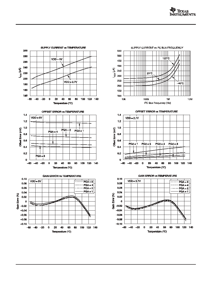
TYPICAL CHARACTERISTICS
At TA = 25
∞
C and VDD = 5V, unless otherwise noted.

ADS1112
SBAS282D - JUNE 2003 - REVISED MARCH 2004
www.ti.com
5
TYPICAL CHARACTERISTICS (continued)
At TA = 25
∞
C and VDD = 5V, unless otherwise noted.