Document Outline
- FEATURES
- APPLICATIONS
- DESCRIPTION
- ORDERING INFORMATION
- ABSOLUTE MAXIMUM RATINGS
- RECOMMENDED OPERATING CONDITIONS
- DISSIPATION RATING TABLE
- ELECTRICAL CHARACTERISTICS
- EQUIVALENT INPUT CIRCUIT
- PIN ASSIGNMENTS
- Terminal Functions
- PARAMETER MEASUREMENT INFORMATION
- TIMING CHARACTERISTICS: MODE 0
- TIMING CHARACTERISTICS: MODE 1
- TIMING CHARACTERISTICS: MODE 2
- TIMING CHARACTERISTICS: MODE 3
- TYPICAL CHARACTERISTICS
- GENERAL DESCRIPTION
- THEORY OF OPERATION
- ANALOG INPUT STAGE
- DIGITAL OUTPUT
- DIGITAL INTERFACE
- MODES OF OPERATION
- Mode 0
- Mode 1
- Mode 2
- Mode 3
- FILTER USAGE
- APPLICATIONS
- LAYOUT CONSIDERATIONS
- Power Supplies
- Grounding
- Decoupling
SBAS318 - JUNE 2004
Motor Control Current Measurement
1 Bit, 10MHz, 2nd Order, Delta Sigma Modulator
ADS1203
FEATURES
D
16-Bit Resolution
D
14-Bit Linearity
D
±
250mV Input Range with Single +5V Supply
D
1% Internal Reference Voltage
D
1% Gain Error
D
Flexible Serial Interface with Four Different
Modes
D
Implemented Twinned Binary Coding as
Split-Phase or Manchester Coding for
One-Line Interfacing
D
Operating Temperature Range:
-40
∞
C to +85
∞
C
APPLICATIONS
D
Motor Control
D
Current Measurement
D
Industrial Process Control
D
Instrumentation
D
Smart Transmitters
D
Portable Instruments
D
Weight Scales
D
Pressure Transducers
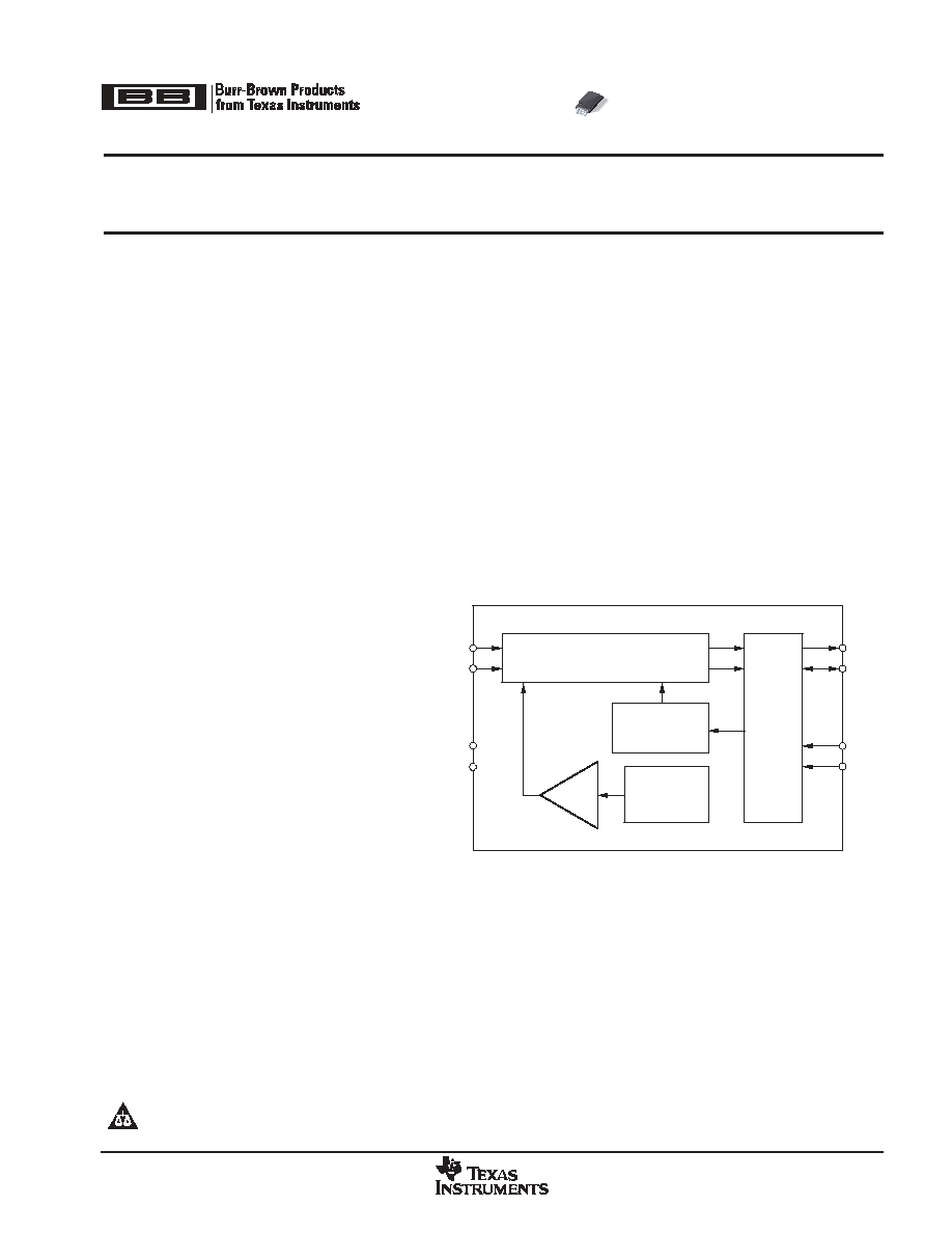
DESCRIPTION
The ADS1203 is a delta-sigma (
) modulator with a
95dB dynamic range, operating from a single +5V
supply. The differential inputs are ideal for direct
connection to transducers or low-level signals. With the
appropriate digital filter and modulator rate, the device
can be used to achieve 16-bit analog-to-digital (A/D)
conversion with no missing codes. An effective
resolution of 14 bits or SNR of 85dB (typical) can be
maintained with a digital filter bandwidth of 40kHz at a
modulator rate of 10MHz. The ADS1203 is designed for
use in medium- to high-resolution measurement
applications including current measurements, smart
transmitters, industrial process control, weigh scales,
chromatography, and portable instrumentation. It is
available in an 8-lead TSSOP package. A 16-pin QFN
(3x3) package will be available soon.
www.ti.com
Copyright
2004, Texas Instruments Incorporated
Please be aware that an important notice concerning availability, standard warranty, and use in critical applications of Texas Instruments
semiconductor products and disclaimers thereto appears at the end of this data sheet.
All trademarks are the property of their respective owners.
PRODUCTION DATA information is current as of publication date. Products
conform to specifications per the terms of Texas Instruments standard warranty.
Production processing does not necessarily include testing of all parameters.
Buffer
Reference
Voltage
2.5V
2nd-Order
Modulator
RC Oscillator
20MHz
Interface
Circuit
MDAT
MCLK
M0
M1
V
IN
+
V
IN
-
V
DD
GND

ADS1203
SBAS318 - JUNE 2004
www.ti.com
2
This integrated circuit can be damaged by ESD. Texas Instruments recommends that all integrated circuits be handled with appropriate
precautions. Failure to observe proper handling and installation procedures can cause damage.
ESD damage can range from subtle performance degradation to complete device failure. Precision integrated circuits may be more susceptible to
damage because very small parametric changes could cause the device not to meet its published specifications.
ORDERING INFORMATION
PRODUCT
MAXIMUM
INTEGRAL
LINEARITY
ERROR
(LSB)
MAXIMUM
GAIN
ERROR (%)
PACKAGE-
LEAD
PACKAGE
DESIGNATOR(1)
SPECIFIED
TEMPERATURE
RANGE
PACKAGE
MARKING
ORDERING
NUMBER
TRANSPORT
MEDIA, QUANTITY
ADS1203(2)
±
3
±
1
TSSOP-8
PW
-40
∞
C to +85
∞
C
AZ1203
ADS1203IPWT
Tape and Reel, 250
ADS1203(2)
±
3
±
1
TSSOP-8
PW
-40
∞
C to +85
∞
C
AZ1203
ADS1203IPWR
Tape and Reel, 2000
(1) For the most current specification and package information, refer to our web site at www.ti.com.
(2) 16-pin QFN (3x3) package available soon.
ABSOLUTE MAXIMUM RATINGS
over operating free-air temperature range unless otherwise noted(1)
ADS1203
UNIT
Supply voltage, GND to VDD
-0.3 to +6
V
Analog input voltage range
GND - 0.4 to VDD + 0.3
V
Digital input voltage range
GND - 0.3 to VDD + 0.3
V
Power Dissipation
0.25
W
Operating Virtual Junction Temperature Range, TJ
-40 to +150
∞
C
Operating Free-Air Temperature Range, TA
-40 to +85
∞
C
Storage Temperature Range, TSTG
-65 to +150
∞
C
Lead Temperature (1.6mm or 1/16
from case for 10s)
+260
∞
C
(1) Stresses beyond those listed under Absolute Maximum Ratings may cause permanent damage to the device. These are stress ratings only, and
functional operation of the device at these or any other conditions beyond those indicated under Recommended Operating Conditions is not
implied. Exposure to absolute-maximum-rated conditions for extended periods may affect device reliability.
RECOMMENDED OPERATING CONDITIONS
PARAMETER
MIN
NOM
MAX
UNIT
Supply Voltage, VDD
4.5
5.0
5.5
V
Analog Input Voltage
-250
+250
mV
Operating Common-Mode Signal
0
+5
V
External Clock(1)
16
20
24
MHz
Operating Junction Temperature Range
-40
+105
∞
C
(1) With reduced accuracy, clock can go from 1MHz up to 32MHz; see Typical Characteristic curves.
DISSIPATION RATING TABLE
PACKAGE
TA
25
∞
C
POWER RATING
DERATING FACTOR
ABOVE TA = 25
∞
C(1)
TA = 70
∞
C
POWER RATING
TA = 85
∞
C
POWER RATING
TSSOP-8
483.6mW
3.868mW/
∞
C
309.5mW
251.4W
(1) This is the inverse of the traditional junction-to-ambient thermal resistance (R
q
JA). Thermal resistances are not production tested and are for
informational purposes only.

ADS1203
SBAS318 - JUNE 2004
www.ti.com
3
ELECTRICAL CHARACTERISTICS
Over recommended operating free-air temperature range at -40
∞
C to +85
∞
C, VDD = +5V, VIN+ = -250mV to +250mV, VIN- = 0V, Mode 3,
MCLK input = 20MHz, and 16-bit Sinc3 filter, with OSR = 256, unless otherwise noted.
ADS1203IPW
PARAMETER
TEST CONDITIONS
MIN
TYP(1)
MAX
UNITS
Resolution
16
Bits
DC Accuracy
INL
Integral linearity error(2)
±
1
±
3
LSB
INL
Integral linearity error(2)
0.001
0.005
%
DNL
Differential nonlinearity(3)
±
1
LSB
VOS
Input offset
-220
±
1000
µ
V
TCVOS
Input offset drift
3.5
8
µ
V/
∞
C
GERR
Gain error(4)
-0.2
±
1
%
TCGERR
Gain error drift
20
ppm/
∞
C
PSRR
Power-supply rejection ratio
4.75V < VDD < 5.25V
80
dB
Analog Input
FSR
Full-scale differential range
(VIN+) - (VIN-)
±
320
mV
Operating common-mode signal(3)
-0.1
5
V
Input capacitance
Common-mode
3
pF
Input leakage current
±
1
nA
Differential input resistance
Equivalent
28
k
Differential input capacitance
5
pF
CMRR
Common-mode rejection ratio
At DC
92
dB
CMRR
Common-mode rejection ratio
VIN = 0V to 5V at 50kHz
105
dB
Internal Voltage Reference
VOUT
Reference voltage output
Scale to 320mV
2.475
2.5
2.525
V
Accuracy
Scale to 320mV
±
1
%
dVOUT/dT
Reference temperature drift
±
20
ppm/
∞
C
PSRR
Power-supply rejection ratio
80
dB
Startup time
to 0.1% at CL = 0
0.1
ms
Internal Clock for Modes 0, 1, and 2
Clock frequency
9
10
11
MHz
External Clock for Mode 3
Clock frequency(5)
16
20
24
MHz
AC Accuracy
SINAD
Signal-to-noise + distortion
VIN =
±
250mVPP at 5kHz
82.5
85
dB
SNR
Signal-to-noise ratio
VIN =
±
250mVPP at 5kHz
83
85
dB
THD
Total harmonic distortion
VIN =
±
250mVPP at 5kHz
-95
-88
dB
SFDR
Spurious-free dynamic range
VIN =
±
250mVPP at 5kHz
90
95
dB
(1) All typical values are at TA = +25
∞
C.
(2) Integral nonlinearity is defined as the maximum deviation of the line through the end points of the specified input range of the transfer curve
for VIN+ = -250mV to +250mV, expressed either as the number of LSBs or as a percent of measured input range (500mV).
(3) Ensured by design.
(4) Maximum values, including temperature drift, are ensured over the full specified temperature range.
(5) With reduced accuracy, minimum clock can go from 1MHz up to 32MHz.
ADS1203
SBAS318 - JUNE 2004
www.ti.com
4
ELECTRICAL CHARACTERISTICS (continued)
Over recommended operating free-air temperature range at -40
∞
C to +85
∞
C, VDD = +5V, VIN+ = -250mV to +250mV, VIN- = 0V, Mode 3,
MCLK input = 20MHz, and 16-bit Sinc3 filter, with OSR = 256, unless otherwise noted.
PARAMETER
UNITS
ADS1203IPW
TEST CONDITIONS
PARAMETER
UNITS
MAX
TYP(1)
MIN
TEST CONDITIONS
Digital Input
Logic family
CMOS with Schmitt Trigger
VIH
High-level input voltage
0.7
◊
VDD
VDD + 0.3
V
VIL
Low-level input voltage
-0.3
0.3
◊
VDD
V
IIH
High-level Input current
VI = VDD or GND
50
nA
IIL
Low-level Input current
VI = VDD or GND
-50
nA
CI
Input capacitance
5
pF
Digital Output
VOH
High-level digital output
VDD = 5V, IO = -5mA
4.6
V
VOH
High-level digital output
VDD = 5V, IO = -15mA
3.9
V
VOL
Low-level digital output
VDD = 5V, IO = 5mA
0.4
V
VOL
Low-level digital output
VDD = 5V, IO = 15mA
1.1
V
CO
Output capacitance
5
pF
CL
Load capacitance
30
pF
Power Supply
VDD
Supply voltage
4.5
5
5.5
V
ICC
Operating supply current
Mode 0
8.4
9.8
mA
ICC
Operating supply current
Mode 3
6.7
7.8
mA
Power dissipation
Mode 0
42
49
mW
Power dissipation
Mode 3
33.5
39
mW
Operating Temperature Range
-40
+85
∞
C
(1) All typical values are at TA = +25
∞
C.
(2) Integral nonlinearity is defined as the maximum deviation of the line through the end points of the specified input range of the transfer curve
for VIN+ = -250mV to +250mV, expressed either as the number of LSBs or as a percent of measured input range (500mV).
(3) Ensured by design.
(4) Maximum values, including temperature drift, are ensured over the full specified temperature range.
(5) With reduced accuracy, minimum clock can go from 1MHz up to 32MHz.
ADS1203
SBAS318 - JUNE 2004
www.ti.com
5
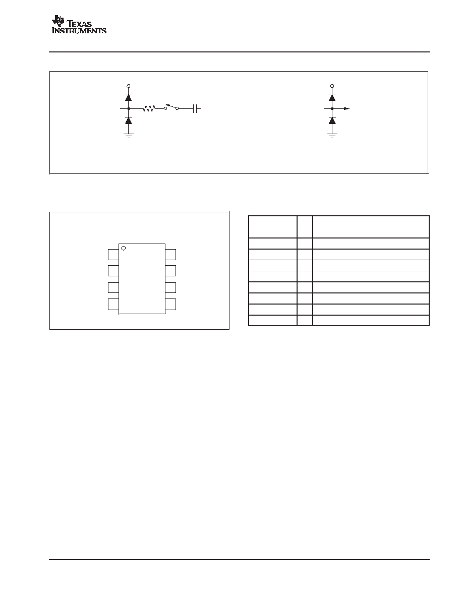
EQUIVALENT INPUT CIRCUIT
R
ON
= 350
C
(SAMPLE)
= 5pF
V
DD
V
DD
D
IN
GND
GND
A
IN
Diode Turn-on Voltage: 0.4V
Equivalent Analog Input Circuit
Equivalent Digital Input Circuit
PIN ASSIGNMENTS
TSSOP PACKAGE
(TOP VIEW)
1
2
3
4
8
7
6
5
M0
V
IN
+
V
IN
-
M1
V
DD
MCLK
MDAT
GND
ADS1203
Terminal Functions
TERMINAL
NAME
NO.
I/O
DESCRIPTION
M0
1
I
Mode input
VIN+
2
AI
Noninverting analog input
VIN-
3
AI
Inverting analog input
M1
4
I
Mode input
GND
5
P
Power supply ground
MDAT
6
O
Modulator data output
MCLK
7
I/O
Modulator clock input or output
VDD
8
P
Power supply: +5V nominal
NOTE: AI = analog input, AO = analog output, I = input, O = output,
P = power supply.