
SBAS311 - MARCH 2004
Low Power, Synchronous
Voltage to Frequency Converter
ADS1206
ADS1207
FEATURES
D
Syncronous Operation
D
Frequency Set By External Clock
D
Maximum Input Frequency:
- 1MHz for ADS1206
- 4MHz for ADS1207
D
Selectable High-Impedance Buffered Input
D
2% Internal, 2.5V Reference Voltage
D
High-Current Output Driver
D
Power Supply 3.3V or 5V
D
Low Power : 3mW (typ)
D
Alternate Source for AD7740
D
-40
�
C to +85
�
C Operating Temperature Range
APPLICATIONS
D
Galvanic Isolation Measurement
D
High Voltage Measurement
D
Low-Cost Analog-to-Digital Conversion
D
Motor Control
D
Industrial Process Control
D
Instrumentation
D
Smart Transmitters
D
Portable Instruments
DESCRIPTION
The ADS1206 and ADS1207 are a low-cost,
high-performance, synchronous voltage-to-frequency
converters (VFC). Both devices can operate from a single
3.0V to 3.6V or 4.5V to 5.5V power supply, consuming only
1mA. The output signal is synchronous with the input
clock, CLKIN. The clock input is TTL- and CMOS-
compatible and the onboard clock generator can also
accept an external crystal or resonator. The maximum
input clock frequency for the ADS1206 is 1MHz and for the
ADS1207 is 4MHz. The clock divider on the ADS1207
scales the input frequency to 2MHZ, which permits the
core to operate at the higher rate. The high-impedance
input is ideal for direct connection to high-impedance
transducers or high-voltage resistive dividers. Counting
output pulses over a 4ms period results in an effective
12-bit resolution for the ADS1206 using a 1MHz input
clock. For the ADS1207 using a 4MHz input clock, the
same result occurs over a 2ms period. Both devices are
designed for use in medium-resolution measurements.
They are available in an 8-lead VSSOP package.
1k
Reference
Voltage
2.5V
Modulator
-
2
Buffer
x1
REFIN/OUT
CLKOUT
ADS1207
Only
CLKIN
FOUT
VIN
BUF
PRODUCT PREVIEW
www.ti.com
Copyright
2004, Texas Instruments Incorporated
Please be aware that an important notice concerning availability, standard warranty, and use in critical applications of Texas Instruments
semiconductor products and disclaimers thereto appears at the end of this data sheet.
PRODUCT PREVIEW information concerns products in the formative or design
phase of development. Characteristic data and other specifications are design
goals. Texas Instruments reserves the right to change or discontinue these
products without notice.
All trademarks are the property of their respective owners.

ADS1206
ADS1207
SBAS311 - MARCH 2004
www.ti.com
2
This integrated circuit can be damaged by ESD. Texas Instruments recommends that all integrated circuits be handled with appropriate
precautions. Failure to observe proper handling and installation procedures can cause damage.
ESD damage can range from subtle performance degradation to complete device failure. Precision integrated circuits may be more susceptible to
damage because very small parametric changes could cause the device not to meet its published specifications.
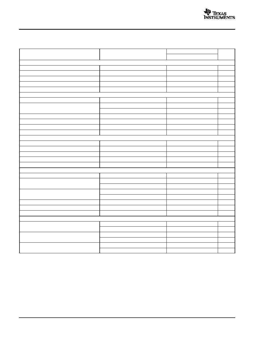
ORDERING INFORMATION
(1)
PRODUCT
MAXIMUM
INTEGRAL
LINEARITY
ERROR
(%FS)
MAXIMUM
GAIN
ERROR
(%)
PACKAGE-
LEAD
PACKAGE
DESIGNATOR
SPECIFIED
TEMPERATURE
RANGE
PACKAGE
MARKING
ORDERING
NUMBER
TRANSPORT MEDIA,
QUANTITY
ADS1206
�
0.012
�
0.7
VSSOP-8
DGK
-40
�
C to +85
�
C
TBD
ADS1206IDGKT
Tape and Reel, 250
ADS1206
�
0.012
�
0.7
VSSOP-8
DGK
-40
�
C to +85
�
C
TBD
ADS1206IDGKR
Tape and Reel, 2000
ADS1207
�
0.012
�
0.7
VSSOP-8
DGK
-40
�
C to +85
�
C
TBD
ADS1207IDGKT
Tape and Reel, 250
ADS1207
�
0.012
�
0.7
VSSOP-8
DGK
-40
�
C to +85
�
C
TBD
ADS1207IDGKR
Tape and Reel, 2000
(1) For the most current package and ordering information, refer to our web site at www.ti.com.
ABSOLUTE MAXIMUM RATINGS
over operating free-air temperature range unless otherwise noted(1)
ADS1204
UNIT
Supply Voltage, GND to VDD
-0.3 to 7
V
Analog Input Voltage with Respect to GND
GND - 0.3 to VDD + 0.3
V
Reference Input Voltage with Respect to GND
GND - 0.3 to VDD + 0.3
V
Digital Input Voltage with Respect to GND
GND - 0.3 to VDD + 0.3
V
Input Current to Any Pin Except Supply
-20 to 20
mA
Power Dissipation
See Dissipation Rating Table
Operating Virtual Junction Temperature Range, TJ
-40 to +150
�
C
Operating Free-Air Temperature Range, TA
-40 to +85
�
C
Storage Temperature Range, TSTG
-65 to +150
�
C
Lead Temperature (1.6mm or 1/16-inch from case for 10s)
+260
�
C
(1) Stresses beyond those listed under "absolute maximum ratings" may cause permanent damage to the device. These are stress ratings only, and
functional operation of the device at these or any other conditions beyond those indicated under "recommended operating conditions" is not
implied. Exposure to absolute-maximum-rated conditions for extended periods may affect device reliability.
RECOMMENDED OPERATING CONDITIONS
PARAMETER
MIN
NOM
MAX
UNIT
Supply Voltage, GND to VDD
Low-Voltage Levels
3.0
3.6
V
Supply Voltage, GND to VDD
5V Logic Levels
4.5
5
5.5
V
Reference Input Voltage
TBD
2.5
VDD
V
Analog Inputs
BUF = 0
0
VREF
V
Analog Inputs
BUF = 1
0.1
VDD - 0.2
V
External Clock
ADS1206
TBD
1
MHz
External Clock
ADS1207
TBD
4
MHz
Operating Junction Temperature Range, TJ
-40
105
�
C
(1) with reduced accuracy, minimum clock can go up to 500kHz.
DISSIPATION RATING TABLE
BOARD
PACKAGE
TA
25
�
C
POWER RATING
DERATING FACTOR
ABOVE TA = 25
�
C(1)
TA = 70
�
C
POWER RATING
TA = 85
�
C
POWER RATING
Low-K(2)
DGK
469.6mW
3.756mW/
�
C
300.5mW
244.2mW
High-K(3)
DGK
691.4mW
5.531mW/
�
C
442.5mW
359.5mW
(1) This is the inverse of the traditional junction-to-ambient thermal resistance (R
q
JA). Thermal resistances are not production tested and are for
informational purposes only.
(2) The JEDEC Low-K (1s) board design used to derive this data was a 3-inch x 3-inch, two-layer board with 2-ounce copper traces on top of the board.
(3) The JEDEC High-K (2s2p) board design used to derive this data was a 3-inch x 3-inch, multilayer board with 1-ounce internal power and ground
planes and 2-ounce copper traces on the top and bottom of the board.
PRODUCT PREVIEW

ADS1206
ADS1207
SBAS311 - MARCH 2004
www.ti.com
3
ELECTRICAL CHARACTERISTICS
Over recommended operating free-air temperature range at -40
�
C to +85
�
C, VDD = 5V or VDD = 3V, VREF = internal +2.5V, CLKIN = 1MHz, unless
otherwise noted.
ADS1206I, ADS1207I
PARAMETER
TEST CONDITIONS
MIN
TYP(1)
MAX
UNITS
DC Accuracy
INL
Integral linearity error(2)
BUF = 1
�
0.012
% FSR
INL
Integral linearity error(2)
BUF = 0
�
0.018
% FSR
DNL
Differential nonlinearity(3)
TBD
% FSR
VOS
Offset error
BUF = 0, VIN = 0V
�
7
�
35
mV
VOS
Offset error
BUF = 1, VIN = 0.1V
�
7
�
35
mV
TCVOS
Offset error drift
5
20
�
V/
�
C
GERR
Gain error(4)
Referenced to VREF
�
0.1
�
0.7
% FSR
TCGERR
Gain error drift
20
ppm/
�
C
Noise
TBD
�
Vrms
PSRR
Power-supply rejection ratio
4.5V < VDD < 5.5V
55
dB
PSRR
Power-supply rejection ratio
3.0V < VDD < 3.6V
65
dB
Analog Input
FSR
Full-scale range
BUF = 0
0
VREF
V
FSR
Full-scale range
BUF = 1
0.1
VDD - 0.2
V
Input capacitance
BUF = 0
3
pF
Input capacitance
BUF = 1
3
pF
Input current
BUF = 0
8
10
�
A
Input current
BUF = 1
5
100
nA
Differential input resistance
100
k
Differential input capacitance
1
pF
BW
Bandwidth
FS sinewave, -3dB, BUF = 0
TBD
MHz
BW
Bandwidth
FS sinewave, -3dB, BUF = 1
TBD
MHz
Output Signal
FOUT
Output frequency span
ADS1206I
0.1
0.9
CLKIN
FOUT
Output frequency span
ADS1207I
0.05
0.45
CLKIN
Voltage Reference Output
VOUT
Reference voltage output
2.3
2.5
2.7
V
Initial accuracy
�
8
%
dVOUT/dT
Output voltage temperature drift
�
50
ppm/
�
C
Output voltage noise
f = 0.1Hz to 10Hz, CL = 10
�
F
100
�
VPP
Output voltage noise
f =10Hz to 10kHz, CL = 10
�
F
TBD
�
Vrms
PSRR
Power-supply rejection ratio
VDD = 4.5V to 5.5V
-70
dB
PSRR
Power-supply rejection ratio
VDD = 3.0V to 3.6V
-60
dB
Reference output resistance
1
k
Turn-on settling time
to 0.1% at CL = 0
30
�
s
Voltage Reference Input
VREF
Reference voltage input
TBD
2.5
VDD
V
Reference input capacitance
5
pF
Reference input current
�
200
�
A
(1) All typical values are at TA = +25
�
C.
(2) Integral nonlinearity is defined as the maximum deviation of the line through the end points of the transfer curve for VIN = 0V to VREF or 0.1V
to VDD - 0.2V, expressed either as the number of LSBs or as a percent of measured input range.
(3) Ensured by design.
(4) Maximum values, including temperature drift, are ensured over the full specified temperature range.
(5) Applicable for 5.0V nominal supply: VDD (min) = 4.5V and VDD (max) = 5.5V.
(6) Applicable for 3.0V nominal supply: VDD (min) = 3.0V and VDD (max) = 3.6V.
PRODUCT PREVIEW
ADS1206
ADS1207
SBAS311 - MARCH 2004
www.ti.com
4
ELECTRICAL CHARACTERISTICS (continued)
Over recommended operating free-air temperature range at -40
�
C to +85
�
C, VDD = 5V or VDD = 3V, VREF = internal +2.5V, CLKIN = 1MHz, unless
otherwise noted.
PARAMETER
UNITS
ADS1206I, ADS1207I
TEST CONDITIONS
PARAMETER
UNITS
MAX
TYP(1)
MIN
TEST CONDITIONS
Digital Inputs(5)
Logic family
CMOS
VIH
High-level input voltage
0.7
�
VDD
VDD+0.3
V
VIL
Low-level input voltage
-0.3
0.3
�
VDD
V
IIN
Input current
VI = VDD or GND
�
1
�
A
CI
Input capacitance
5
pF
Digital Outputs(5)
Logic family
CMOS
VOH
High-level output voltage
VDD = 4.5V, IOH = -100
�
A
4.44
V
VOH
High-level output voltage
VDD = 4.5V, IOH = -2mA
2.5
V
VOL
Low-level output voltage
VDD = 4.5V, IOH = 2mA
0.5
V
IO
Output sink current
1.5V < VOL < VDD
10
mA
CO
Output capacitance
5
pF
CL
Load capacitance
30
pF
Digital Inputs(6)
Logic family
LVCMOS and LVTTL
VIH
High-level input Voltage
VDD = 3.6V
2
VDD+0.3
V
VIL
Low-level input voltage
VDD = 3.0V
-0.3
0.8
V
IIN
Input current
VI = VDD or GND
�
1
nA
CI
Input capacitance
5
pF
Digital Outputs(6)
Logic family
LVCMOS and LVTTL
VOH
High-level output voltage
VDD = 3V, IOH = -100
�
A
VDD-0.2
V
VOH
High-level output voltage
VDD = 3V, IOH = -2mA
2.4
V
VOL
Low-level output voltage
VDD = 3V, IOH = 100
�
A
0.2
V
VOL
Low-level output voltage
VDD = 3V, IOH = 2mA
0.4
V
IO
Output sink current
10
mA
CO
Output capacitance
5
pF
CL
Load capacitance
30
pF
Power Supply
VDD
Power-supply voltage
Low-voltage levels
3.0
3.6
V
VDD
Power-supply voltage
5V logic levels
4.5
5.5
V
IDD
Supply current
BUF = GND
0.9
1.25
mA
IDD
Supply current
BUF = VDD
1.1
1.5
mA
Power dissipation
VDD = 3.3V
3.63
4.95
mW
Power dissipation
VDD = 5V
5.5
7.5
mW
(1) All typical values are at TA = +25
�
C.
(2) Integral nonlinearity is defined as the maximum deviation of the line through the end points of the transfer curve for VIN = 0V to VREF or 0.1V
to VDD - 0.2V, expressed either as the number of LSBs or as a percent of measured input range.
(3) Ensured by design.
(4) Maximum values, including temperature drift, are ensured over the full specified temperature range.
(5) Applicable for 5.0V nominal supply: VDD (min) = 4.5V and VDD (max) = 5.5V.
(6) Applicable for 3.0V nominal supply: VDD (min) = 3.0V and VDD (max) = 3.6V.
PRODUCT PREVIEW

ADS1206
ADS1207
SBAS311 - MARCH 2004
www.ti.com
5
PIN ASSIGNMENTS
VSSOP PACKAGE
(TOP VIEW)
1
2
3
4
8
7
6
5
BUF
FOUT
V
DD
VIN
CLKOUT
CLKIN
GND
REFIN/OUT
Terminal Functions
TERMINAL
NAME
NO.
DESCRIPTION
CLKOUT
1
Clock output
CLKIN
2
Master clock input
GND
3
Ground
REFIN/OUT
4
Reference voltage input or output
VIN
5
Analog input
VDD
6
Power supply, +3.3V or +5V nominal
FOUT
7
Modulator output
BUF
8
Buffered mode select
PARAMETER MEASUREMENT INFORMATION
CLKIN
t
C1
t
W2
t
W1
t
D1
t
R1
t
F1
FOUT
Figure 1. Timing Diagram
TIMING REQUIREMENTS: 5.0V
over recommended operating free-air temperature range at -40
�
C to +85
�
C,, and VDD = 5V, unless otherwise noted.
PARAMETER
MIN
MAX
UNITS
tC1
Input clock period
ADS1206
1000
TBD
ns
tC1
Input clock period
ADS1207
250
TBD
ns
tW1
Input clock high time
(tC1/2) - 100
(tC1/2) + 100
ns
tD1
FOUT rising edge delay after input clock rising edge
TBD
TBD
ns
tW2
FOUT high time
tC1 - 20
tC1 + 20
ns
tR1
FOUT rise time
TBD
TBD
ns
tF1
FOUT fall time
TBD
TBD
ns
NOTE: Applicable for 5.0V nominal supply: VDD (min) = 4.5V and VDD (max) = 5.5V. All input signals are specified with tR = tF = 5ns (10% to 90%
of VDD) and timed from a voltage level of (VIL + VIH)/2. See timing diagram.
TIMING REQUIREMENTS: 3.3V
over recommended operating free-air temperature range at -40
�
C to +85
�
C,, and VDD = 3.3V, unless otherwise noted.
PARAMETER
MIN
MAX
UNITS
tC1
Input clock period
ADS1206
1000
TBD
ns
tC1
Input clock period
ADS1207
250
TBD
ns
tW1
Input clock high time
(tC1/2) - 100
(tC1/2) + 100
ns
tD1
FOUT rising edge delay after input clock rising edge
TBD
TBD
ns
tW2
FOUT high time
tC1 - 8
tC1 + 8
ns
tR1
FOUT rise time
TBD
TBD
ns
tF1
FOUT fall time
TBD
TBD
ns
NOTE: Applicable for 3.3V nominal supply: VDD (min) = 3.0V and VDD (max) = 3.6V. All input signals are specified with tR = tF = 5ns (10% to 90%
of VDD) and timed from a voltage level of (VIL + VIH)/2. See timing diagram.
PRODUCT PREVIEW

PACKAGING INFORMATION
Orderable Device
Status
(1)
Package
Type
Package
Drawing
Pins Package
Qty
Eco Plan
(2)
Lead/Ball Finish
MSL Peak Temp
(3)
ADS1206IDGKR
PREVIEW
MSOP
DGK
8
2500
None
Call TI
Call TI
ADS1206IDGKT
PREVIEW
MSOP
DGK
8
250
None
Call TI
Call TI
ADS1207IDGKR
PREVIEW
MSOP
DGK
8
None
Call TI
Call TI
ADS1207IDGKT
PREVIEW
MSOP
DGK
8
None
Call TI
Call TI
(1)
The marketing status values are defined as follows:
ACTIVE: Product device recommended for new designs.
LIFEBUY: TI has announced that the device will be discontinued, and a lifetime-buy period is in effect.
NRND: Not recommended for new designs. Device is in production to support existing customers, but TI does not recommend using this part in
a new design.
PREVIEW: Device has been announced but is not in production. Samples may or may not be available.
OBSOLETE: TI has discontinued the production of the device.
(2)
Eco Plan - May not be currently available - please check
http://www.ti.com/productcontent
for the latest availability information and additional
product content details.
None: Not yet available Lead (Pb-Free).
Pb-Free (RoHS): TI's terms "Lead-Free" or "Pb-Free" mean semiconductor products that are compatible with the current RoHS requirements
for all 6 substances, including the requirement that lead not exceed 0.1% by weight in homogeneous materials. Where designed to be soldered
at high temperatures, TI Pb-Free products are suitable for use in specified lead-free processes.
Green (RoHS & no Sb/Br): TI defines "Green" to mean "Pb-Free" and in addition, uses package materials that do not contain halogens,
including bromine (Br) or antimony (Sb) above 0.1% of total product weight.
(3)
MSL, Peak Temp. -- The Moisture Sensitivity Level rating according to the JEDECindustry standard classifications, and peak solder
temperature.
Important Information and Disclaimer:The information provided on this page represents TI's knowledge and belief as of the date that it is
provided. TI bases its knowledge and belief on information provided by third parties, and makes no representation or warranty as to the
accuracy of such information. Efforts are underway to better integrate information from third parties. TI has taken and continues to take
reasonable steps to provide representative and accurate information but may not have conducted destructive testing or chemical analysis on
incoming materials and chemicals. TI and TI suppliers consider certain information to be proprietary, and thus CAS numbers and other limited
information may not be available for release.
In no event shall TI's liability arising out of such information exceed the total purchase price of the TI part(s) at issue in this document sold by TI
to Customer on an annual basis.
PACKAGE OPTION ADDENDUM
www.ti.com
25-Feb-2005
Addendum-Page 1


IMPORTANT NOTICE
Texas Instruments Incorporated and its subsidiaries (TI) reserve the right to make corrections, modifications,
enhancements, improvements, and other changes to its products and services at any time and to discontinue
any product or service without notice. Customers should obtain the latest relevant information before placing
orders and should verify that such information is current and complete. All products are sold subject to TI's terms
and conditions of sale supplied at the time of order acknowledgment.
TI warrants performance of its hardware products to the specifications applicable at the time of sale in
accordance with TI's standard warranty. Testing and other quality control techniques are used to the extent TI
deems necessary to support this warranty. Except where mandated by government requirements, testing of all
parameters of each product is not necessarily performed.
TI assumes no liability for applications assistance or customer product design. Customers are responsible for
their products and applications using TI components. To minimize the risks associated with customer products
and applications, customers should provide adequate design and operating safeguards.
TI does not warrant or represent that any license, either express or implied, is granted under any TI patent right,
copyright, mask work right, or other TI intellectual property right relating to any combination, machine, or process
in which TI products or services are used. Information published by TI regarding third-party products or services
does not constitute a license from TI to use such products or services or a warranty or endorsement thereof.
Use of such information may require a license from a third party under the patents or other intellectual property
of the third party, or a license from TI under the patents or other intellectual property of TI.
Reproduction of information in TI data books or data sheets is permissible only if reproduction is without
alteration and is accompanied by all associated warranties, conditions, limitations, and notices. Reproduction
of this information with alteration is an unfair and deceptive business practice. TI is not responsible or liable for
such altered documentation.
Resale of TI products or services with statements different from or beyond the parameters stated by TI for that
product or service voids all express and any implied warranties for the associated TI product or service and
is an unfair and deceptive business practice. TI is not responsible or liable for any such statements.
Following are URLs where you can obtain information on other Texas Instruments products and application
solutions:
Products
Applications
Amplifiers
amplifier.ti.com
Audio
www.ti.com/audio
Data Converters
dataconverter.ti.com
Automotive
www.ti.com/automotive
DSP
dsp.ti.com
Broadband
www.ti.com/broadband
Interface
interface.ti.com
Digital Control
www.ti.com/digitalcontrol
Logic
logic.ti.com
Military
www.ti.com/military
Power Mgmt
power.ti.com
Optical Networking
www.ti.com/opticalnetwork
Microcontrollers
microcontroller.ti.com
Security
www.ti.com/security
Telephony
www.ti.com/telephony
Video & Imaging
www.ti.com/video
Wireless
www.ti.com/wireless
Mailing Address:
Texas Instruments
Post Office Box 655303 Dallas, Texas 75265
Copyright
2005, Texas Instruments Incorporated