 | –≠–ª–µ–∫—Ç—Ä–æ–Ω–Ω—ã–π –∫–æ–º–ø–æ–Ω–µ–Ω—Ç: ADS1222 | –°–∫–∞—á–∞—Ç—å:  PDF PDF  ZIP ZIP |
Document Outline
- FEATURES
- APPLICATIONS
- DESCRIPTION
- ORDERING INFORMATION
- ABSOLUTE MAXIMUM RATINGS
- ELECTRICAL CHARACTERISTICS
- PIN ASSIGNMENTS
- Terminal Functions
- TYPICAL CHARACTERISTICS
- OVERVIEW
- ANALOG INPUTS (AINPx, AINNx)
- Analog Input Measurement without the Input Buffer
- Analog Input Measurement with the Input Buffer
- TEMPERATURE SENSOR
- VOLTAGE REFERENCE INPUTS ( VREFP, VREFN)
- CLOCK INPUT (CLK)
- DATA READY/DATA OUTPUT (DRDY\/DOUT)
- SERIAL CLOCK INPUT (SCLK)
- FREQUENCY RESPONSE
- SETTLING TIME
- DATA FORMAT
- DATA RETRIEVAL
- SELF-CALIBRATION
- STANDBY MODE
- Standby Mode With Self-Calibration
- SINGLE CONVERSIONS
- APPLICATIONS INFORMATION
- GENERAL RECOMMENDATIONS
- MULTICHANNEL SYSTEMS
- SUMMARY OF SERIAL INTERFACE WAVEFORMS

SBAS314A - APRIL 2004 - REVISED SEPTEMBER 2004
24 Bit Analog to Digital Converter
with 2 Channel Differential Input Multiplexer
ADS1222
FEATURES
D
240SPS Data Rate with 4MHz Clock
D
20-Bit Effective Resolution
D
Input Multiplexer with Two Differential
Channels
D
Pin-Selectable, High-Impedance Input Buffer
D
±
5V Differential Input Range
D
0.0003% INL (typ), 0.0015% INL (max)
D
Self-Calibrating
D
Simple 2-Wire Serial Interface
D
On-Chip Temperature Sensor
D
Single Conversions with Standby Mode
D
Low Current Consumption: 300
µ
A
D
Analog Supply: 2.7V to 5.5V
APPLICATIONS
D
Hand-Held Instrumentation
D
Portable Medical Equipment
D
Industrial Process Control
D
Weigh Scales
DESCRIPTION
The ADS1222 is a 2-channel, 24-bit, delta-sigma ana-
log-to-digital (A/D) converter. It offers excellent perfor-
mance and low power in a TSSOP-14 package. The
ADS1222 is well-suited for demanding, high-resolution
measurements, especially in portable systems and oth-
er space-saving and power-constrained applications.
A delta-sigma modulator and digital filter form the basis
of the A/D converter. The analog modulator has a
±
5V
differential input range. An input multiplexer (mux) is
used to select between two separate differential input
channels. A buffer can be selected to increase the input
impedance of the measurement.
A simple, 2-wire serial interface provides all the
necessary control. Data retrieval, self-calibration, and
Standby mode are handled with a few simple
waveforms. When only single conversions are needed,
the ADS1222 can be quickly shut down (Standby mode)
while idle between measurements to dramatically
reduce the overall power consumption. Multiple
ADS1222s can be connected together to create a
synchronously sampling multichannel measurement
system. The ADS1222 is designed to easily connect to
microcontrollers, such as the MSP430.
The ADS1222 supports 2.7V to 5.5V supplies. Power
is typically less than 1mW in 3V operation and less than
1
µ
W during Standby mode.
Mux
Digital Filter
and
Serial Interface
Modulator
VREFP VREFN
Buffer
VDD
GND
MUX
AINP1
AINN1
AINP2
AINN2
CLK
DRDY/DOUT
SCLK
TEMPEN
BUFEN
www.ti.com
Copyright
2004, Texas Instruments Incorporated
Please be aware that an important notice concerning availability, standard warranty, and use in critical applications of Texas Instruments
semiconductor products and disclaimers thereto appears at the end of this data sheet.
All trademarks are the property of their respective owners.
PRODUCTION DATA information is current as of publication date. Products
conform to specifications per the terms of Texas Instruments standard warranty.
Production processing does not necessarily include testing of all parameters.
ADS1222
SBAS314A - APRIL 2004 - REVISED SEPTEMBER 2004
www.ti.com
2
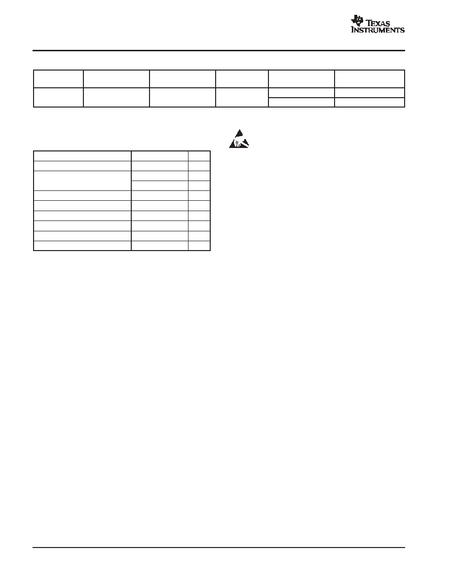
ORDERING INFORMATION
PRODUCT
PACKAGE-LEAD
PACKAGE
DESIGNATOR(1)
PACKAGE
MARKING
ORDERING NUMBER
TRANSPORT MEDIA,
QUANTITY
ADS1222
TSSOP-14
PW
ADS1222
ADS1222IPWT
Tape and Reel, 250
ADS1222
TSSOP-14
PW
ADS1222
ADS1222IPWR
Tape and Reel, 2000
(1) For the most current specification and package information, refer to our web site at www.ti.com.
ABSOLUTE MAXIMUM RATINGS
over operating free-air temperature range unless otherwise noted(1)
ADS1222
UNIT
VDD to GND
-0.3 to +6
V
Input current
100, momentary
mA
Input current
10, continuous
mA
Analog input voltage to GND
-0.3 to VDD + 0.3
V
Digital input voltage to GND
-0.3 to VDD + 0.3
V
Maximum Junction Temperature
+150
∞
C
Operating Temperature Range
-55 to +125
∞
C
Storage Temperature Range
-60 to +150
∞
C
Lead Temperature (soldering, 10s)
+300
∞
C
(1) Stresses above these ratings may cause permanent damage.
Exposure to absolute maximum conditions for extended periods
may degrade device reliability. These are stress ratings only, and
functional operation of the device at these or any other conditions
beyond those specified is not implied.
This integrated circuit can be damaged by ESD. Texas
Instruments recommends that all integrated circuits be
handled with appropriate precautions. Failure to observe
proper handling and installation procedures can cause damage.
ESD damage can range from subtle performance degradation to
complete device failure. Precision integrated circuits may be more
susceptible to damage because very small parametric changes could
cause the device not to meet its published specifications.
ADS1222
SBAS314A - APRIL 2004 - REVISED SEPTEMBER 2004
www.ti.com
3
ELECTRICAL CHARACTERISTICS
All specifications at TA = -40
∞
C to +85
∞
C, VDD = +5V, fCLK = 2MHz, and VREF = +2.5V, unless otherwise noted.
PARAMETER
TEST CONDITIONS
MIN
TYP
MAX
UNIT
Analog Input
Full-scale input voltage
AINP - AINN
±
2VREF
V
Absolute input voltage
Buffer off; AINP, AINN with respect to GND
GND - 0.1
VDD + 0.1
V
Absolute input voltage
Buffer on; AINP, AINN with respect to GND
GND + 0.05
VDD - 1.5
V
Differential input impedance
Buffer off; fCLK = 2MHz
2.7
M
Differential input impedance
Buffer on; fCLK = 2MHz
1.2
G
Common-mode input impedance
Buffer off; fCLK = 2MHz
5.4
M
System Performance
Resolution
No missing codes
24
Bits
Data rate
120 (fCLK/2MHz)
SPS(1)
Integral nonlinearity (INL)
Buffer off; Differential input signal, end point fit
0.0003
0.0015
% of FSR(2)
Integral nonlinearity (INL)
Buffer on; Differential input signal, end point fit
0.0006
% of FSR
Offset error
Buffer off
50
150
µ
V
Offset error
Buffer on
50
µ
V
Offset error drift
Buffer off
0.2
µ
V/
∞
C
Offset error drift
Buffer on
0.2
µ
V/
∞
C
Offset error match
Between channels
20
100
µ
V
Gain error
Buffer off
0.004
0.025
%
Gain error
Buffer on
0.008
%
Gain error drift
Buffer off
0.00003
% of FSR/
∞
C
Gain error drift
Buffer on
0.00006
% of FSR/
∞
C
Gain error match
Between channels
0.0005
%
Common-mode rejection
Buffer off; at DC
95
dB
Common-mode rejection
Buffer on; at DC
90
100
dB
Power-supply rejection
Buffer off; at DC, VDD = 2.7V to 5.5V
90
dB
Power-supply rejection
Buffer on; at DC, VDD = 2.7V to 5.5V
90
dB
Noise
0.8
ppm of FSR, rms
Temperature Sensor
Temperature sensor voltage
TA = 25
∞
C
106
mV
Temperature sensor coefficient
360
µ
V/
∞
C
Voltage Reference Input
Reference input voltage
VREF = VREFP - VREFN
0.5
2.5
VDD(3)
V
Negative reference input
Buffer off
GND - 0.1
VREFP - 0.5
V
Positive reference input
Buffer off
VREFN + 0.5
VDD + 0.1
V
Negative reference input
Buffer on
GND + 0.05
VREFP - 0.5
V
Positive reference input
Buffer on
VREFN + 0.5
VDD - 1.5
V
Voltage reference impedance
fCLK = 2MHz
500
k
(1) SPS = samples per second.
(2) FSR = full-scale range = 4VREF.
(3) It will not be possible to reach the digital output full-scale code when VREF > VDD/2.

ADS1222
SBAS314A - APRIL 2004 - REVISED SEPTEMBER 2004
www.ti.com
4
ELECTRICAL CHARACTERISTICS (continued)
All specifications at TA = -40
∞
C to +85
∞
C, VDD = +5V, fCLK = 2MHz, and VREF = +2.5V, unless otherwise noted.
PARAMETER
UNIT
MAX
TYP
MIN
TEST CONDITIONS
Digital Input/Output
VIH
0.8 VDD
VDD + 0.1
V
Logic
VIL
GND - 0.1
0.2 VDD
V
Logic
levels
VOH
IOH = 1mA
0.8 VDD
V
levels
VOL
IOL = 1mA
0.2 VDD
V
Input leakage
±
10
µ
A
CLK frequency (fCLK)
8
MHz
CLK duty cycle
30
70
%
Power Supply
VDD
2.7
5.5
V
Standby mode
< 1
µ
A
VDD = 5V, normal mode, buffer off
300
µ
A
VDD current
VDD = 5V, normal mode, buffer on
425
µ
A
VDD current
VDD = 3V, normal mode, buffer off
275
µ
A
VDD = 3V, normal mode, buffer on
395
µ
A
Total power dissipation
VDD = 5V, buffer off
1.5
2.25
mW
Total power dissipation
VDD = 3V, buffer off
0.8
mW
Temperature Range
Specified
-40
+85
∞
C
Operating
-55
+125
∞
C
Storage
-60
+150
∞
C
(1) SPS = samples per second.
(2) FSR = full-scale range = 4VREF.
(3) It will not be possible to reach the digital output full-scale code when VREF > VDD/2.

ADS1222
SBAS314A - APRIL 2004 - REVISED SEPTEMBER 2004
www.ti.com
5
PIN ASSIGNMENTS
PW PACKAGE
TSSOP-14
(TOP VIEW)
VDD
SCLK
CLK
DRDY/DOUT
MUX
TEMPEN
BUFEN
VREFP
VREFN
GND
AINN1
AINP1
AINN2
AINP2
1
2
3
4
5
6
7
14
13
12
11
10
9
8
ADS1222
Terminal Functions
TERMINAL
NAME
NO.
I/O
DESCRIPTION
VDD
1
Analog/Digital
Analog and digital power supply
SCLK
2
Digital input
Serial clock input
CLK
3
Digital input
System clock input
DRDY/DOUT
4
Digital Output
Dual-purpose output:
Data ready: indicates valid data by going low.
Data output: outputs data, MSB first, on the rising edge of SCLK.
MUX
5
Digital input
Selects analog input of mux
TEMPEN
6
Digital input
Selects temperature sensor input from mux
BUFEN
7
Digital input
Enables input buffer
AINP2
8
Analog input
Analog channel 2 positive input
AINN2
9
Analog input
Analog channel 2 negative input
AINP1
10
Analog input
Analog channel 1 positive input
AINN1
11
Analog input
Analog channel 1 negative input
GND
12
Analog/Digital
Analog and digital ground
VREFN
13
Analog input
Negative reference input
VREFP
14
Analog input
Positive reference input