SBAS322 - DECEMBER 2004
16 Bit, 1.25MSPS
Analog to Digital Converter
ADS1601
FEATURES
D
High Speed:
Data Rate: 1.25MSPS
Bandwidth: 615kHz
D
Outstanding Performance:
SNR: 92dB at f
IN
= 100kHz, -1dBFS
THD: -103dB at f
IN
= 100kHz, -6dBFS
SFDR: 105dB at f
IN
= 100kHz, -6dBFS
D
Ease-of-Use:
High-Speed 3-Wire Serial Interface
Directly Connects to TMS320 DSPs
On-Chip Digital Filter Simplifies Anti-Alias
Requirements
Simple Pin-Driven Control--No On-Chip
Registers to Program
Selectable On-Chip Voltage Reference
Simultaneous Sampling with Multiple
ADS1601s
D
Low Power:
330mW at 1.25MSPS
145mW at 625kSPS
Power-Down Mode
APPLICATIONS
D
Sonar
D
Vibration Analysis
D
Data Acquisition
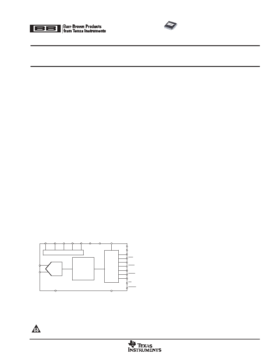
FSO
Reference and Bias Circuits
Serial
Interface
Linear Phase
FIR Digital Filter
Modulator
VREFP VREFN
RBIAS
VMID
VCAP
AVDD
DVDD
IOVDD
DGND
AGND
AINP
AINN
FSO
SCLK
DOUT
SCLK
SYNC
CLK
DOUT
OTR
PD
REFEN
ADS1601
DESCRIPTION
The ADS1601 is a high-speed, high-precision,
delta-sigma analog-to-digital converter (ADC)
manufactured on an advanced CMOS process. The
ADS1601 oversampling topology reduces clock jitter
sensitivity during the sampling of high-frequency, large
amplitude signals by a factor of four over that achieved by
Nyquist-rate ADCs. Consequently, signal-to-noise ratio
(SNR) is particularly improved. Total harmonic distortion
(THD) is -103dB, and the spurious-free dynamic range
(SFDR) is 105dB.
Optimized for power and performance, the ADS1601
dissipates only 330mW while providing a full-scale
differential input range of
±
3V. Having such a wide input
range makes out-of-range signals unlikely. The OTR pin
indicates if an analog input out-of-range condition does
occur. The differential input signal is measured against the
differential reference, which can be generated internally or
supplied externally on the ADS1601.
The ADS1601 uses an inherently stable advanced
modulator with an on-chip decimation filter. The filter stop
band extends to 19.3MHz, which greatly simplifies the
anti-aliasing circuitry. The modulator samples the input
signal up to 20MSPS, depending on f
CLK
, while the 16x
decimation filter uses a series of four half-band FIR filter
stages to provide 75dB of stop band attenuation and
0.001dB of passband ripple.
Output data is provided over a simple 3-wire serial
interface at rates up to 1.25MSPS, with a -3dB bandwidth
of 615kHz. The output data or its complementary format
directly connects to DSPs such as TI's TMS320 family,
FPGAs, or ASICs. A dedicated synchronization pin
enables simultaneous sampling with multiple ADS1601s
in multi-channel systems. Power dissipation is set by an
external resistor that allows a reduction in dissipation
when operating at slower speeds. All of the ADS1601
features are controlled by dedicated I/O pins, which
simplify operation by eliminating the need for on-chip
registers.
The high performing, easy-to-use ADS1601 is especially
suitable for demanding measurement applications in
sonar, vibration analysis, and data acquisition. The
ADS1601 is offered in a small, 7mm x 7mm TQFP-48
package and is specified from -40
∞
C to +85
∞
C.
All trademarks are the property of their respective owners.
PRODUCTION DATA information is current as of publication date. Products
conform to specifications per the terms of Texas Instruments standard warranty.
Production processing does not necessarily include testing of all parameters.
www.ti.com
Copyright
2004, Texas Instruments Incorporated
Please be aware that an important notice concerning availability, standard warranty, and use in critical applications of Texas Instruments
semiconductor products and disclaimers thereto appears at the end of this data sheet.
ADS1601
SBAS322 - DECEMBER 2004
www.ti.com
2
PACKAGE/ORDERING INFORMATION
For the most current package and ordering information see
the Package Option Addendum located at the end of this
datasheet.
ABSOLUTE MAXIMUM RATINGS
over operating free-air temperature range unless otherwise noted(1)
ADS1601
UNIT
AVDD to AGND
-0.3 to +6
V
DVDD to DGND
-0.3 to +3.6
V
IOVDD to DGND
-0.3 to +6
V
AGND to DGND
-0.3 to +0.3
V
Input Current
100mA, Momentary
Input Current
10mA, Continuous
Analog I/O to AGND
-0.3 to AVDD + 0.3
V
Digital I/O to DGND
-0.3 to IOVDD + 0.3
V
Maximum Junction Temperature
+150
∞
C
Operating Temperature Range
-40 to +105
∞
C
Storage Temperature Range
-60 to +150
∞
C
Lead Temperature (soldering, 10s)
+260
∞
C
(1) Stresses above these ratings may cause permanent damage.
Exposure to absolute maximum conditions for extended periods
may degrade device reliability. These are stress ratings only, and
functional operation of the device at these or any other conditions
beyond those specified is not implied.
This integrated circuit can be damaged by ESD. Texas
Instruments recommends that all integrated circuits be
handled with appropriate precautions. Failure to observe
proper handling and installation procedures can cause damage.
ADS1601 passes standard 200V machine model and 1.5K CDM
testing. ADS1601 passes 1kV human body model testing (TI Standard
is 2kV).
ESD damage can range from subtle performance degradation to
complete device failure. Precision integrated circuits may be more
susceptible to damage because very small parametric changes could
cause the device not to meet its published specifications.
ADS1601
SBAS322 - DECEMBER 2004
www.ti.com
3
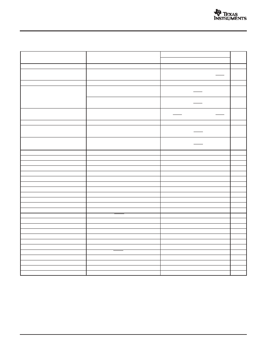
ELECTRICAL CHARACTERISTICS
All specifications at TA = -40
∞
C to +85
∞
C, AVDD = 5V, DVDD = IOVDD = 3V, fCLK = 20MHz, VREF = +3V, VCM = +2.7V, and RBIAS = 60k
,
unless otherwise noted.
ADS1601
PARAMETER
TEST CONDITIONS
MIN
TYP
MAX
UNIT
Analog Input
Differential input voltage (V
IN
)
(AINP - AINN)
0dBFS
±
V
REF
V
Common-mode input voltage (V
CM
)
(AINP + AINN) / 2
2.7
V
Differential input voltage (V
IN
)
(AINP or AINN with respect to AGND)
0dBFS
-0.1
3.5
V
Dynamic Specifications
Data Rate
1.25
f
CLK
20MHz
MSPS
f
IN
= 10kHz, -1dBFS
92
dB
f
IN
= 10kHz, -3dBFS
87
90
dB
f
IN
= 10kHz, -6dBFS
84
87
dB
f
IN
= 100kHz, -1dBFS
92
dB
Signal-to-noise ratio (SNR)
f
IN
= 100kHz, -3dBFS
87
90
dB
Signal-to-noise ratio (SNR)
f
IN
= 100kHz, -6dBFS
84
87
dB
f
IN
= 500kHz, -1dBFS
91
dB
f
IN
= 500kHz, -3dBFS
89
dB
f
IN
= 500kHz, -6dBFS
87
dB
f
IN
= 10kHz, -1dBFS
-91
dB
f
IN
= 10kHz, -3dBFS
-100
-90
dB
f
IN
= 10kHz, -6dBFS
-104
-97
dB
f
IN
= 100kHz, -1dBFS
-88
dB
Total harmonic distortion (THD)
f
IN
= 100kHz, -3dBFS
-96
-90
dB
Total harmonic distortion (THD)
f
IN
= 100kHz, -6dBFS
-103
-96
dB
f
IN
= 500kHz, -1dBFS
-115
dB
f
IN
= 500kHz, -3dBFS
-112
dB
f
IN
= 500kHz, -6dBFS
-110
dB
f
IN
= 10kHz, -1dBFS
88
dB
f
IN
= 10kHz, -3dBFS
85
89
dB
f
IN
= 10kHz, -6dBFS
84
87
dB
f
IN
= 100kHz, -1dBFS
87
dB
Signal-to-noise + distortion (SINAD)
f
IN
= 100kHz, -3dBFS
85
88
dB
Signal-to-noise + distortion (SINAD)
f
IN
= 100kHz, -6dBFS
84
86
dB
f
IN
= 500kHz, -1dBFS
91
dB
f
IN
= 500kHz, -3dBFS
89
dB
f
IN
= 500kHz, -6dBFS
87
dB
f
IN
= 10kHz, -1dBFS
92
dB
f
IN
= 10kHz, -3dBFS
91
100
dB
f
IN
= 10kHz, -6dBFS
98
109
dB
f
IN
= 100kHz, -1dBFS
88
dB
Spurious-free dynamic range (SFDR)
f
IN
= 100kHz, -3dBFS
90
97
dB
Spurious-free dynamic range (SFDR)
f
IN
= 100kHz, -6dBFS
97
105
dB
f
IN
= 500kHz, -1dBFS
120
dB
f
IN
= 500kHz, -3dBFS
118
dB
f
IN
= 500kHz, -6dBFS
115
dB
Intermodulation distortion (IMD)
f
1
= 499kHz, -6dBFS
94
dB
Intermodulation distortion (IMD)
f
2
= 501kHz, -6dBFS
94
dB
Aperture delay
4
ns
ADS1601
SBAS322 - DECEMBER 2004
www.ti.com
4
ELECTRICAL CHARACTERISTICS (continued)
All specifications at TA = -40
∞
C to +85
∞
C, AVDD = 5V, DVDD = IOVDD = 3V, fCLK = 20MHz, VREF = +3V, VCM = +2.7V, and RBIAS = 60k
,
unless otherwise noted.
ADS1601
PARAMETER
UNIT
MAX
TYP
MIN
TEST CONDITIONS
Digital Filter Characteristics
Passband
0
550
f
CLK
20MHz
kHz
Passband ripple
±
0.001
dB
Passband transition
-0.1dB attenuation
575
f
CLK
20MHz
kHz
Passband transition
-3.0dB attentuation
615
f
CLK
20MHz
kHz
Stop band
0.7
f
CLK
20MHz
19.3
f
CLK
20MHz
MHz
Stop band attenuation
75
dB
Group delay
20.8
20MHZ
f
CLK
µ
s
Settling time
Complete settling
40.8
20MHZ
f
CLK
µ
s
Static Specifications
Resolution
16
Bits
No missing codes
16
Bits
Input-referred noise
0.5
0.75
LSB, rms
Integral nonlinearity
-0.5dBFS signal
0.75
LSB
Differential nonlinearity
0.25
LSB
Offset error
-0.05
%FSR
Offset error drift
0.5
ppmFSR/
∞
C
Gain error
0.25
%
Gain error drift
Excluding reference drift
10
ppm/
∞
C
Common-mode rejection
At DC
75
dB
Power-supply rejection
At DC
65
dB
Internal Voltage Reference
REFEN = low
V
REF
= (VREFP - VREFN)
2.75
3
3.25
V
VREFP
3.5
3.8
4.1
V
VREFN
0.5
0.8
1.1
V
VMID
2.3
2.4
2.6
V
V
REF
drift
50
ppm/
∞
C
Startup time
15
ms
External Voltage Reference
REFEN = High
V
REF
= (VREFP - VREFN)
2.0
3
3.25
V
VREFP
3.5
4
4.25
V
VREFN
0.5
1
1.5
V
VMID
2.3
2.5
2.6
V

ADS1601
SBAS322 - DECEMBER 2004
www.ti.com
5
ELECTRICAL CHARACTERISTICS (continued)
All specifications at TA = -40
∞
C to +85
∞
C, AVDD = 5V, DVDD = IOVDD = 3V, fCLK = 20MHz, VREF = +3V, VCM = +2.7V, and RBIAS = 60k
,
unless otherwise noted.
ADS1601
PARAMETER
UNIT
MAX
TYP
MIN
TEST CONDITIONS
Clock Input
Frequency (f
CLK
)
20
MHz
Duty Cycle
f
CLK
= 20MHz
45
55
%
Digital Input/Output
V
IH
0.7 IOVDD
IOVDD
V
V
IL
DGND
0.3 IOVDD
V
V
OH
I
OH
= 50
µ
A
IOVDD - 0.5
V
V
OL
I
OL
= 50
µ
A
DGND + 0.5
V
Input leakage
DGND < V
DIGIN
< IOVDD
±
10
µ
A
Power-Supply Requirements
AVDD
4.75
5.25
V
DVDD
2.7
3.3
V
IOVDD
I
OH
= 50
µ
A
2.7
5.25
V
AVDD current (I
AVDD
)
REFEN = low
65
77
mA
AVDD current (I
AVDD
)
REFEN = high
55
65
mA
DVDD current (I
DVDD
)
IOVDD = 3V
15
18
mA
IOVDD current (I
IOVDD
)
IOVDD = 3V
3
8
mA
Power dissipation
AVDD = 5V, DVDD = 3V,
IOVDD = 3V, REFEN = high
330
380
mW
Power dissipation
PD = low, CLK disabled
10
mW
Temperature Range
Specified
-40
+85
∞
C
Operating
-40
+105
∞
C
Storage
-60
+150
∞
C