 | –≠–ª–µ–∫—Ç—Ä–æ–Ω–Ω—ã–π –∫–æ–º–ø–æ–Ω–µ–Ω—Ç: ADS5521 | –°–∫–∞—á–∞—Ç—å:  PDF PDF  ZIP ZIP |
SBAS308A - MAY 2004 - REVISED MARCH 2005
14 Bit, 80MSPS
Analog to Digital Converter
ADS5542
FEATURES
D
14-Bit Resolution
D
80MSPS Sample Rate
D
High SNR: 72.9dBFS at 100 MHz f
IN
D
High SFDR: 88dBc at 100 MHz f
IN
D
2.3V
PP
Differential Input Voltage
D
Internal Voltage Reference
D
3.3V Single-Supply Voltage
D
Analog Power Dissipation: 545mW
- Output Buffer Power: 129mW
D
TQFP-64 PowerPAD
E
Package
D
Recommended Op Amps:
THS3202, THS3201, THS4503,
OPA695, OPA847
D
Pin-Compatible with:
- ADS5500 (14-Bit, 125MSPS)
- ADS5541 (14-Bit, 105MSPS)
- ADS5520 (12-Bit, 125MSPS)
- ADS5521 (12-Bit, 105MSPS)
- ADS5522 (12-Bit, 80MSPS)
APPLICATIONS
D
Wireless Communication
- Communication Receivers
- Base Station Infrastructure
D
Test and Measurement Instrumentation
D
Single and Multichannel Digital Receivers
D
Communication Instrumentation
- Radar, Infrared
D
Video and Imaging
D
Medical Equipment
D
Military Equipment
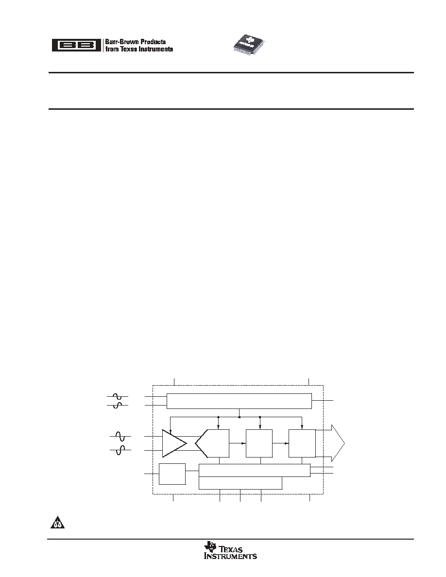
DESCRIPTION
The ADS5542 is a high-performance, 14-bit, 80MSPS analog-to-digital converter (ADC). To provide a complete converter
solution, it includes a high-bandwidth linear sample-and-hold stage (S&H) and internal reference. Designed for
applications demanding the highest speed and highest dynamic performance in very little space, the ADS5542 has
excellent analog power dissipation of 545mW and output buffer power dissipation of 129mW from a 3.3V single-supply
voltage. This allows an even higher system integration density. The provided internal reference simplifies system design
requirements. Parallel CMOS compatible output ensures seamless interfacing with common logic.
The ADS5542 is available in a 64-pin TQFP PowerPAD package and is pin-compatible with the ADS5500, ADS5541,
ADS5520, ADS5521, and ADS5522. This device is specified over the full temperature range of -40
∞
C to +85
∞
C.
14-Bit
Pipeline
ADC Core
S&H
CLK+
CLK
-
CLKOUT
V
IN
+
V
IN
-
Digital
Error
Correction
Timing Circuitry
Internal
Reference
Control Logic
Serial Programming Register
Output
Control
AV
DD
D0
.
.
.
D13
CM
OVR
DFS
ADS5542
A
GND
DR
GND
SEN
SDATA
SCLK
DRV
DD
PRODUCTION DATA information is current as of publication date. Products
conform to specifications per the terms of Texas Instruments standard warranty.
Production processing does not necessarily include testing of all parameters.
PowerPad is a trademark of Texas Instruments. All other trademarks are the property of their respective owners.
www.ti.com
Copyright
2004-2005, Texas Instruments Incorporated
Please be aware that an important notice concerning availability, standard warranty, and use in critical applications of Texas Instruments
semiconductor products and disclaimers thereto appears at the end of this data sheet.
ADS5542
SBAS308A - MAY 2004 - REVISED MARCH 2005
www.ti.com
2
PACKAGE/ORDERING INFORMATION
(1)
PRODUCT
PACKAGE-LEAD
PACKAGE
DESIGNATOR
SPECIFIED
TEMPERATURE
RANGE
PACKAGE
MARKING
ORDERING
NUMBER
TRANSPORT
MEDIA, QUANTITY
ADS5542
HTQFP-64
(2)
PAP
-40
∞
C to +85
∞
C
ADS5542I
ADS5542IPAP
Tray, 160
ADS5542
HTQFP-64
(2)
PowerPAD
PAP
-40
∞
C to +85
∞
C
ADS5542I
ADS5542IPAPR
Tape and Reel, 1000
(1) For the most current package and ordering information, see the Package Option Addendum at the end of this data sheet, or see the TI website
at www.ti.com.
(2) Thermal pad size: 3.5mm x 3.5mm (min), 4mm x 4mm (max).
JA
= 21.47
∞
C/W and
JC
= 2.99
∞
C/W, when used with 2oz. copper trace and pad
soldered directly to a JEDEC standard 4 layer 3in x 3in PCB.
This integrated circuit can be damaged by ESD. Texas Instruments recommends that all integrated circuits be handled with appropriate
precautions. Failure to observe proper handling and installation procedures can cause damage.
ESD damage can range from subtle performance degradation to complete device failure. Precision integrated circuits may be more susceptible to
damage because very small parametric changes could cause the device not to meet its published specifications.
ABSOLUTE MAXIMUM RATINGS
over operating free-air temperature range unless otherwise noted(1)
ADS5542
UNIT
Supply
Voltage
AV
DD
to A
GND
,
DRV
DD
to DR
GND
-0.3 to +3.7
V
Voltage
A
GND
to DR
GND
±
0.1
V
Analog input to A
GND
(2)
-0.3 to +3.6
V
Logic input to DR
GND
-0.3 to DRV
DD
V
Digital data output to DR
GND
-0.3 to DRV
DD
V
Operating temperature range
-40 to +85
∞
C
Junction temperature
+105
∞
C
Storage temperature range
-65 to +150
∞
C
(1) Stresses above these ratings may cause permanent damage.
Exposure to absolute maximum conditions for extended periods
may degrade device reliability. These are stress ratings only, and
functional operation of the device at these or any other conditions
beyond those specified is not implied.
(2) For more detail, refer to Input Voltage Overstress in the
Application Information section.
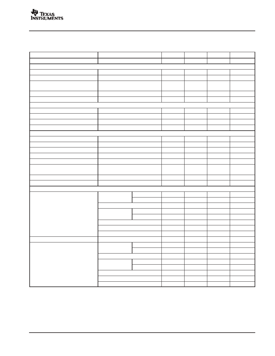
RECOMMENDED OPERATING CONDITIONS
PARAMETER
MIN
TYP
MAX
UNIT
Supplies
Analog supply voltage, AV
DD
3.0
3.3
3.6
V
Output driver supply voltage, DRV
DD
3.0
3.3
3.6
V
Analog Input
Differential input range
2.3
V
PP
Input common-mode voltage, V
CM
(1)
1.47
1.57
1.67
V
Digital Output
Maximum output load
10
pF
Clock Input
ADCLK input sample rate (sine
wave) 1/t
C
10
80
MSPS
Clock amplitude, sine wave,
differential(2)
1
3
V
PP
Clock duty cycle(3)
50
%
Open free-air temperature range
-40
+85
∞
C
(1) Input common-mode should be connected to CM.
(2) See Figure 46 for more information.
(3) See Figure 45 for more information.
ADS5542
SBAS308A - MAY 2004 - REVISED MARCH 2005
www.ti.com
3
ELECTRICAL CHARACTERISTICS
Typical values at T
A
= +25
∞
C, full temperature range is T
MIN
= -40
∞
C to T
MAX
= +85
∞
C, AV
DD
= DRV
DD
= 3.3V, sampling rate = 80MSPS,
50% clock duty cycle, 3VPP differential clock, and -1dBFS differential input, unless otherwise noted.
PARAMETER
CONDITIONS
MIN
TYP
MAX
UNIT
Resolution
14
Bits
Analog Inputs
Differential input range
2.3
V
PP
Differential input capacitance
See Figure 37
4
pF
Analog input common-mode current (per
input)
200
µ
A
Analog input bandwidth
Source impedance = 50
750
MHz
Voltage overload recovery time
4
Clock Cycles
Internal Reference Voltages
Reference bottom voltage, V
REFM
1.0
V
Reference top voltage, V
REFP
2.15
V
Reference error
-4
±
0.6
+4
%
Common-mode voltage output, V
CM
1.575
V
Dynamic DC Characteristics and Accuracy
No missing codes
Tested
Differential nonlinearity error, DNL
f
IN
= 10MHz
-0.9
±
0.5
1.1
LSB
Integral nonlinearity error, INL
f
IN
= 10MHz
-5.0
±
2.0
+5.0
LSB
Offset error
±
1.5
mV
Offset temperature coefficient
0.02
mV/
∞
C
DC power supply rejection ratio, DC PSRR
offset error/
AV
DD
from
AV
DD
= 3.0V to AV
DD
= 3.6V
0.25
mV/V
Gain error
±
0.3
%FS
Gain temperature coefficient
-0.02
%
/∞
C
Dynamic AC Characteristics
f
IN
= 10MHz
+25
∞
C to +85
∞
C
72.7
74.3
dBFS
f
IN
= 10MHz
Full temp range
71.5
74.0
dBFS
f
IN
= 55MHz
73.7
dBFS
Signal-to-noise ratio, SNR
f
IN
= 70MHz
+25
∞
C to +85
∞
C
71.5
73.5
dBFS
Signal-to-noise ratio, SNR
f
IN
= 70MHz
Full temp range
70.0
73.0
dBFS
f
IN
= 100MHz
72.9
dBFS
f
IN
= 150MHz
71.9
dBFS
f
IN
= 220MHz
70.7
dBFS
RMS idle channel noise
Input tied to common-mode
1.1
LSB
f
IN
= 10MHz
Room temp
80.0
92.0
dBc
f
IN
= 10MHz
Full temp range
78.0
90.0
dBc
f
IN
= 55MHz
88.0
dBc
Spurious-free dynamic range, SFDR
f
IN
= 70MHz
Room temp
80.0
87.0
dBc
Spurious-free dynamic range, SFDR
f
IN
= 70MHz
Full temp range
78.0
86.0
dBc
f
IN
= 100MHz
88.0
dBc
f
IN
= 150MHz
85.0
dBc
f
IN
= 220MHz
77.0
dBc

ADS5542
SBAS308A - MAY 2004 - REVISED MARCH 2005
www.ti.com
4
ELECTRICAL CHARACTERISTICS (continued)
Typical values at T
A
= +25
∞
C, full temperature range is T
MIN
= -40
∞
C to T
MAX
= +85
∞
C, AV
DD
= DRV
DD
= 3.3V, sampling rate = 80MSPS,
50% clock duty cycle, 3VPP differential clock, and -1dBFS differential input, unless otherwise noted.
PARAMETER
UNIT
MAX
TYP
MIN
CONDITIONS
f
IN
= 10MHz
Room temp
80.0
92.0
dBc
f
IN
= 10MHz
Full temp range
78.0
90.0
dBc
f
IN
= 55MHz
88.0
dBc
Second-harmonic, HD2
f
IN
= 70MHz
Room temp
80.0
87.0
dBc
Second-harmonic, HD2
f
IN
= 70MHz
Full temp range
78.0
86.0
dBc
f
IN
= 100MHz
88.0
dBc
f
IN
= 150MHz
85.0
dBc
f
IN
= 220MHz
77.0
dBc
f
IN
= 10MHz
Room temp
80.0
89.0
dBc
f
IN
= 10MHz
Full temp range
78.0
88.0
dBc
f
IN
= 55MHz
79.0
dBc
Third-harmonic, HD3
f
IN
= 70MHz
Room temp
80.0
85.0
dBc
Third-harmonic, HD3
f
IN
= 70MHz
Full temp range
78.0
83.0
dBc
f
IN
= 100MHz
83.0
dBc
f
IN
= 150MHz
80.0
dBc
f
IN
= 220MHz
76.0
dBc
Worst-harmonic/spur
f
IN
= 10MHz
Room temp
88.0
dBc
Worst-harmonic/spur
(other than HD2 and HD3)
f
IN
= 70MHz
Room temp
87.0
dBc
f
IN
= 10MHz
+25
∞
C to +85
∞
C
72.2
73.8
dBFS
f
IN
= 10MHz
Full temp range
71.0
73.5
dBFS
f
IN
= 55MHz
73.2
dBFS
Signal-to-noise + distortion, SINAD
f
IN
= 70MHz
+25
∞
C to +85
∞
C
71.0
73.2
dBFS
Signal-to-noise + distortion, SINAD
f
IN
= 70MHz
Full temp range
69.5
72.5
dBFS
f
IN
= 100MHz
72.5
dBFS
f
IN
= 150MHz
71.8
dBFS
f
IN
= 220MHz
69.8
dBFS
f
IN
= 10MHz
Room temp
78.0
90.0
dBc
f
IN
= 10MHz
Full temp range
76.0
88.0
dBc
f
IN
= 55MHz
83.4
dBc
Total harmonic distortion, THD
f
IN
= 70MHz
Room temp
78.0
86.0
dBc
Total harmonic distortion, THD
f
IN
= 70MHz
Full temp range
76.0
84.0
dBc
f
IN
= 100MHz
83.4
dBc
f
IN
= 150MHz
81.2
dBc
f
IN
= 220MHz
75.8
dBc
Effective number of bits, ENOB
f
IN
= 70MHz
11.9
Bits
f = 10.1MHz, 15.1MHz
(-7dBFS each tone)
93.8
dBFS
Two-tone intermodulation distortion, IMD
f = 50.1MHz, 55.1MHz
(-7dBFS each tone)
92.4
dBFS
f = 148.1MHz, 153.1MHz
(-7dBFS each tone)
92.6
dBFS
ADS5542
SBAS308A - MAY 2004 - REVISED MARCH 2005
www.ti.com
5
ELECTRICAL CHARACTERISTICS (continued)
Typical values at T
A
= +25
∞
C, full temperature range is T
MIN
= -40
∞
C to T
MAX
= +85
∞
C, AV
DD
= DRV
DD
= 3.3V, sampling rate = 80MSPS,
50% clock duty cycle, 3VPP differential clock, and -1dBFS differential input, unless otherwise noted.
PARAMETER
UNIT
MAX
TYP
MIN
CONDITIONS
Power Supply
Total supply current, I
CC
f
IN
= 70MHz
204
230
mA
Analog supply current, I
AVDD
f
IN
= 70MHz
165
180
mA
Output buffer supply current, I
DRVDD
f
IN
= 70MHz
39
50
mA
Analog only
545
594
mW
Power dissipation
Output buffer power with 10pF load on
digital output to ground
129
165
mW
Standby power
With clocks running
180
250
mW
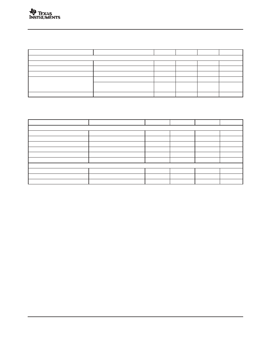
DIGITAL CHARACTERISTICS
Valid over full temperature range of T
MIN
= -40
∞
C to T
MAX
= +85
∞
C, AV
DD
= DRV
DD
= 3.3V, unless otherwise noted.
PARAMETER
CONDITIONS
MIN
TYP
MAX
UNIT
Digital Inputs
High-level input voltage, V
IH
2.4
V
Low-level input voltage, V
IL
0.8
V
High-level input current, I
IH
10
µ
A
Low-level input current, I
IL
10
µ
A
Input current for RESET
-20
µ
A
Input capacitance
4
pF
Digital Outputs
Low-level output voltage, V
OL
C
LOAD
= 10pF
0.3
0.4
V
High-level output voltage, V
OH
C
LOAD
= 10pF
2.4
3.0
V
Output capacitance
3
pF