 | –≠–ª–µ–∫—Ç—Ä–æ–Ω–Ω—ã–π –∫–æ–º–ø–æ–Ω–µ–Ω—Ç: ADS7817B | –°–∫–∞—á–∞—Ç—å:  PDF PDF  ZIP ZIP |
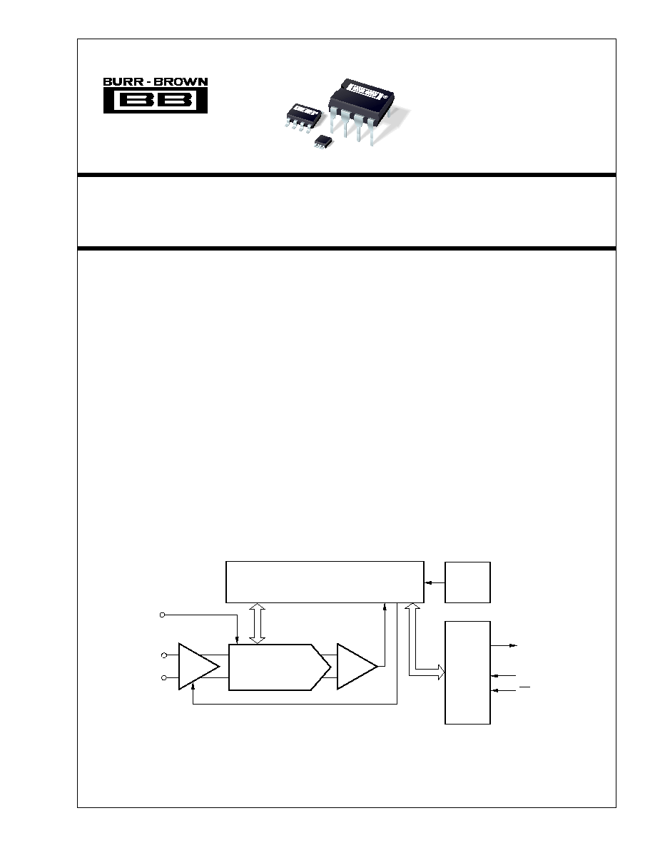
ADS7817
DESCRIPTION
The ADS7817 is a 12-bit, 200kHz sampling analog-
to-digital converter (A/D) that features a high imped-
ance fully differential analog input. The reference
voltage can be varied from 100mV to 2.5V, with a
corresponding input-referred resolution between 49
µ
V
and 1.22mV.
The differential input, low power, automatic power
down, and small size make the ADS7817 ideal for
direct connection to transducers in battery operated
systems, remote data acquisition, or multi-channel
applications. The ADS7817 is available in a plastic
mini-DIP-8, an SOIC-8, or an MSOP-8 package.
12-Bit Differential Input Micro Power Sampling
ANALOG-TO-DIGITAL CONVERTER
Æ
©
1997 Burr-Brown Corporation
PDS-1369B
Printed in U.S.A., May, 2000
FEATURES
q
BIPOLAR INPUT RANGE
q
TRUE DIFFERENTIAL INPUT
q
200kHz SAMPLING RATE
q
MICRO POWER: 2.3mW at 200kHz
q
POWER DOWN: 3
µ
A Max
q
AVAILABLE IN MSOP-8 PACKAGE
q
SERIAL INTERFACE
q
AC COMMON-MODE REJECTION
SAR
Control
Serial
Interface
D
OUT
Comparator
S/H Amp
CS/SHDN
DCLOCK
+In
V
REF
≠In
CDAC
OPA658
ADS7817
ADS7817
APPLICATIONS
q
TRANSDUCER INTERFACE
q
BATTERY OPERATED SYSTEMS
q
REMOTE DATA ACQUISITION
q
ISOLATED DATA ACQUISITION
q
AC MOTOR CONTROL
International Airport Industrial Park ∑ Mailing Address: PO Box 11400, Tucson, AZ 85734 ∑ Street Address: 6730 S. Tucson Blvd., Tucson, AZ 85706 ∑ Tel: (520) 746-1111
Twx: 910-952-1111 ∑ Internet: http://www.burr-brown.com/ ∑ Cable: BBRCORP ∑ Telex: 066-6491 ∑ FAX: (520) 889-1510 ∑ Immediate Product Info: (800) 548-6132
For most current data sheet and other product
information, visit www.burr-brown.com
2
Æ
ADS7817
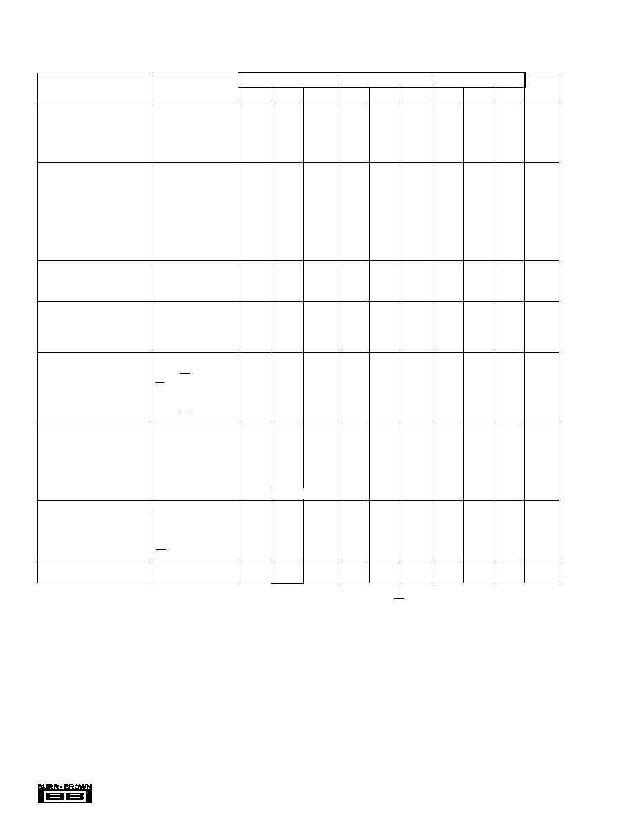
SPECIFICATIONS
At ≠40
∞
C to +85
∞
C, +V
CC
= +5V, V
REF
= +2.5V, f
SAMPLE
= 200kHz, f
CLK
= 16 ∑ f
SAMPLE
, ≠In = +2.5V, unless otherwise specified.
ADS7817
ADS7817B
ADS7817C
PARAMETER
CONDITIONS
MIN
TYP
MAX
MIN
TYP
MAX
MIN
TYP
MAX
UNITS
ANALOG INPUT
Full-Scale Input Span
+In ≠ (≠In)
≠V
REF
+V
REF
T
T
T
T
V
Absolute Input Voltage
+In
≠0.3
V
CC
+0.3
T
T
T
T
V
≠In
≠0.3
4
T
T
T
T
V
Capacitance
15
T
T
pF
Leakage Current
±
1
T
T
µ
A
SYSTEM PERFORMANCE
Resolution
12
T
T
Bits
No Missing Codes
11
12
T
Bits
Integral Linearity Error
±
1
±
2
±
0.8
±
2
±
0.5
±
1
LSB
(1)
Differential Linearity Error
±
1
±
2
±
0.7
±
1
±
0.4
±
1
LSB
Offset Error
±
1
±
6
T
T
T
T
LSB
Gain Error
±
0.5
±
4
T
T
T
T
LSB
Noise
63
T
T
µ
Vrms
Common-Mode Rejection
80
T
T
dB
Power Supply Rejection
82
T
T
dB
SAMPLING DYNAMICS
Conversion Time
12
T
T
Clk Cycles
Acquisition Time
1.5
T
T
Clk Cycles
Throughput Rate
200
T
T
kHz
DYNAMIC CHARACTERISTICS
Total Harmonic Distortion
V
IN
= 5.0Vp-p at 1kHz
≠83
T
T
dB
V
IN
= 5.0Vp-p at 5kHz
≠81
T
T
dB
SINAD
V
IN
= 5.0Vp-p at 1kHz
71
T
T
dB
Spurious Free Dynamic Range
V
IN
= 5.0Vp-p at 1kHz
86
T
T
dB
REFERENCE INPUT
Voltage Range
0.1
2.5
T
T
T
T
V
Resistance
CS = V
CC
5
T
T
G
CS = GND, f
SAMPLE
= 0Hz
5
T
T
G
Current Drain
At Code FF8h
20
100
T
T
T
T
µ
A
f
SAMPLE
= 12.5kHz
1.3
20
T
T
T
T
µ
A
CS = V
CC
0.001
3
T
T
T
T
µ
A
DIGITAL INPUT/OUTPUT
Logic Family
CMOS
T
T
Logic Levels:
V
IH
I
IH
= +5
µ
A
3
+V
CC
+0.3
T
T
T
T
V
V
IL
I
IL
= +5
µ
A
≠0.3
0.8
T
T
T
T
V
V
OH
I
OH
= ≠250
µ
A
3.5
T
T
V
V
OL
I
OL
= 250
µ
A
0.4
T
T
V
Data Format
Binary Two's Complement
T
T
POWER SUPPLY REQUIREMENTS
V
CC
Specified Performance
4.75
5.25
T
T
T
T
V
Quiescent Current
460
800
T
T
T
T
µ
A
f
SAMPLE
= 12.5kHz
(2, 3)
40
T
T
µ
A
f
SAMPLE
= 12.5kHz
(3)
330
T
T
µ
A
Power Down
CS =V
CC
, f
SAMPLE
= 0Hz
3
T
T
µ
A
TEMPERATURE RANGE
Specified Performance
≠40
+85
T
T
T
T
∞
C
T
Specifications same as ADS7817.
NOTE: (1) LSB means Least Significant Bit, with V
REF
equal to +2.5V, one LSB is 1.22mV. (2) f
CLK
= 3.2MHz, CS = V
CC
for 241 clock cycles out of every 256.
(3) See the Power Dissipation section for more information regarding lower sample rates.
The information provided herein is believed to be reliable; however, BURR-BROWN assumes no responsibility for inaccuracies or omissions. BURR-BROWN
assumes no responsibility for the use of this information, and all use of such information shall be entirely at the user's own risk. Prices and specifications are subject
to change without notice. No patent rights or licenses to any of the circuits described herein are implied or granted to any third party. BURR-BROWN does not
authorize or warrant any BURR-BROWN product for use in life support devices and/or systems.
3
Æ
ADS7817
ELECTROSTATIC
DISCHARGE SENSITIVITY
Electrostatic discharge can cause damage ranging from per-
formance degradation to complete device failure. Burr-
Brown Corporation recommends that all integrated circuits
be handled and stored using appropriate ESD protection
methods.
ESD damage can range from subtle performance degrada-
tion to complete device failure. Precision integrated circuits
may be more susceptible to damage because very small
parametric changes could cause the device not to meet
published specifications.
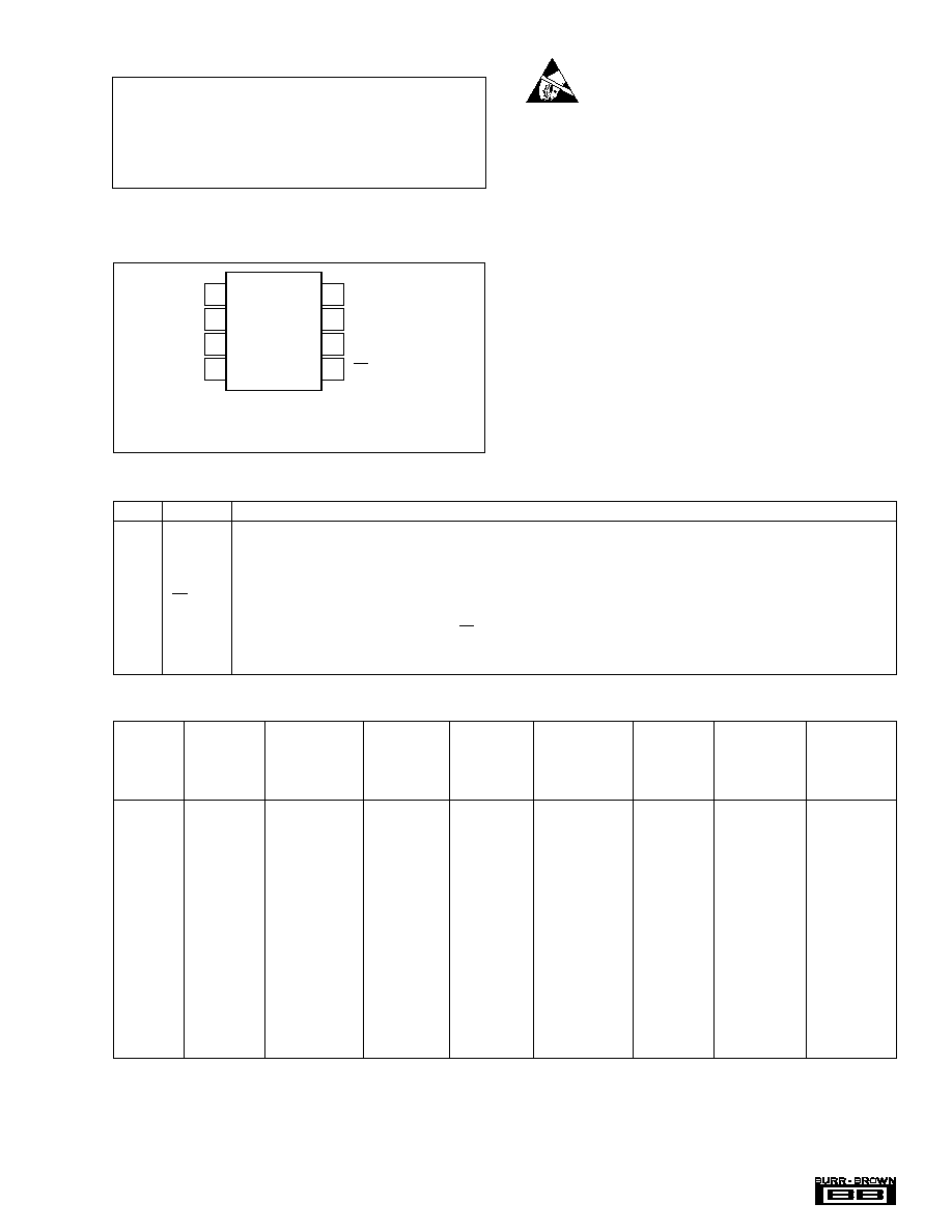
ABSOLUTE MAXIMUM RATINGS
(1)
+V
CC
..................................................................................................... +6V
Analog Input ........................................................... ≠0.3V to (+V
CC
+ 0.3V)
Logic Input ............................................................. ≠0.3V to (+V
CC
+ 0.3V)
Case Temperature ......................................................................... +100
∞
C
Junction Temperature .................................................................... +150
∞
C
Storage Temperature ..................................................................... +125
∞
C
External Reference Voltage .............................................................. +5.5V
NOTE: (1) Stresses above these ratings may permanently damage the device.
PIN CONFIGURATION
PIN ASSIGNMENTS
PIN
NAME
DESCRIPTION
1
V
REF
Reference Input.
2
+In
Non Inverting Input.
3
≠In
Inverting Input.
4
GND
Ground.
5
CS/SHDN
Chip Select when LOW, Shutdown Mode when HIGH.
6
D
OUT
The serial output data word is comprised of 12 bits of data. In operation the data is valid on the falling edge of DCLOCK. The
second clock pulse after the falling edge of CS enables the serial output. After one null bit the data is valid for the next 12 edges.
7
DCLOCK
Data Clock synchronizes the serial data transfer and determines conversion speed.
8
+V
CC
Power Supply.
1
2
3
4
8
7
6
5
+V
CC
DCLOCK
D
OUT
CS/SHDN
V
REF
+In
≠In
GND
ADS7817
PDIP-8,
SOIC-8,
MSOP-8
PACKAGE/ORDERING INFORMATION
MAXIMUM
MAXIMUM
INTEGRAL
DIFFERENTIAL
LINEARITY
LINEARITY
PACKAGE
SPECIFICATION
ERROR
ERROR
DRAWING
TEMPERATURE
PACKAGE
ORDERING
TRANSPORT
PRODUCT
(LSB)
(LSB)
PACKAGE
NUMBER
(1)
RANGE
MARKING
(2)
NUMBER
(3)
MEDIA
ADS7817P
±
2
±
2
MSOP-8
006
≠40
∞
C to +85
∞
C
ADS7817P
ADS7817P
Rails
ADS7817U
±
2
±
2
MSOP-8
182
≠40
∞
C to +85
∞
C
ADS7817U
ADS7817U
"
ADS7817U
"
"
"
"
"
"
ADS7817U/2K5
Tape and Reel
ADS7817E
±
2
±
2
MSOP-8
337
≠40
∞
C to +85
∞
C
A17
ADS7817E
Rails
ADS7817E
"
"
"
"
"
"
ADS7817E/250
Tape and Reel
ADS7817E
"
"
"
"
"
"
ADS7817E/2K5
"
ADS7817PB
±
2
±
1
Plastic DIP-8
006
≠40
∞
C to +85
∞
C
ADS7817PB
ADS7817PB
Rails
ADS7817UB
±
2
±
1
Plastic DIP-8
182
≠40
∞
C to +85
∞
C
ADS7817UB
ADS7817UB
"
ADS7817UB
"
"
"
"
"
"
ADS7817UB/2K5 Tape and Reel
ADS7817EB
±
2
±
1
SOIC-8
337
≠40
∞
C to +85
∞
C
A17
ADS7817EB
Rails
ADS7817EB
"
"
"
"
"
"
ADS7817EB/250
Tape and Reel
ADS7817EB
"
"
"
"
"
"
ADS7817EB/2K5
"
ADS7817PC
±
1
±
0.75
SOIC-8
006
≠40
∞
C to +85
∞
C
ADS7817PC
ADS7817PC
Rails
ADS7817UC
±
1
±
0.75
SOIC-8
182
≠40
∞
C to +85
∞
C
ADS7817UC
ADS7817UC
"
ADS7817UC
"
"
"
"
"
"
ADS7817UC/2K5 Tape and Reel
ADS7817EC
±
1
±
0.75
SOIC-8
337
≠40
∞
C to +85
∞
C
A17
ADS7817EC
Rails
ADS7817EC
"
"
"
"
"
"
ADS7817EC/250
Tape and Reel
ADS7817EC
"
"
"
"
"
"
ADS7817EC/2K5
"
NOTE: (1) For detail drawing and dimension table, please see end of data sheet or Package Drawing File on Web. (2) Performance Grade information is marked
on the reel. (3) Models with a slash(/) are available only in Tape and reel in quantities indicated (e.g. /250 indicates 250 units per reel, /2K5 indicates 2500 devices
per reel). Ordering 2500 pieces of "ADS7817E/2K5" will get a single 2500-piece Tape and Reel. For detailed Tape and Reel mechanical information, refer to the
www.burr-brown.com web site under Applications and Tape and Reel Orientation and Dimensions.
4
Æ
ADS7817
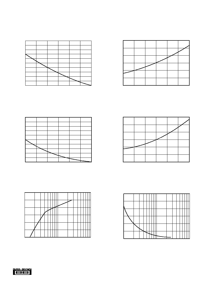
TYPICAL PERFORMANCE CURVES
At T
A
= +25
∞
C, V
CC
= +5V, V
REF
= +2.5V, f
SAMPLE
= 200kHz, and f
CLK
= 16 ∑ f
SAMPLE
, ≠In = +2.5V, unless otherwise specified.
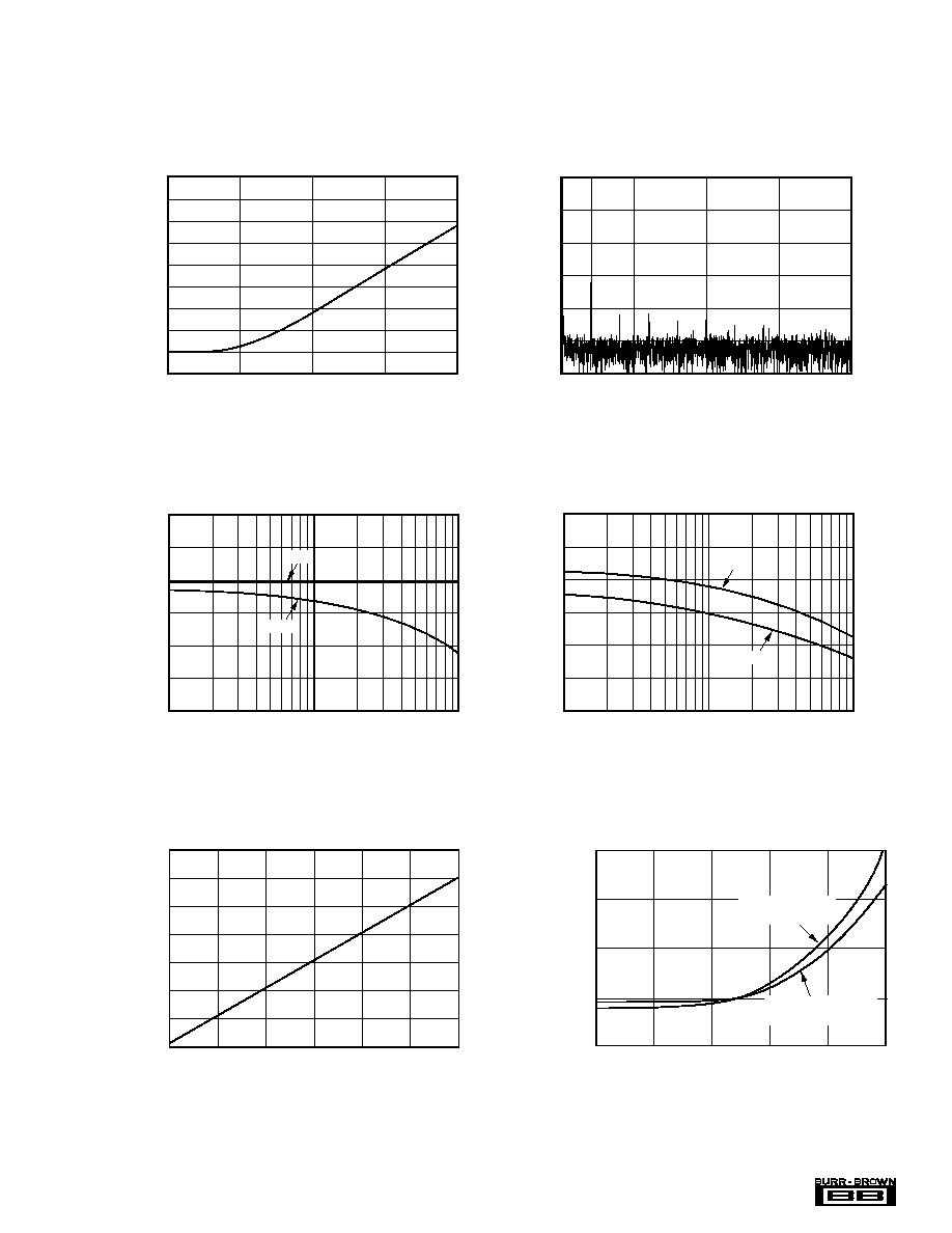
CHANGE IN OFFSET vs REFERENCE VOLTAGE
5
4.5
4
3.5
3
2.5
2
1.5
1
0.5
0
Change in Offset (LSB)
1.0
1.25
1.5
1.75
2.25
2.0
2.5
Reference Voltage (V)
CHANGE IN GAIN vs REFERENCE VOLTAGE
4
3.5
3
2.5
2
1.5
1
0.5
0
Change in Gain (LSB)
Reference Voltage (V)
1.0
1.25
1.5
1.75
2.25
2.0
2.5
CHANGE IN OFFSET vs TEMPERATURE
1.2
0.8
0.4
0.0
≠0.4
≠0.8
≠1.2
Delta from 25∞C (LSB)
≠50
≠25
0
25
50
75
100
Temperature (∞C)
CHANGE IN GAIN vs TEMPERATURE
0.15
0.1
0.05
0
≠0.05
≠0.1
≠0.15
Delta from 25∞C (LSB)
≠50
≠25
0
25
50
75
100
Temperature (∞C)
12.0
11.5
11.0
10.5
10.0
9.5
9.0
EFFECTIVE NUMBER OF BITS
vs REFERENCE VOLTAGE
Reference Voltage
0.1
1
10
Effective Number of Bits
18
15
12
9
6
3
0
PEAK-TO-PEAK NOISE vs REFERENCE VOLTAGE
Reference Voltage
0.1
1
10
Peak-to-Peak Noise (LSB)
5
Æ
ADS7817
TYPICAL PERFORMANCE CURVES
(Cont.)
At T
A
= +25
∞
C, V
CC
= +5V, V
REF
= +2.5V, f
SAMPLE
= 200kHz, and f
CLK
= 16 ∑ f
SAMPLE
, ≠In = +2.5V, unless otherwise specified.
73
72
71
70
69
68
67
SIGNAL-TO-NOISE RATIO AND
SIGNAL-TO-(NOISE+DISTORTION)
vs INPUT FREQUENCY
Input Frequency (kHz)
1
10
100
SNR and SINAD (dB)
SNR
SINAD
80
70
60
50
40
30
20
10
SIGNAL-TO-(NOISE+DISTORTION)
vs INPUT LEVEL
Input Level (dB)
≠60
≠50
≠40
≠30
≠10
≠20
0
SINAD (dB)
POWER SUPPLY REJECTION vs RIPPLE FREQUENCY
0
≠10
≠20
≠30
≠40
≠50
≠60
≠70
≠80
≠90
Power Supply Rejection (dB)
1
10
100
1000
10000
Ripple Frequency (kHz)
FREQUENCY SPECTRUM
(4096 Point FFT; f
IN
= 9.9kHz, ≠0.5dB)
0
≠20
≠40
≠60
≠80
≠100
≠120
Amplitude (dB)
0
25
50
75
100
Frequency (kHz)
95
90
85
80
75
70
65
SPURIOUS FREE DYNAMIC RANGE AND
TOTAL HARMONIC DISTORTION
vs INPUT FREQUENCY
Input Frequency (kHz)
1
10
100
SFDR (dB)
≠95
≠90
≠85
≠80
≠75
≠70
≠65
THD (dB)
SFDR
THD
CHANGE IN INTEGRAL LINEARITY and DIFFERENTIAL
LINEARITY vs SAMPLE RATE
1.5
1.0
0.5
0
≠0.5
Delta from f
SAMPLE
= 200kHz (LSB)
0
80
160
240
320
400
Sample Rate (kHz)
Change in Integral
Linearity (LSB)
Change in Differential
Linearity (LSB)