 | –≠–ª–µ–∫—Ç—Ä–æ–Ω–Ω—ã–π –∫–æ–º–ø–æ–Ω–µ–Ω—Ç: ADS7835 | –°–∫–∞—á–∞—Ç—å:  PDF PDF  ZIP ZIP |
1
ADS7835
Æ
ADS7835
DESCRIPTION
The ADS7835 is a 12-bit, sampling analog-to-digi-
tal converter (A/D) complete with sample-and-hold
(S/H), internal 2.5V reference, and synchronous
serial interface. Typical power dissipation is 17.5mW
at a 500kHz throughput rate. The device can be
placed into a power-down mode which reduces dis-
sipation to just 2.5mW. The input range is ≠V
REF
to
+V
REF
, and the internal reference can be overdriven
by an external voltage.
Low power, small size, and high speed make the
ADS7835 ideal for battery-operated systems such
as wireless communication devices, portable multi-
channel data loggers, and spectrum analyzers. The
serial interface also provides low cost isolation for
remote data acquisition. The ADS7835 is avail-
able in an MSOP-8 package and is guaranteed over
the ≠40
∞
C to +85
∞
C temperature range.
12-Bit, High-Speed, Low Power Sampling
ANALOG-TO-DIGITAL CONVERTER
Æ
FEATURES
q
500kHz THROUGHPUT RATE
q
2.5V INTERNAL REFERENCE
q
LOW POWER: 17.5mW
q
SINGLE SUPPLY +5V OPERATION
q
SERIAL INTERFACE
q
GUARANTEED NO MISSING CODES
q
MSOP-8
q
±
V
REF
INPUT RANGE
APPLICATIONS
q
BATTERY-OPERATED SYSTEMS
q
DIGITAL SIGNAL PROCESSING
q
HIGH-SPEED DATA ACQUISITION
q
WIRELESS COMMUNICATION SYSTEMS
©
1998 Burr-Brown Corporation
PDS-1478B
Printed in U.S.A.May, 2000
International Airport Industrial Park ∑ Mailing Address: PO Box 11400, Tucson, AZ 85734 ∑ Street Address: 6730 S. Tucson Blvd., Tucson, AZ 85706 ∑ Tel: (520) 746-1111
Twx: 910-952-1111 ∑ Internet: http://www.burr-brown.com/ ∑ Cable: BBRCORP ∑ Telex: 066-6491 ∑ FAX: (520) 889-1510 ∑ Immediate Product Info: (800) 548-6132
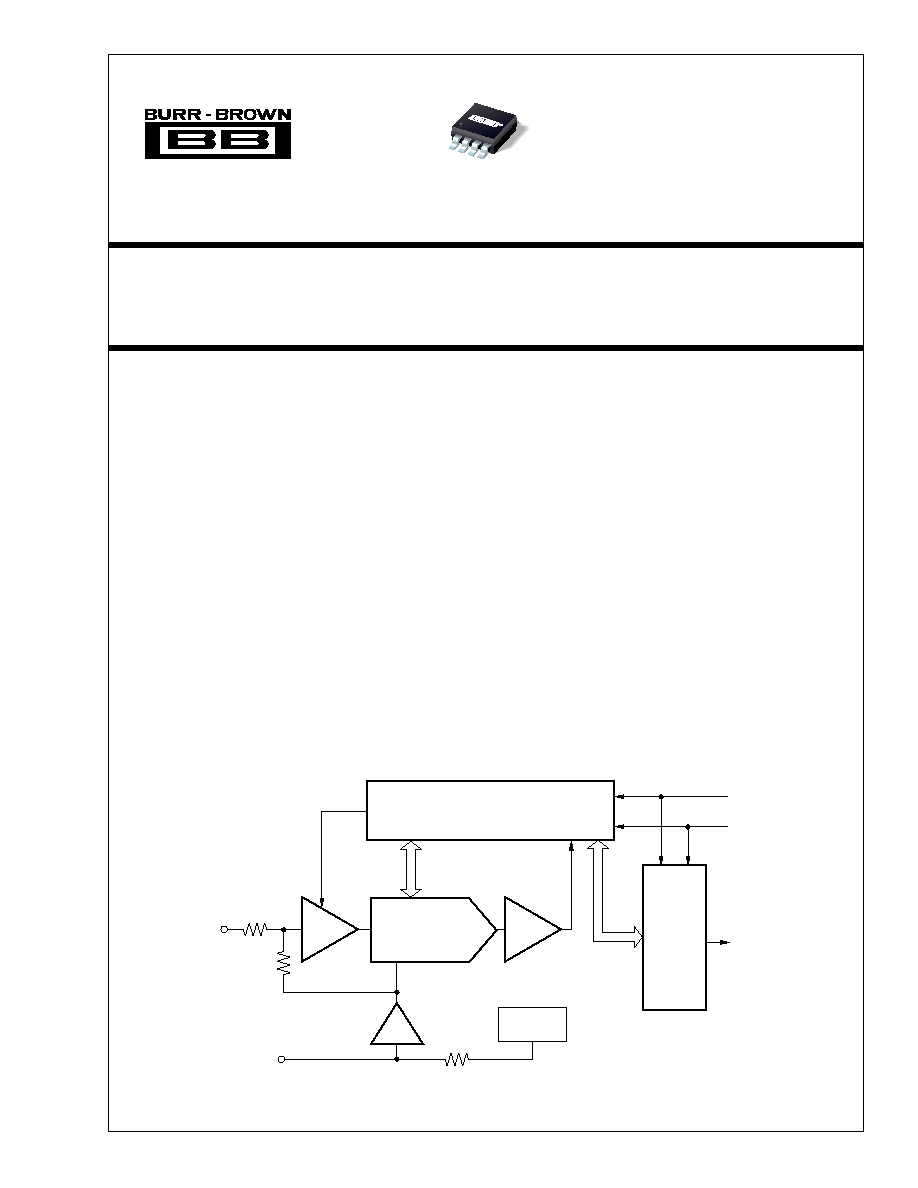
SAR
CLK
Serial
Interface
Comparator
S/H Amp
DATA
±
2.5V
Input
CDAC
Internal
+2.5V Ref
Buffer
V
REF
CONV
10k
±
30%
2k
2k
For most current data sheet and other product
information, visit www.burr-brown.com

2
ADS7835
Æ
SPECIFICATIONS
At T
A
= ≠40
∞
C to +85
∞
C, +V
CC
= +5V, f
SAMPLE
= 500kHz, f
CLK
= 16 ∑ f
SAMPLE
, and internal +2.5V reference, unless otherwise specified.
The information provided herein is believed to be reliable; however, BURR-BROWN assumes no responsibility for inaccuracies or omissions. BURR-BROWN
assumes no responsibility for the use of this information, and all use of such information shall be entirely at the user's own risk. Prices and specifications are subject
to change without notice. No patent rights or licenses to any of the circuits described herein are implied or granted to any third party. BURR-BROWN does not
authorize or warrant any BURR-BROWN product for use in life support devices and/or systems.
ADS7835E
ADS7835EB
PARAMETER
CONDITIONS
MIN
TYP
MAX
MIN
TYP
MAX
UNITS
RESOLUTION
12
T
Bits
ANALOG INPUT
(1)
Input Voltage Range
±
2.5V with the 2.5V
≠V
REF
+V
REF
T
T
V
Internal Reference
Input Capacitance
25
T
pF
Input Resistance
During Conversion (CONV = LOW)
2
T
k
SYSTEM PERFORMANCE
No Missing Codes
12
T
Bits
Integral Linearity
±
1
±
2
±
0.5
±
1
LSB
(2)
Differential Linearity
±
0.8
±
0.5
±
1
LSB
Bipolar Offset Error
±
2
±
10
±
1
±
5
LSB
Positive Fulll-Scale Error
(3)
At 25
∞
C
±
12
±
20
±
7
±
12
LSB
≠40
∞
C to +85
∞
C
±
35
±
25
LSB
Negative Full-Scale Error
(3)
At 25
∞
C
±
12
±
20
±
7
±
12
LSB
≠40
∞
C to +85
∞
C
±
35
±
25
LSB
Noise
200
T
µ
Vrms
Power Supply Rejection Ratio
Worst-Case
, +V
CC
= 5V
±
5%
0.3
T
LSB
SAMPLING DYNAMICS
Conversion Time
1.625
T
µ
s
Acquisition Time
0.350
T
µ
s
Throughput Rate
500
T
kHz
Aperture Delay
5
T
ns
Aperture Jitter
30
T
ps
Step Response
375
T
ns
DYNAMIC CHARACTERISTICS
Signal-to-Noise Ratio
V
IN
= 5Vp-p at 10kHz
72
T
dB
Total Harmonic Distortion
(4)
V
IN
= 5Vp-p at 10kHz
≠78
≠72
≠82
≠75
dB
Signal-to-(Noise+Distortion)
V
IN
= 5Vp-p at 10kHz
68
70
70
72
dB
Spurious Free Dynamic Range
V
IN
= 5Vp-p at 10kHz
72
78
75
82
dB
REFERENCE OUTPUT
Voltage
I
OUT
= 0
2.475
2.50
2.525
2.48
T
2.52
V
Source Current
(5)
Static Load
50
T
µ
A
Line Regulation
4.75V
V
CC
5.25V
0.2
T
mV
REFERENCE INPUT
Range
2.3
2.9
T
T
V
Resistance
(6)
To Internal Reference Voltage
10
T
k
DIGITAL INPUT/OUTPUT
Logic Family
CMOS
T
Logic Levels:
V
IH
I
IH
+5
µ
A
3.0
+V
CC
+ 0.3
T
T
V
V
IL
I
IL
+5
µ
A
≠0.3
0.8
T
T
V
V
OH
I
OH
= ≠500
µ
A
3.5
T
V
V
OL
I
OL
= 500
µ
A
0.4
T
V
Data Format
Binary Two's Complement
T
POWER SUPPLY REQUIREMENT
+V
CC
Specified Performance
4.75
5.25
T
T
V
Quiescent Current
f
SAMPLE
= 500kHz
3.5
T
mA
Power-Down
0.5
T
mA
Power Dissipation
17.5
30
T
T
mW
Power-Down
2.5
T
mW
TEMPERATURE RANGE
Specified Performance
≠40
+85
T
T
∞
C
T
Specifications same as ADS7835E.
NOTES: (1) Ideal input span, does not include gain or offset error. (2) LSB means Least Significant Bit, with V
REF
equal to +2.5V, one LSB is 1.22mV. (3) Measured
relative to an ideal positive full scale of 2.499V for positive full-scale error. Measured relative to an ideal negative full scale of ≠2.499V for negative full-scale error.
(4) Calculated on the first nine harmonics of the input frequency. (5) If the internal reference is required to source current to an external load, the reference voltage
will change due to the internal 10k
resistor. (6) Can vary
±
30%.

3
ADS7835
Æ
+V
CC
to GND ............................................................................ ≠0.3V to 6V
Analog Inputs to GND ............................................................. ≠5.3 to +5.3
Digital Inputs to GND ............................................... ≠0.3V to (V
CC
+ 0.3V)
Power Dissipation .......................................................................... 325mW
Maximum Junction Temperature ................................................... +150
∞
C
Operating Temperature Range ......................................... ≠40
∞
C to +85
∞
C
Storage Temperature Range .......................................... ≠65
∞
C to +150
∞
C
Lead Temperature (soldering, 10s) ............................................... +300
∞
C
NOTE: (1) Stresses above those listed under "Absolute Maximum Ratings" may
cause permanent damage to the device. Exposure to absolute maximum condi-
tions for extended periods may affect device reliability.
ELECTROSTATIC
DISCHARGE SENSITIVITY
Electrostatic discharge can cause damage ranging from per-
formance degradation to complete device failure. Burr-Brown
Corporation recommends that all integrated circuits be
handled and stored using appropriate ESD protection meth-
ods.
ESD damage can range from subtle performance degrada-
tion to complete device failure. Precision integrated circuits
may be more susceptible to damage because very small
parametric changes could cause the device not to meet
published specifications.
ABSOLUTE MAXIMUM RATINGS
(1)
1
2
3
4
8
7
6
5
+V
CC
CLK
DATA
CONV
V
REF
A
IN
GND
GND
ADS7835
MSOP-8
PIN CONFIGURATION
Top View
PIN
NAME
DESCRIPTION
1
V
REF
Reference Output. Decouple to ground with a 0.1
µ
F ceramic capacitor and a 2.2
µ
F tantalum capacitor.
2
A
IN
±
2.5V Input
3
GND
Ground
4
GND
Ground
5
CONV
Convert Input. Controls the sample/hold mode, start of conversion, start of serial data transfer, type of serial transfer, and power-
down mode. See the Digital Interface section for more information.
6
DATA
Serial Data Output. The 12-bit conversion result is serially transmitted most significant bit first with each bit valid on the rising edge
of CLK. By properly controlling the CONV input, it is possibly to have the data transmitted least significant bit first. See the Digital
Interface section for more information.
7
CLK
Clock Input. Synchronizes the serial data transfer and determines conversion speed.
8
+V
CC
Power Supply. Decouple to ground with a 0.1
µ
F ceramic capacitor and a 10
µ
F tantalum capacitor.
PIN ASSIGNMENTS
PACKAGE/ORDERING INFORMATION
MAXIMUM
MAXIMUM
INTEGRAL
DIFFERENTIAL
LINEARITY
LINEARITY
PACKAGE
SPECIFICATION
ERROR
ERROR
DRAWING
TEMPERATURE
PACKAGE
ORDERING
TRANSPORT
PRODUCT
(LSB)
(LSB)
PACKAGE
NUMBER
(1)
RANGE
MARKING
(2)
NUMBER
(3)
MEDIA
ADS7835E
±
2
N/S
(4)
MSOP-8
337
≠40
∞
C to +85
∞
C
B35
ADS7835E/250
Tape and Reel
"
"
"
"
"
"
"
ADS7835E/2K5
Tape and Reel
ADS7835EB
±
1
±
1
MSOP-8
337
≠40
∞
C to +85
∞
C
B35
ADS7835EB/250
Tape and Reel
"
"
"
"
"
"
"
ADS7835EB/2K5
Tape and Reel
ADS7835P
±
2
N/S
(4)
Plastic DIP-8
006
≠40
∞
C to +85
∞
C
ADS7835P
ADS7835P
Rails
ADS7835PB
±
1
±
1
"
"
"
ADS7835PB
ADS7835PB
Rails
NOTE: (1) For detail drawing and dimension table, please see end of data sheet or Package Drawing File on Web. (2) Performance Grade information is marked
on the reel. (3) Models with a slash(/) are available only in Tape and reel in quantities indicated (e.g. /250 indicates 250 units per reel, /2K5 indicates 2500 devices
per reel). Ordering 2500 pieces of "ADS7835E/2K5" will get a single 2500-piece Tape and Reel. For detailed Tape and Reel mechanical information, refer to the
www.burr-brown.com web site under Applications and Tape and Reel Orientation and Dimensions. (4) N/S = Not Specified, typical only. However, 12-Bits no missing
codes is guaranteed over temperature.
4
ADS7835
Æ
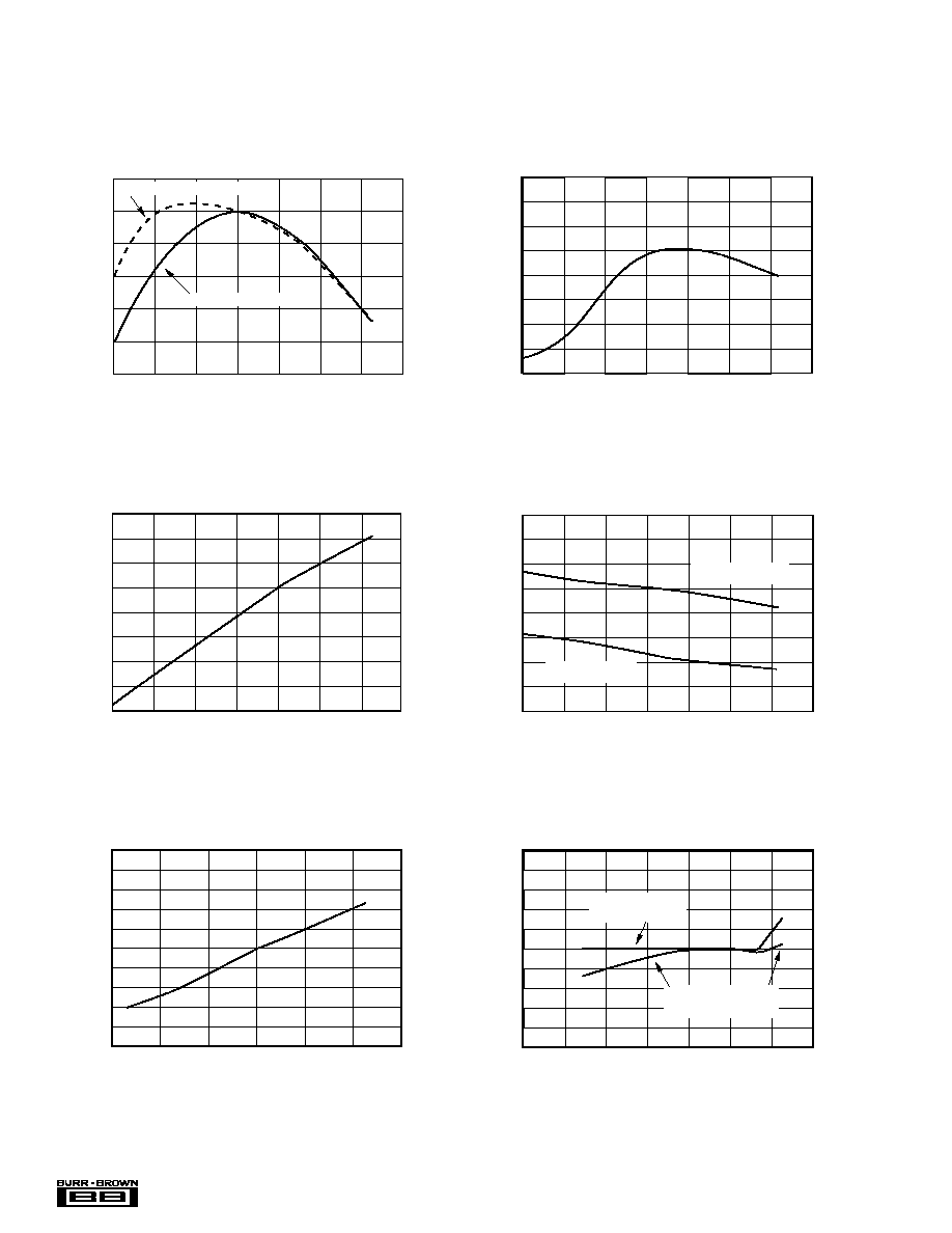
TYPICAL PERFORMANCE CURVES
At T
A
= +25
∞
C, +V
CC
= +5V, f
SAMPLE
= 500kHz, f
CLK
= 16 ∑ f
SAMPLE
, and internal +2.5V reference, unless otherwise specified.
0
60
80
100
≠40
≠20
20
Temperature (
∞
C)
CHANGE IN FULL-SCALE ERRORS
vs TEMPERATURE
Delta from +25
∞
C (LSB)
1.0
0.0
≠1.0
≠2.0
≠3.0
≠4.0
≠5.0
40
Positive Full-Scale Error
Negative Full-Scale Error
CHANGE IN BIPOLAR OFFSET ERROR
vs TEMPERATURE
≠40
100
≠20
0
20
40
Temperature (
∞
C)
Delta from +25
∞
C (LSB)
0.6
0.4
0.2
0.0
≠0.2
≠0.4
≠0.6
≠0.8
≠1.0
60
80
POWER-DOWN SUPPLY CURRENT
vs TEMPERATURE
20
≠40
100
≠20
0
40
Temperature (
∞
C)
Power-Down Supply Current (
µ
A)
470
460
450
440
430
420
410
400
390
60
80
SUPPLY CURRENT vs TEMPERATURE
20
≠40
100
≠20
0
40
Temperature (
∞
C)
Supply Current (mA)
60
80
3.8
3.7
3.6
3.5
3.4
3.3
3.2
3.1
3.0
f
SAMPLE
= 500kHz
f
SAMPLE
= 125kHz
SUPPLY CURRENT vs SAMPLE RATE
100
200
300
400
500
600
700
Sample Rate (kHz)
Supply Current (mA)
4.0
3.9
3.8
3.7
3.6
3.5
3.4
3.3
3.2
3.1
3.0
CHANGE IN INTEGRAL and DIFFERENTIAL LINEARITY
vs SAMPLE RATE
0
100
200
300
400
500
600
700
Sample Rate (kHz)
Delta from f
SAMPLE
= 500kHz (LSB)
0.5
0.4
0.3
0.2
0.1
0.0
≠0.1
≠0.2
≠0.3
≠0.4
≠0.5
Change in Differential
Linearity (LSB)
Change in Integral
Linearity (LSB)

5
ADS7835
Æ
TYPICAL PERFORMANCE CURVES
(Cont.)
At T
A
= +25
∞
C, +V
CC
= +5V, f
SAMPLE
= 500kHz, f
CLK
= 16 ∑ f
SAMPLE
, and internal +2.5V reference, unless otherwise specified.
PEAK-TO-PEAK NOISE
vs EXTERNAL REFERENCE VOLTAGE
2.2
2
2.5
2.1
2.3
External Reference Voltage (V)
Peak-to-Peak Noise (LSB)
0.90
0.85
0.80
0.75
0/70
0.65
0.60
0.55
0.50
2.4
CHANGE END-POINT ERRORS
vs EXTERNAL REFERENCE VOLTAGE
External Reference Voltage (V)
4.0
3.0
2.0
1.0
0.0
≠1.0
≠2.0
≠3.0
≠4.0
≠5.0
Delta from
V
REF
= 2.5V (LSB)
2.2
2.4
2.6
3.0
2.8
Positive Full-Scale Error
and Bipolar Offset Error
Negative Full-Scale Error
POWER SUPPLY REJECTION RATIO
vs POWER SUPPLY RIPPLE FREQUENCY
1
1M
10
100
1k
Power Supply Ripple Frequency (Hz)
Power Supply Rejection Ratio (mV/V)
30
25
20
15
10
5
0
10k
100k
0
0
50
100
150
200
250
Frequency (kHz)
Amplitude (dB)
≠120
≠100
≠80
≠60
≠40
≠20
FREQUENCY SPECTRUM
(4096 Point FFT; f
IN
= 977Hz, ≠0.2dB)
0
≠20
≠40
≠60
≠80
≠100
≠120
0
50
100
150
200
250
Frequency (kHz)
Amplitude (dB)
FREQUENCY SPECTRUM
(4096 Point FFT; f
IN
= 9.77kHz, ≠0.2dB)
0
≠20
≠40
≠60
≠80
≠100
≠120
0
50
100
150
200
250
Frequency (kHz)
Amplitude (dB)
FREQUENCY SPECTRUM
(4096 Point FFT; f
IN
= 99.7kHz, ≠0.2dB)