 | –≠–ª–µ–∫—Ç—Ä–æ–Ω–Ω—ã–π –∫–æ–º–ø–æ–Ω–µ–Ω—Ç: ADS7842E | –°–∫–∞—á–∞—Ç—å:  PDF PDF  ZIP ZIP |

ADS7842
12-Bit, 4-Channel Parallel Output Sampling
ANALOG-TO-DIGITAL CONVERTER
FEATURES
q
SINGLE SUPPLY: 2.7V to 5V
q
4-CHANNEL INPUT MULTIPLEXER
q
UP TO 200kHz SAMPLING RATE
q
FULL 12-BIT PARALLEL INTERFACE
q
±
1 LSB INL AND DNL
q
GUARANTEED NO MISSING CODES
q
72dB SINAD
q
LOW POWER: 2mW
q
SSOP-28 PACKAGE
Æ
DESCRIPTION
The ADS7842 is a complete, 4-channel, 12-bit analog-
to-digital converter (ADC). It contains a 12-bit, ca-
pacitor-based, SAR A/D with a sample-and-hold am-
plifier, interface for microprocessor use and parallel,
three-state output drivers. The ADS7842 is specified
at a 200kHz sampling rate while dissipating only
2mW of power. The reference voltage can be varied
from 100mV to V
CC
with a corresponding LSB reso-
lution from 24
µ
V to 1.22mV. The ADS7842 is guar-
anteed down to 2.7V operation.
Low power, high speed and an on-board multiplexer
make the ADS7842 ideal for battery-operated sys-
tems such as portable, multi-channel dataloggers and
measurement equipment. The ADS7842 is available
in a SSOP-28 package and is guaranteed over the
≠40
∞
C to +85
∞
C temperature range.
©
1998 Burr-Brown Corporation
PDS-1484B
Printed in U.S.A. March, 2000
APPLICATIONS
q
DATA ACQUISITION
q
TEST AND MEASUREMENT
q
INDUSTRIAL PROCESS CONTROL
q
MEDICAL INSTRUMENTS
q
LABORATORY EQUIPMENT
International Airport Industrial Park ∑ Mailing Address: PO Box 11400, Tucson, AZ 85734 ∑ Street Address: 6730 S. Tucson Blvd., Tucson, AZ 85706 ∑ Tel: (520) 746-1111
Twx: 910-952-1111 ∑ Internet: http://www.burr-brown.com/ ∑ Cable: BBRCORP ∑ Telex: 066-6491 ∑ FAX: (520) 889-1510 ∑ Immediate Product Info: (800) 548-6132
ADS7842
SAR
Output
Latches
and
Three
State
Drivers
Three
State
Parallel
Data Bus
Comparator
ADS7842
CS
WR
BUSY
CLK
RD
CDAC
V
REF
4-Channel
MUX
AIN2
AIN1
AIN0
A0
A1
AIN3
For most current data sheet and other product
information, visit www.burr-brown.com

Æ
2
ADS7842
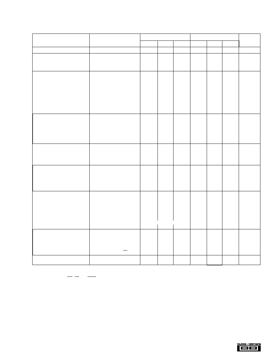
SPECIFICATIONS: +5V
At T
A
= ≠40
∞
C to +85
∞
C, +V
CC
= +5V, V
REF
= +5V, f
SAMPLE
= 200kHz, and f
CLK
= 16 ∑ f
SAMPLE
= 3.2MHz, unless otherwise noted.
The information provided herein is believed to be reliable; however, BURR-BROWN assumes no responsibility for inaccuracies or omissions. BURR-BROWN assumes
no responsibility for the use of this information, and all use of such information shall be entirely at the user's own risk. Prices and specifications are subject to change
without notice. No patent rights or licenses to any of the circuits described herein are implied or granted to any third party. BURR-BROWN does not authorize or warrant
any BURR-BROWN product for use in life support devices and/or systems.
ADS7842E
ADS7842EB
PARAMETER
CONDITIONS
MIN
TYP
MAX
MIN
TYP
MAX
UNITS
RESOLUTION
12
T
Bits
ANALOG INPUT
Full-Scale Input Span
0
V
REF
T
T
V
Capacitance
25
T
pF
Leakage Current
±
1
T
µ
A
SYSTEM PERFORMANCE
No Missing Codes
12
T
Bits
Integral Linearity Error
±
2
±
1
LSB
(1)
Differential Linearity Error
±
0.8
±
0.5
±
1
LSB
Offset Error
±
3
T
LSB
Offset Error Match
0.15
1.0
T
T
LSB
Gain Error
±
4
±
3
LSB
Gain Error Match
0.1
1.0
T
T
LSB
Noise
30
T
µ
Vrms
Power Supply Rejection
70
T
dB
SAMPLING DYNAMICS
Conversion Time
12
T
Clk Cycles
Acquisition Time
3
T
Clk Cycles
Throughput Rate
200
T
kHz
Multiplexer Settling Time
500
T
ns
Aperture Delay
30
T
ns
Aperture Jitter
100
T
ps
DYNAMIC CHARACTERISTICS
Total Harmonic Distortion
(2)
V
IN
= 5Vp-p at 10kHz
≠78
≠72
≠80
≠76
dB
Signal-to-(Noise + Distortion)
V
IN
= 5Vp-p at 10kHz
68
71
70
72
dB
Spurious Free Dynamic Range
V
IN
= 5Vp-p at 10kHz
72
79
76
81
dB
Channel-to-Channel Isolation
V
IN
= 5Vp-p at 50kHz
120
T
dB
REFERENCE INPUT
Range
0.1
+V
CC
T
T
V
Resistance
DCLK Static
5
T
G
Input Current
40
100
T
T
µ
A
f
SAMPLE
= 12.5kHz
2.5
T
µ
A
DCLK Static
0.001
3
T
T
µ
A
DIGITAL INPUT/OUTPUT
Logic Family
CMOS
T
Logic Levels
V
IH
| I
IH
|
+5
µ
A
3.0
5.5
T
T
V
V
IL
| I
IL
|
+5
µ
A
≠0.3
+0.8
T
T
V
V
OH
I
OH
= ≠250
µ
A
3.5
T
V
V
OL
I
OL
= 250
µ
A
0.4
T
V
Data Format
Straight Binary
T
External Clock
0.2
8
T
T
MHz
POWER SUPPLY REQUIREMENTS
+V
CC
Specified Performance
4.75
5.25
T
T
V
Quiescent Current
550
900
T
T
µ
A
f
SAMPLE
= 12.5kHz
300
T
µ
A
Power-Down Mode
(3)
, CS = +V
CC
3
T
µ
A
Power Dissipation
4.5
T
mW
TEMPERATURE RANGE
Specified Performance
≠40
+85
T
T
∞
C
T
Same specifications as ADS7842E.
NOTE: (1) LSB means Least Significant Bit. With V
REF
equal to +5.0V, one LSB is 1.22mV. (2) First five harmonics of the test frequency. (3) Power-down mode at
end of conversion when WR, CS, and BUSY conditions have all been met. Refer to Table III of this data sheet.
Æ
3
ADS7842
SPECIFICATION: +2.7V
At T
A
= ≠40
∞
C to +85
∞
C, +V
CC
= +2.7V, V
REF
= +2.5V, f
SAMPLE
= 125kHz, and f
CLK
= 16 ∑ f
SAMPLE
= 2MHz, unless otherwise noted.
ADS7842E
ADS7842EB
T
Same specifications as ADS7842E.
NOTE: (1) LSB means Least Significant Bit. With V
REF
equal to +2.5V, one LSB is 610mV. (2) First five harmonics of the test frequency. (3) Power-down mode at
end of conversion when WR, CS, and BUSY conditions have all been met. Refer to Table III of this data sheet.
PARAMETER
CONDITIONS
MIN
TYP
MAX
MIN
TYP
MAX
UNITS
RESOLUTION
12
T
Bits
ANALOG INPUT
Full-Scale Input Span
0
V
REF
T
T
V
Capacitance
25
T
pF
Leakage Current
±
1
T
µ
A
SYSTEM PERFORMANCE
No Missing Codes
12
T
Bits
Integral Linearity Error
±
2
±
1
LSB
(1)
Differential Linearity Error
±
0.8
±
0.5
±
1
LSB
Offset Error
±
5
T
LSB
Offset Error Match
0.15
1.0
T
T
LSB
Gain Error
±
4
±
3
LSB
Gain Error Match
0.1
1.0
T
T
LSB
Noise
30
T
µ
Vrms
Power Supply Rejection
70
T
dB
SAMPLING DYNAMICS
Conversion Time
12
T
Clk Cycles
Acquisition Time
3
T
Clk Cycles
Throughput Rate
125
T
kHz
Multiplexer Settling Time
500
T
ns
Aperture Delay
30
T
ns
Aperture Jitter
100
T
ps
DYNAMIC CHARACTERISTICS
Total Harmonic Distortion
(2)
V
IN
= 2.5Vp-p at 10kHz
≠77
≠70
≠79
≠74
dB
Signal-to-(Noise + Distortion)
V
IN
= 2.5Vp-p at 10kHz
68
71
70
72
dB
Spurious Free Dynamic Range
V
IN
= 2.5Vp-p at 10kHz
72
78
76
80
dB
Channel-to-Channel Isolation
V
IN
= 2.5Vp-p at 50kHz
100
T
dB
REFERENCE INPUT
Range
0.1
+V
CC
T
T
V
Resistance
DCLK Static
5
T
G
Input Current
13
40
T
T
µ
A
f
SAMPLE
= 12.5kHz
2.5
T
µ
A
DCLK Static
0.001
3
T
T
µ
A
DIGITAL INPUT/OUTPUT
Logic Family
CMOS
T
Logic Levels
V
IH
| I
IH
|
+5
µ
A
+V
CC
∑ 0.7
5.5
T
T
V
V
IL
| I
IL
|
+5
µ
A
≠0.3
+0.8
T
T
V
V
OH
I
OH
= ≠250
µ
A
+V
CC
∑ 0.8
T
V
V
OL
I
OL
= 250
µ
A
0.4
T
V
Data Format
Straight Binary
T
External Clock
0.2
8
T
T
MHz
POWER SUPPLY REQUIREMENTS
+V
CC
Specified Performance
2.7
3.6
T
T
V
Quiescent Current
280
650
T
T
µ
A
f
SAMPLE
= 12.5kHz
220
T
µ
A
Power-Down Mode
(3)
, CS = +V
CC
3
T
µ
A
Power Dissipation
1.8
T
mW
TEMPERATURE RANGE
Specified Performance
≠40
+85
T
T
∞
C
Æ
4
ADS7842
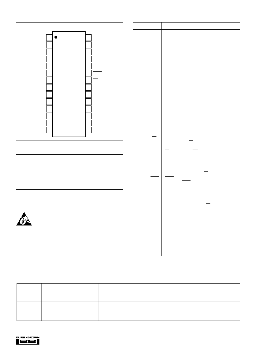
PIN CONFIGURATION
Top View
SSOP
PIN DESCRIPTIONS
PIN
NAME
DESCRIPTION
1
AIN0
Analog Input Channel 0
2
AIN1
Analog Input Channel 1
3
AIN2
Analog Input Channel 2
4
AIN3
Analog Input Channel 3
5
V
REF
Voltage Reference Input. See Specifications Tables
for ranges.
6
AGND
Analog Ground
7
DB11
Data Bit 11 (MSB)
8
DB10
Data Bit 10
9
DB9
Data Bit 9
10
DB8
Data Bit 8
11
DB7
Data Bit 7
12
DB6
Data Bit 6
13
DB5
Data Bit 5
14
DGND
Digital Ground
15
DB4
Data Bit 4
16
DB3
Data Bit 3
17
DB2
Data Bit 2
18
DB1
Data Bit 1
19
DB0
Data Bit 0 (LSB)
20
RD
Read Input. Active LOW. Reads the data outputs in
combination with CS.
21
CS
Chip Select Input. Active LOW. The combination of
CS taken LOW and WR taken LOW initiates a new
conversion and places the outputs in the tri-state
mode.
22
WR
Write Input. Active LOW. Starts a new conversion
and selects an analog channel via address inputs A0
and A1, in combination with CS.
23
BUSY
BUSY goes LOW and stays LOW during a
conversion. BUSY rises when a conversion is
complete and enables the parallel outputs.
24
CLK
External Clock Input. The clock speed determines the
conversion rate by the equation f
CLK
= 16 ∑ f
SAMPLE
.
25, 26
A0, A1
Address Inputs. Selects one of four analog input
channels in combination with CS and WR. The
address inputs are latched on the rising edge of
either RD or WR.
A0
A1
Channel Selected
0
0
AIN0
0
1
AIN1
1
0
AIN2
1
1
AIN3
27
V
DIG
Digital Supply Input. Nominally +5V.
28
V
ANA
Analog Supply Input. Nominally +5V.
ABSOLUTE MAXIMUM RATINGS
(1)
+V
CC
to GND ........................................................................ ≠0.3V to +6V
Analog Inputs to GND ............................................ ≠0.3V to +V
CC
+ 0.3V
Digital Inputs to GND ........................................................... ≠0.3V to +6V
Power Dissipation .......................................................................... 250mW
Maximum Junction Temperature ................................................... +150
∞
C
Operating Temperature Range ........................................ ≠40
∞
C to +85
∞
C
Storage Temperature Range ......................................... ≠65
∞
C to +150
∞
C
Lead Temperature (soldering, 10s) ............................................... +300
∞
C
NOTE: (1) Stresses above those listed under "Absolute Maximum Ratings"
may cause permanent damage to the device. Exposure to absolute maximum
conditions for extended periods may affect device reliability.
ELECTROSTATIC
DISCHARGE SENSITIVITY
This integrated circuit can be damaged by ESD. Burr-Brown recom-
mends that all integrated circuits be handled with
appropriate precautions. Failure to observe proper handling and
installation procedures can cause damage.
ESD damage can range from subtle performance degradation to
complete device failure. Precision integrated circuits may be more
susceptible to damage because very small parametric changes could
cause the device not to meet its published specifications.
MINIMUM
RELATIVE
SPECIFICATION
PACKAGE
ACCURACY
SINAD
TEMPERATURE
DRAWING
ORDERING
TRANSPORT
PRODUCT
(LSB)
(dB)
RANGE
PACKAGE
NUMBER
NUMBER
(1)
MEDIA
ADS7842E
±
2
68
≠40
∞
C to +85
∞
C
SSOP-28
324
ADS7842E
Rails
"
"
"
"
"
"
ADS7842E/1K
Tape and Reel
ADS7842EB
±
1
70
≠40
∞
C to +85
∞
C
SSOP-28
324
ADS7842EB
Rails
"
"
"
"
"
"
ADS7842EB/1K
Tape and Reel
NOTES: (1) Models with a slash (/) are available only in Tape and Reel in the quantities indicated (e.g., /1K indicates 1000 devices per reel). Ordering 1000 pieces
of "ADS7842E/1K" will get a single 1000-piece Tape and Reel.
PACKAGE/ORDERING INFORMATION
1
2
3
4
5
6
7
8
8
10
11
12
13
14
AIN0
AIN1
AIN2
AIN3
V
REF
AGND
DB11
DB10
DB9
DB8
DB7
DB6
DB5
DGND
V
ANA
V
DIG
A1
A0
CLK
BUSY
WR
CS
RD
DB0
DB1
DB2
DB3
DB4
28
27
26
25
24
23
22
21
20
19
18
17
16
15
ADS7842E
Æ
5
ADS7842
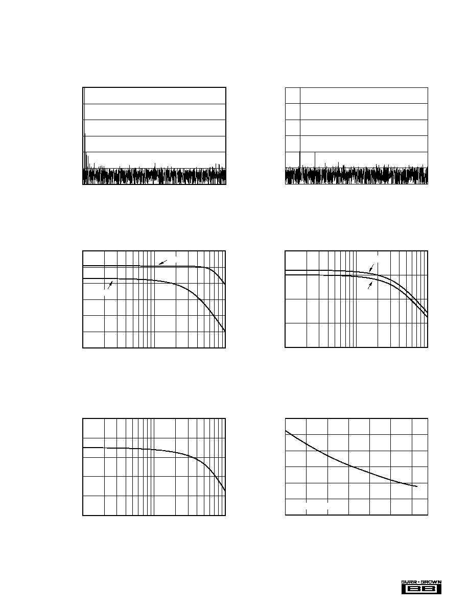
TYPICAL PERFORMANCE CURVES: +5V
At T
A
= +25
∞
C, +V
CC
= +5V, V
REF
= +5V, f
SAMPLE
= 200kHz, and f
CLK
= 16 ∑ f
SAMPLE
= 3.2MHz, unless otherwise noted.
0
≠20
≠40
≠60
≠80
≠100
≠120
FREQUENCY SPECTRUM
(4096 Point FFT; fIN = 1,123Hz, ≠0.2dB)
0
100
25
75
50
Frequency (kHz)
Amplitude (dB)
0
≠20
≠40
≠60
≠80
≠100
≠120
FREQUENCY SPECTRUM
(4096 Point FFT; fIN = 10.3kHz, ≠0.2dB)
0
100
25
75
50
Frequency (kHz)
Amplitude (dB)
SIGNAL-TO-NOISE RATIO AND SIGNAL-TO-
(NOISE+DISTORTION) vs INPUT FREQUENCY
10
1
100
Input Frequency (kHz)
SNR and SINAD (dB)
74
73
72
71
70
69
68
SINAD
SNR
SPURIOUS FREE DYNAMIC RANGE AND TOTAL
HARMONIC DISTORTION vs INPUT FREQUENCY
10
1
100
Input Frequency (kHz)
SFDR (dB)
THD (dB)
85
80
75
70
65
≠85
≠80
≠75
≠70
≠65
THD
SFDR
12.0
11.8
11.6
11.4
11.2
11.0
EFFECTIVE NUMBER OF BITS
vs INPUT FREQUENCY
10
1
100
Input Frequency (kHz)
Effective Number of Bits
CHANGE IN SIGNAL-TO-(NOISE+DISTORTION)
vs TEMPERATURE
≠20
≠40
100
Temperature (
∞
C)
Delta from +25
∞
C (dB)
0.4
0.2
0.0
≠0.2
≠0.4
≠0.6
0.6
0
20
40
60
80
f
IN
= 10kHz, ≠0.2dB