Document Outline
- FEATURES
- APPLICATIONS
- DESCRIPTION
- ABSOLUTE MAXIMUM RATINGS(1)
- PACKAGE/ORDERING INFORMATION(1)
- ELECTRICAL CHARACTERISTICS
- PIN CONFIGURATION
- PIN DESCRIPTION
- TYPICAL CHARACTERISTICS
- THEORY OF OPERATION
- ANALOG INPUT
- INTERNAL REFERENCE
- REFERENCE INPUT
- TOUCH SCREEN SETTLING
- TEMPERATURE MEASUREMENT
- BATTERY MEASUREMENT
- PRESSURE MEASUREMENT
- DIGITAL INTERFACE
- Control Byte
- 16 Clocks-per-Conversion
- Digital Timing
- 15 Clocks-per-Conversion
- Data Format
- 8-Bit Conversion
- POWER DISSIPATION
- LAYOUT

FEATURES
q
SAME PINOUT AS ADS7843
q
2.2V TO 5.25V OPERATION
q
INTERNAL 2.5V REFERENCE
q
DIRECT BATTERY MEASUREMENT (0V to 6V)
q
ON-CHIP TEMPERATURE MEASUREMENT
q
TOUCH-PRESSURE MEASUREMENT
q
QSPI
TM
/SPI
TM
3-WIRE INTERFACE
q
AUTO POWER-DOWN
q
TSSOP-16, SSOP-16, QFN-16,
AND VFBGA-48 PACKAGES
APPLICATIONS
q
PERSONAL DIGITAL ASSISTANTS
q
PORTABLE INSTRUMENTS
q
POINT-OF-SALE TERMINALS
q
PAGERS
q
TOUCH SCREEN MONITORS
q
CELLULAR PHONES
TOUCH SCREEN CONTROLLER
DESCRIPTION
The ADS7846 is a next-generation version to the industry
standard ADS7843 4-wire touch screen controller. The
ADS7846 is 100% pin-compatible with the existing ADS7843,
and drops into the same socket. This allows for easy upgrade
of current applications to the new version. Only software
changes are required to take advantage of the added fea-
tures of direct battery measurement, temperature measure-
ment, and touch-pressure measurement. The ADS7846 also
has an on-chip 2.5V reference that can be used for the
auxiliary input, battery monitor, and temperature measure-
ment modes. The reference can also be powered down when
not used to conserve power. The internal reference operates
down to 2.7V supply voltage while monitoring the battery
voltage from 0V to 6V.
The low-power consumption of < 0.75mW (typ at 2.7V,
reference off), high speed (up to 125kHz clock rate), and on-
chip drivers make the ADS7846 an ideal choice for battery-
operated systems such as personal digital assistants (PDAs)
with resistive touch screens, pagers, cellular phones, and
other portable equipment. The ADS7846 is available in the
small TSSOP-16, SSOP-16, QFN-16, and VFBGA-48 pack-
ages and is specified over the ≠40
∞
C to +85
∞
C temperature
range.
CDAC
Internal 2.5V
Reference
SAR
ADS7846
Comparator
6-Channel
MUX
Serial
Data
Out
Temperature
Sensor
Battery
Monitor
DOUT
BUSY
CS
DCLK
DIN
V
BAT
AUX
V
REF
+V
CC
X+
X≠
Y+
Y≠
PENIRQ
ADS7846
SBAS125H ≠ SEPTEMBER 1999 ≠ REVISED JANUARY 2005
www.ti.com
PRODUCTION DATA information is current as of publication date.
Products conform to specifications per the terms of Texas Instruments
standard warranty. Production processing does not necessarily include
testing of all parameters.
Copyright © 1999-2005, Texas Instruments Incorporated
US Patent No. 6246394
QSPI and SPI are registered trademarks of Motorola.
Æ
ADS7
846
ADS
7846
ADS
7846
Please be aware that an important notice concerning availability, standard warranty, and use in critical applications of
Texas Instruments semiconductor products and disclaimers thereto appears at the end of this data sheet.
All trademarks are the property of their respective owners.
ADS7846
2
SBAS125H
www.ti.com
ABSOLUTE MAXIMUM RATINGS
(1)
+V
CC
to GND ........................................................................ ≠0.3V to +6V
Analog Inputs to GND ............................................ ≠0.3V to +V
CC
+ 0.3V
Digital Inputs to GND ............................................. ≠0.3V to +V
CC
+ 0.3V
Power Dissipation .......................................................................... 250mW
Maximum Junction Temperature ................................................... +150
∞
C
Operating Temperature Range ........................................ ≠40
∞
C to +85
∞
C
Storage Temperature Range ......................................... ≠65
∞
C to +150
∞
C
Lead Temperature (soldering, 10s) ............................................... +300
∞
C
NOTE: (1) Stresses above these ratings can cause permanent damage.
Exposure to absolute maximum conditions for extended periods may degrade
device reliability.
MAXIMUM
INTEGRAL
SPECIFIED
LINEARITY
PACKAGE
TEMPERATURE
PACKAGE
ORDERING
PRODUCT
ERROR (LSB)
PACKAGE-LEAD
DESIGNATOR
RANGE
MARKING
NUMBER
ADS7846E
±
2
SSOP-16
DBQ
≠40
∞
C to +85
∞
C
ADS7846E
ADS7846E
"
"
"
"
"
"
ADS7846E/2K5
ADS7846N
±
2
TSSOP-16
PW
≠40
∞
C to +85
∞
C
ADS7846N
ADS7846N
"
"
"
"
"
"
ADS7846N/2K5
"
"
"
"
"
"
ADS7846N/2K5G4
ADS7846I
±
2
VFBGA-48
GQC
≠40
∞
C to +85
∞
C
ADS7846
ADS7846IGQCR
ADS7846I
±
2
QFN-16
RGV
≠40
∞
C to +85
∞
C
ADS7846
ADS7846IRGVT
"
"
"
"
"
"
ADS7846IRGVR
NOTE: (1) For the most current package and ordering information, see the Package Option Addendum located at the end of this data sheet, or see the TI web site
at www.ti.com.
PACKAGE/ORDERING INFORMATION
(1)
ELECTROSTATIC
DISCHARGE SENSITIVITY
This integrated circuit can be damaged by ESD. Texas Instru-
ments recommends that all integrated circuits be handled with
appropriate precautions. Failure to observe proper handling
and installation procedures can cause damage.
ESD damage can range from subtle performance degradation
to complete device failure. Precision integrated circuits may be
more susceptible to damage because very small parametric
changes could cause the device not to meet its published
specifications.
ADS7846
3
SBAS125H
www.ti.com
ANALOG INPUT
Full-Scale Input Span
Positive Input-Negative Input
0
V
REF
V
Absolute Input Range
Positive Input
≠0.2
+V
CC
+ 0.2
V
Negative Input
≠0.2
+0.2
V
Capacitance
25
pF
Leakage Current
0.1
µ
A
SYSTEM PERFORMANCE
Resolution
12
Bits
No Missing Codes
11
Bits
Integral Linearity Error
±
2
LSB
(1)
Offset Error
±
6
LSB
Gain Error
External V
REF
±
4
LSB
Noise
Including Internal V
REF
70
µ
Vrms
Power-Supply Rejection
70
dB
SAMPLING DYNAMICS
Conversion Time
12
CLK Cycles
Acquisition Time
3
CLK Cycles
Throughput Rate
125
kHz
Multiplexer Settling Time
500
ns
Aperture Delay
30
ns
Aperture Jitter
100
ps
Channel-to-Channel Isolation
V
IN
= 2.5Vp-p at 50kHz
100
dB
SWITCH DRIVERS
On-Resistance
Y+, X+
5
Y≠, X≠
6
Drive Current
(2)
Duration 100ms
50
mA
REFERENCE OUTPUT
Internal Reference Voltage
2.45
2.50
2.55
V
Internal Reference Drift
15
ppm/
∞
C
Quiescent Current
500
µ
A
REFERENCE INPUT
Range
1.0
+V
CC
V
Input Impedance
SER/DFR = 0, PD1 = 0,
1
G
Internal Reference Off
Internal Reference On
250
BATTERY MONITOR
Input Voltage Range
0.5
6.0
V
Input Impedance
Sampling Battery
10
k
Battery Monitor Off
1
G
Accuracy
External V
REF
= 2.5V
≠2
+2
%
Internal Reference
≠3
+3
%
TEMPERATURE MEASUREMENT
Temperature Range
≠40
+85
∞
C
Resolution
Differential Method
(3)
1.6
∞
C
TEMP0
(4)
0.3
∞
C
Accuracy
Differential Method
(3)
±
2
∞
C
TEMP0
(4)
±
3
∞
C
DIGITAL INPUT/OUTPUT
Logic Family
CMOS
Logic Levels, Except PENIRQ
V
IH
| I
IH
|
+5
µ
A
+V
CC
∑ 0.7
+V
CC
+ 0.3
V
IL
| I
IL
|
+5
µ
A
≠0.3
+0.8
V
V
OH
I
OH
= ≠250
µ
A
+V
CC
∑ 0.8
V
V
OL
I
OL
= 250
µ
A
0.4
V
PENIRQ
V
OL
T
A
= 0
∞
C to +85
∞
C, 50k
Pull-Up
0.8
V
Data Format
Straight Binary
POWER-SUPPLY REQUIREMENTS
+V
CC
(5)
Specified Performance
2.7
3.6
V
Operating Range
2.2
5.25
V
Quiescent Current
Internal Reference Off
280
650
µ
A
Internal Reference On
780
µ
A
f
SAMPLE
= 12.5kHz
220
µ
A
Power-Down Mode with
3
µ
A
CS = DCLK = DIN = +V
CC
Power Dissipation
+V
CC
= +2.7V
1.8
mW
TEMPERATURE RANGE
Specified Performance
≠40
+85
∞
C
NOTES: (1) LSB means least significant bit. With V
REF
equal to +2.5V, one LSB is 610
µ
V. (2) Ensured by design, but not tested. Exceeding 50mA source current
may result in device degradation. (3) Difference between TEMP0 and TEMP1 measurement. No calibration necessary. (4) Temperature drift is ≠2.1mV/
∞
C.
(5) ADS7846 operates down to 2.2V.
ADS7846E
PARAMETER
CONDITIONS
MIN
TYP
MAX
UNITS
ELECTRICAL CHARACTERISTICS
At T
A
= ≠40
∞
C to +85
∞
C, +V
CC
= +2.7V, V
REF
= 2.5V internal voltage, f
SAMPLE
= 125kHz, f
CLK
= 16 ∑ f
SAMPLE
= 2MHz, 12-bit mode, and digital inputs = GND or +V
CC
,
unless otherwise noted.
ADS7846
4
SBAS125H
www.ti.com
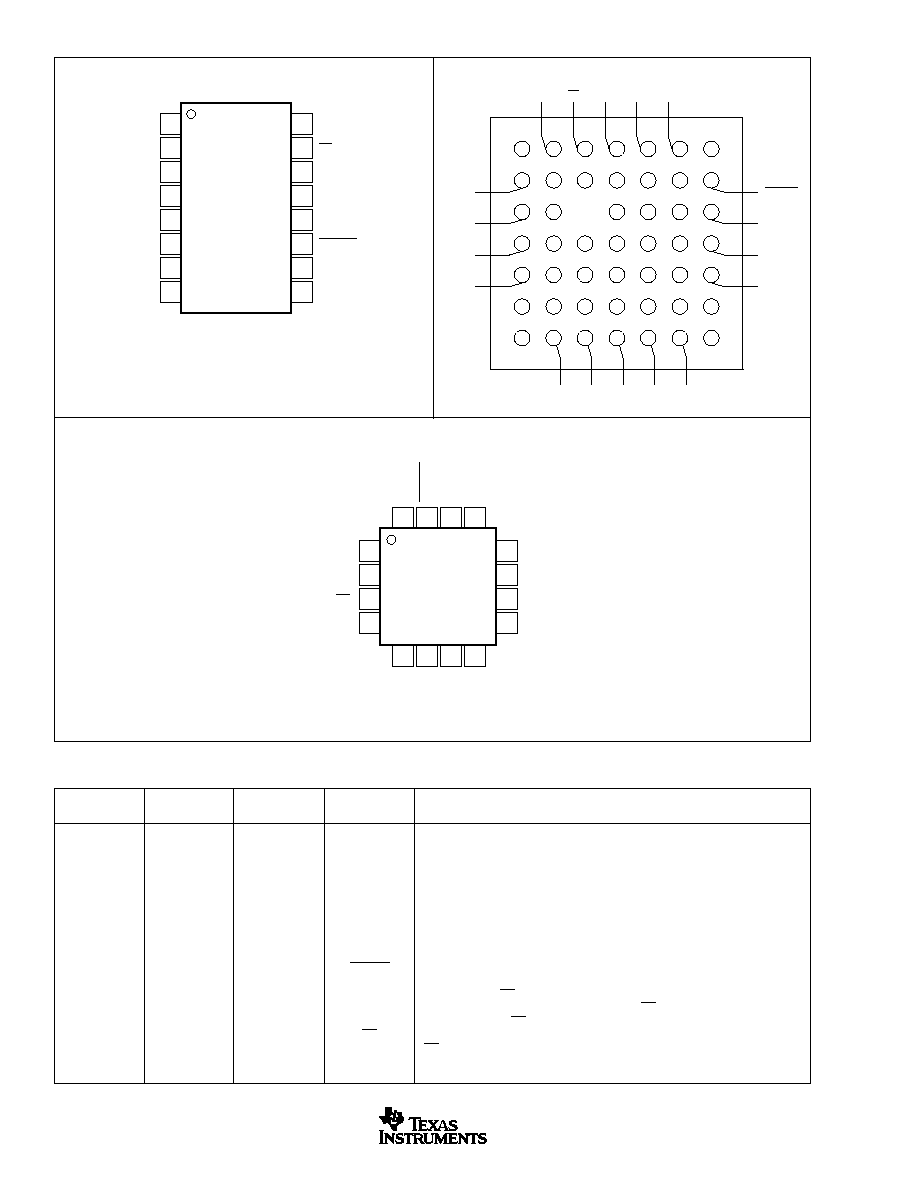
PIN CONFIGURATION
Top View
SSOP, TSSOP
Top View
VFBGA
1
2
3
4
5
6
7
8
+V
CC
X+
Y+
X≠
Y≠
GND
V
BAT
AUX
DCLK
CS
DIN
BUSY
DOUT
PENIRQ
+V
CC
V
REF
16
15
14
13
12
11
10
9
ADS7846
NC
NC
A
2
1
3
4
5
6
7
DCLK
+V
CC
+V
CC
X+
Y+
PENIRQ
+V
CC
V
REF
AUX
CS
DIN
BUSY DOUT
X≠
Y≠
GND
GND
V
BAT
NC
NC
NC
NC
NC
B
C
D
E
F
NC
NC
NC
NC
NC
NC
NC
NC
NC
NC
NC
NC
NC
NC
NC
NC
NC
NC
NC
NC
NC
NC
NC
G
BUSY
DIN
CS
DCLK
AUX
V
BAT
GND
Y≠
1
2
3
4
12
11
10
9
ADS7846
DOUT
PENIRQ
+V
CC
V
REF
16
15
14
13
+V
CC
X+
Y+
X
≠
5
6
7
8
Top View
QFN
SSOP AND
TSSOP PIN #
VFBGA PIN #
QFN PIN #
NAME
DESCRIPTION
1
B1 and C1
5
+V
CC
Power Supply
2
D1
6
X+
X+ Position Input
3
E1
7
Y+
Y+ Position Input
4
G2
8
X≠
X≠ Position Input
5
G3
9
Y≠
Y≠ Position Input
6
G4 and G5
10
GND
Ground
7
G6
11
V
BAT
Battery Monitor Input
8
E7
12
AUX
Auxiliary Input to ADC
9
D7
13
V
REF
Voltage Reference Input/Output
10
C7
14
+V
CC
Digital I/O Power Supply
11
B7
15
PENIRQ
Pen Interrupt. Open anode output (requires 10k
to 100k
pull-up resistor externally).
12
A6
16
DOUT
Serial Data Output. Data is shifted on the falling edge of DCLK. This output is high
impedance when CS is high.
13
A5
1
BUSY
Busy Output. This output is high impedance when CS is high.
14
A4
2
DIN
Serial Data Input. If CS is low, data is latched on rising edge of DCLK.
15
A3
3
CS
Chip Select Input. Controls conversion timing and enables the serial input/output register.
CS high = power-down mode (ADC only).
16
A2
4
DCLK
External Clock Input. This clock runs the SAR conversion process and synchronizes serial data
I/O.
PIN DESCRIPTION
ADS7846
5
SBAS125H
www.ti.com
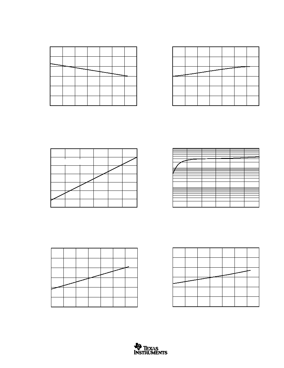
TYPICAL CHARACTERISTICS
At T
A
= +25
∞
C, +V
CC
= +2.7V, V
REF
= External +2.5V, f
SAMPLE
= 125kHz, and f
CLK
= 16 ∑ f
SAMPLE
= 2MHz, unless otherwise noted.
SUPPLY CURRENT vs TEMPERATURE
20
≠40
100
≠20
0
40
Temperature (
∞
C)
Supply Current (
µ
A)
400
350
300
250
200
150
100
60
80
POWER-DOWN SUPPLY CURRENT
vs TEMPERATURE
20
≠40
100
≠20
0
40
Temperature (
∞
C)
Supply Current (nA)
140
120
100
80
60
40
20
60
80
SUPPLY CURRENT vs +V
CC
3.5
2.0
5.0
2.5
4.0
+V
CC
(V)
Supply Current (
µ
A)
390
370
350
330
310
290
270
250
4.5
3.0
f
SAMPLE
= 12.5kHz
MAXIMUM SAMPLE RATE vs +V
CC
3.5
2.0
5.0
2.5
4.0
+V
CC
(V)
Sample Rate (Hz)
1M
100k
10k
1k
4.5
3.0
CHANGE IN GAIN vs TEMPERATURE
20
≠40
100
≠20
0
40
Temperature (
∞
C)
Delta from +25
∞
C (LSB)
0.15
0.10
0.05
0
≠0.05
≠0.10
≠0.15
60
80
CHANGE IN OFFSET vs TEMPERATURE
20
≠40
100
≠20
0
40
Temperature (
∞
C)
Delta from +25
∞
C (LSB)
0.6
0.4
0.2
0
≠0.2
≠0.4
≠0.6
60
80