 | –≠–ª–µ–∫—Ç—Ä–æ–Ω–Ω—ã–π –∫–æ–º–ø–æ–Ω–µ–Ω—Ç: ADS7864Y | –°–∫–∞—á–∞—Ç—å:  PDF PDF  ZIP ZIP |

1
ADS7864
Æ
500kHz, 12-Bit, 6-Channel
Simultaneous Sampling
ANALOG-TO-DIGITAL CONVERTER
FEATURES
q
6 SIMULTANEOUS SAMPLING CHANNELS
q
FULLY DIFFERENTIAL INPUTS
q
2
µ
s TOTAL THROUGHPUT PER CHANNEL
q
GUARANTEED NO MISSING CODES
q
PARALLEL INTERFACE
q
1MHz EFFECTIVE SAMPLING RATE
q
LOW POWER: 50mW
q
6X FIFO
APPLICATIONS
q
MOTOR CONTROL
q
MULTI-AXIS POSITIONING SYSTEMS
q
3-PHASE POWER CONTROL
DESCRIPTION
The ADS7864 is a dual 12-bit, 500kHz Analog-to-
Digital (A/D) converter with 6 fully differential input
channels grouped into three pairs for high speed simul-
taneous signal acquisition. Inputs to the sample-and-
hold amplifiers are fully differential and are main-
tained differential to the input of the A/D converter.
This provides excellent common-mode rejection of
80dB at 50kHz which is important in high noise
environments.
The ADS7864 offers a parallel interface and control
inputs to minimize software overhead. The output data
for each channel is available as a 16-bit word (address
and data). The ADS7864 is offered in a TQFP-48
package and is fully specified over the ≠40
∞
C to +85
∞
C
operating range.
ADS7864
Copyright © 2000, Texas Instruments Incorporated
PDS-1581A
Printed in U.S.A. September, 2000
SAR
Interface
Conversion
and
Control
FIFO
Registers
COMP
CS
CLOCK
BYTE
A0
Channel/
Data Output
16
RESET
BUSY
RD
A1
A2
CDAC
Internal
2.5V
Reference
CH A0≠
CH A0+
CH B0≠
CH B0+
HOLDA
HOLDB
HOLDC
REF
IN
CH C1≠
CH C1+
SAR
COMP
CDAC
MUX
MUX
CH A1≠
CH A1+
CH B1≠
CH B1+
S/H
Amp
S/H
Amp
S/H
Amp
S/H
Amp
S/H
Amp
S/H
Amp
CH C1≠
CH C1+
REF
OUT
International Airport Industrial Park ∑ Mailing Address: PO Box 11400, Tucson, AZ 85734 ∑ Street Address: 6730 S. Tucson Blvd., Tucson, AZ 85706 ∑ Tel: (520) 746-1111
Twx: 910-952-1111 ∑ Cable: BBRCORP ∑ Telex: 066-6491 ∑ FAX: (520) 889-1510 ∑ Immediate Product Info: (800) 548-6132
http://www.burr-brown.com/ http://www.ti.com/
ADS7864
SBAS141
2
ADS7864
Æ
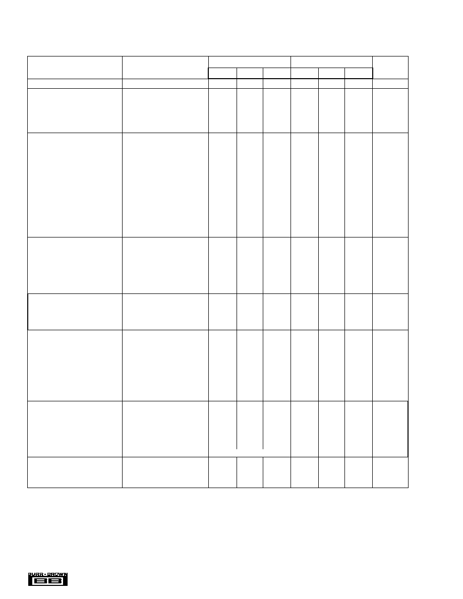
SPECIFICATIONS
All specifications T
MIN
to T
MAX
, +V
A
= +V
D
= +5V, V
REF
= internal +2.5V and f
CLK
= 8MHz, f
SAMPLE
= 500kHz, unless otherwise noted.
The information provided herein is believed to be reliable; however, BURR-BROWN assumes no responsibility for inaccuracies or omissions. BURR-BROWN assumes
no responsibility for the use of this information, and all use of such information shall be entirely at the user's own risk. Prices and specifications are subject to change
without notice. No patent rights or licenses to any of the circuits described herein are implied or granted to any third party. BURR-BROWN does not authorize or warrant
any BURR-BROWN product for use in life support devices and/or systems.
ADS7864Y
ADS7864YB
PARAMETER
CONDITIONS
MIN
TYP
MAX
MIN
TYP
MAX
UNITS
RESOLUTION
12
T
Bits
ANALOG INPUT
Input Voltage Range-Bipolar
V
CENTER
= +2.5V
≠V
REF
+V
REF
T
T
V
Absolute Input Range
+IN
≠0.3
+V
A
+ 0.3
V
≠IN
≠0.3
+V
A
+ 0.3
V
Input Capacitance
15
T
pF
Input Leakage Current
CLK = GND
±
1
T
µ
A
SYSTEM PERFORMANCE
No Missing Codes
12
T
Bits
Integral Linearity
±
0.75
±
2
±
0.5
±
1
LSB
Integral Linearity Match
0.5
T
LSB
Differential Linearity
≠0.9
±
0.6
T
±
0.4
LSB
Bipolar Offset Error
Referenced to REF
IN
±
0.75
±
4
±
0.5
±
3
LSB
Bipolar Offset Error Match
3
T
LSB
Positive Gain Error
Referenced to REF
IN
±
0.15
±
0.75
±
0.1
±
0.5
% of FSR
Positive Gain Error Match
3
T
LSB
Negative Gain Error
Referenced to REF
IN
±
0.15
±
0.75
±
0.1
±
0.5
% of FSR
Negative Gain Error Match
3
T
LSB
Common-Mode Rejection Ratio
At DC
84
T
dB
V
IN
=
±
1.25Vp-p at 50kHz
80
T
dB
Noise
120
T
µ
Vrms
Power Supply Rejection Ratio
0.3
2
T
T
LSB
SAMPLING DYNAMICS
Conversion Time per A/D
1.75
T
µ
s
Acquisition Time
0.25
T
µ
s
Throughput Rate
500
T
kHz
Aperture Delay
3.5
T
ns
Aperture Delay Matching
100
T
ps
Aperture Jitter
50
T
ps
Small-Signal Bandwidth
40
T
MHz
DYNAMIC CHARACTERISTICS
Total Harmonic Distortion
V
IN
=
±
2.5Vp-p at 100kHz
≠75
T
dB
SINAD
V
IN
=
±
2.5Vp-p at 100kHz
71
T
dB
Spurious Free Dynamic Range
V
IN
=
±
2.5Vp-p at 100kHz
78
T
dB
Channel-to-Channel Isolation
V
IN
=
±
2.5Vp-p at 50kHz
≠76
T
dB
VOLTAGE REFERENCE
Internal Reference Voltage
2.475
2.5
2.525
T
T
T
V
Internal Drift
10
T
ppm/
∞
C
Internal Noise
50
T
µ
Vp-p
Internal Source Current
2
T
mA
Internal Load Rejection
0.005
T
mV/
µ
A
Internal PSRR
80
T
dB
External Reference Voltage Range
1.2
2.5
2.6
T
T
T
V
Input Current
100
T
µ
A
Input Capacitance
5
T
pF
DIGITAL INPUT/OUTPUT
Logic Family
CMOS
T
Logic Levels: V
IH
I
IH
= +5
µ
A
3.0
+V
D
+ 0.3
T
T
V
V
IL
I
IL
= +5
µ
A
≠0.3
0.8
T
T
V
V
OH
I
OH
= ≠500
µ
A
3.5
T
V
V
OL
I
OL
= ≠500
µ
A
0.4
T
V
External Clock
0.2
8
T
T
MHz
Data Format
Binary Two's Complement
T
POWER SUPPLY REQUIREMENTS
Power Supply Voltage, +V
A
, +V
D
4.75
5
5.25
T
T
T
V
Quiescent Current, +V
A
, +V
D
10
T
mA
Power Dissipation
50
T
mW
T
Specifications same as ADS7864Y.

3
ADS7864
Æ
MINIMUM
RELATIVE
MAXIMUM
SPECIFICATION
PACKAGE
ACCURACY
GAIN ERROR
TEMPERATURE
DRAWING
ORDERING
TRANSPORT
PRODUCT
(LSB)
(%)
RANGE
PACKAGE
NUMBER
NUMBER
(1)
MEDIA
ADS7864Y
±
2
±
0.75
≠40
∞
C to +85
∞
C
TQFP-48
355
ADS7864Y/250
Tape and Reel
"
"
"
"
"
"
ADS7864Y/2K
Tape and Reel
ADS7864YB
±
1
±
0.5
≠40
∞
C to +85
∞
C
TQFP-48
355
ADS7864YB/250
Tape and Reel
"
"
"
"
"
"
ADS7864YB/2K
Tape and Reel
NOTES: (1) Models with a slash (/) are available only in Tape and Reel in the quantities indicated (e.g., /2K indicates 2000 devices per reel). Ordering 2000 pieces
of "ADS7864Y/2K" will get a single 2000-piece Tape and Reel.
PACKAGE/ORDERING INFORMATION
BASIC OPERATION
ABSOLUTE MAXIMUM RATINGS
Analog Inputs to AGND: Any Channel Input ........ ≠0.3V to (+V
D
+ 0.3V)
REF
IN
............................. ≠0.3V to (+V
D
+ 0.3V)
Digital Inputs to DGND .......................................... ≠0.3V to (+V
D
+ 0.3V)
Ground Voltage Differences: AGND, DGND ...................................
±
0.3V
+V
D
to AGND ......................... ≠0.3V to +6V
Power Dissipation .......................................................................... 325mW
Maximum Junction Temperature ................................................... +150
∞
C
Operating Temperature Range ........................................ ≠40
∞
C to +85
∞
C
Storage Temperature Range ......................................... ≠65
∞
C to +150
∞
C
Lead Temperature (soldering, 10s) ............................................... +300
∞
C
ELECTROSTATIC
DISCHARGE SENSITIVITY
This integrated circuit can be damaged by ESD. Burr-Brown
recommends that all integrated circuits be handled with
appropriate precautions. Failure to observe proper handling
and installation procedures can cause damage.
ESD damage can range from subtle performance degradation
to complete device failure. Precision integrated circuits may
be more susceptible to damage because very small parametric
changes could cause the device not to meet its published
specifications.
+V
A
AGND
DB15
DB14
DB13
DB12
DB11
DB10
DB9
DB8
DB7
DB6
1
2
3
4
5
6
7
8
9
10
11
12
36
35
34
33
32
31
30
29
28
27
26
25
+V
A
AGND
REFIN
REFOUT
RESET
A0
A1
A2
BYTE
HOLDA
HOLDB
HOLDC
DB5
DB4
DB3
DB2
DB1
DB0
BUSY
DGND
+V
D
CLOCK
RD
CS
Clock Input
Read Input
Chip Select
BUSY Output
13
14
15
16
17
18
19
20
21
22
23
24
CH A0+
CH A0≠
CH B0+
CH B0≠
CH C0+
CH C0≠
CH C1≠
CH C1+
CH B1≠
CH B1+
CH A1≠
CH A1+
48
47
46
45
44
ADS7864Y
43
42
41
40
39
38
37
0.1
µ
F
0.1
µ
F
DGND
Data Ouput
AGND
10
µ
F
+
10
µ
F
Address Select
Global Reset
+5V
Analog Power
Supply
+5V
Digital Power Supply
+
0.1
µ
F
10
µ
F
+5V
Analog Power
Supply
+
Sample and Hold
Inputs

4
ADS7864
Æ
PIN
NAME
DESCRIPTION
1
+V
A
Analog Power Supply. Normally +5V.
2
AGND
Analog Ground
3
DB15
Data Valid Output: "1" for data valid; "0" for invalid
data.
4
DB14
Channel Address Output Pin (see channel truth
table)
5
DB13
Channel Address Output Pin (see channel truth
table)
6
DB12
Channel Address Output Pin (see channel truth
table)
7
DB11
Data Bit 11 - MSB
8
DB10
Data Bit 10
9
DB9
Data Bit 9
10
DB8
Data Bit 8
11
DB7
Data Bit 7
12
DB6
Data Bit 6
13
DB5
Data Bit 5
14
DB4
Data Bit 4
15
DB3
Data Bit 3
16
DB2
Data Bit 2
17
DB1
Data Bit 1
18
DB0
Data Bit 0 - LSB
19
BUSY
Low when a conversion is in progress.
20
DGND
Digital Ground
21
+V
D
Digital Power Supply, +5VDC
22
CLOCK
An external clock must be applied to the CLOCK
input.
23
RD
RD Input. Enables the parallel output when used in
conjunction with chip select.
24
CS
Chip Select
PIN CONFIGURATION
Top View
PIN DESCRIPTIONS
+V
A
AGND
DB15
DB14
DB13
DB12
DB11
DB10
DB9
DB8
DB7
DB6
1
2
3
4
5
6
7
8
9
10
11
12
36
35
34
33
32
31
30
29
28
27
26
25
+V
A
AGND
REFIN
REFOUT
RESET
A0
A1
A2
BYTE
HOLDA
HOLDB
HOLDC
DB5
DB4
DB3
DB2
DB1
DB0
BUSY
DGND
+V
D
CLOCK
RD
CS
13
14
15
16
17
18
19
20
21
22
23
24
CH A0+
CH A0≠
CH B0+
CH B0≠
CH C0+
CH C0≠
CH C1≠
CH C1+
CH B1≠
CH B1+
CH A1≠
CH A1+
48
47
46
45
44
ADS7864
43
42
41
40
39
38
37
25
HOLDC
Places Channels C0 and C1 in hold mode.
26
HOLDB
Places Channels B0 and B1 in hold mode.
27
HOLDA
Places Channels A0 and A1 in hold mode.
28
BYTE
2 x 8 Output Capability. Active HIGH
29
A2
A2 Address/Mode Select Pin (see Address/Mode Truth
table).
30
A1
A1 Address/Mode Select Pin (see Address/Mode Truth
Table).
31
A0
A0 Address/Mode Select Pin (see Address/Mode Truth
Table).
32
RESET
Reset Pin
33
REFOUT
Reference Out
34
REFIN
Reference In
35
AGND
Analog Ground
36
+V
A
Analog Power Supply. Normally +5V.
37
CH A1+
Noninverting Input Channel A1
38
CH A1≠
Inverting Input Channel A1
39
CH B1+
Noninverting Input Channel B1
40
CH B1≠
Inverting Input Channel B1
41
CH C1+
Noninverting Input Channel C1
42
CH C1≠
Inverting Input Channel C1
43
CH C0≠
Inverting Input Channel C0
44
CH C0+
Noninverting Input Channel C0
45
CH B0≠
Inverting Input Channel B0
46
CH B0+
Noninverting Input Channel B0
47
CH A0≠
Inverting Input Channel A0
48
CH A0+
Noninverting Input Channel A0
PIN
NAME
DESCRIPTION

5
ADS7864
Æ
TYPICAL PERFORMANCE CURVES
At T
A
= +25
∞
C, +V
A
= +V
D
= +5V, V
REF
= internal +2.5V and f
CLK
= 8MHz, f
SAMPLE
= 500kHz, unless otherwise noted.
FREQUENCY SPECTRUM
(4096 Point FFT; f
IN
= 99.9kHz, ≠0.2dB)
Frequency (kHz)
0
≠20
≠40
≠60
≠80
≠100
≠120
Amplitude (dB)
0
62.5
125
250
187.5
FREQUENCY SPECTRUM
(4096 Point FFT; f
IN
= 199.9kHz, ≠0.2dB)
Frequency (kHz)
0
≠20
≠40
≠60
≠80
≠100
≠120
Amplitude (dB)
0
62.5
125
250
187.5
SIGNAL-TO-NOISE RATIO AND
SIGNAL-TO-(NOISE+DISTORTION)
vs INPUT FREQUENCY
10k
100k
1k
1M
Input Frequency (Hz)
SNR and SINAD (dB)
75
70
65
60
55
50
SINAD
SNR
SNR
CHANGE IN SIGNAL-TO-NOISE RATIO
AND SIGNAL-TO-(NOISE+DISTORTION)
vs TEMPERATURE
1.0
0.6
0.2
≠0.2
≠0.6
≠1.0
Delta from +25
∞
C (dB)
SINAD
Temperature (
∞
C)
≠20
≠40
0
20
40
60
80
CHANGE IN SPURIOUS FREE DYNAMIC RANGE
AND TOTAL HARMONIC DISTORTION
vs TEMPERATURE
Temperature (
∞
C)
1.0
0.5
0.0
≠0.5
≠1.0
THD and SFDR Delta from +25
∞
C (dB)
≠20
≠40
0
20
40
60
80
THD
SFDR
POSITIVE GAIN MATCH vs TEMPERATURE
(Maximum Deviation for All Six Channels)
Temperature (
∞
C)
Change in Positive Gain Match (LSB)
1.80
1.70
1.60
1.50
1.40
1.30
1.20
≠20
≠40
0
20
40
60
80