 | –≠–ª–µ–∫—Ç—Ä–æ–Ω–Ω—ã–π –∫–æ–º–ø–æ–Ω–µ–Ω—Ç: ADS804 | –°–∫–∞—á–∞—Ç—å:  PDF PDF  ZIP ZIP |
ADS804
Æ
12-Bit, 10MHz Sampling
ANALOG-TO-DIGITAL CONVERTER
©
1997 Burr-Brown Corporation
PDS-1381C
Printed in U.S.A. October, 1998
TM
International Airport Industrial Park ∑ Mailing Address: PO Box 11400, Tucson, AZ 85734 ∑ Street Address: 6730 S. Tucson Blvd., Tucson, AZ 85706 ∑ Tel: (520) 746-1111 ∑ Twx: 910-952-1111
Internet: http://www.burr-brown.com/ ∑ FAXLine: (800) 548-6133 (US/Canada Only) ∑ Cable: BBRCORP ∑ Telex: 066-6491 ∑ FAX: (520) 889-1510 ∑ Immediate Product Info: (800) 548-6132
ADS804E
ADS804U
DEMO BOARD
AVAILABLE
FEATURES
q
HIGH SFDR: 80dB at NYQUIST
q
HIGH SNR: 69dB
q
LOW POWER: 180mW
q
SMALL 28-LEAD SSOP AND SOIC PACKAGES
q
LOW DLE:
±
0.3LSB
q
FLEXIBLE INPUT RANGE
q
OVERRANGE INDICATOR
APPLICATIONS
q
IF AND BASEBAND DIGITIZATION
q
CCD IMAGING
q
SCANNERS
q
TEST INSTRUMENTATION
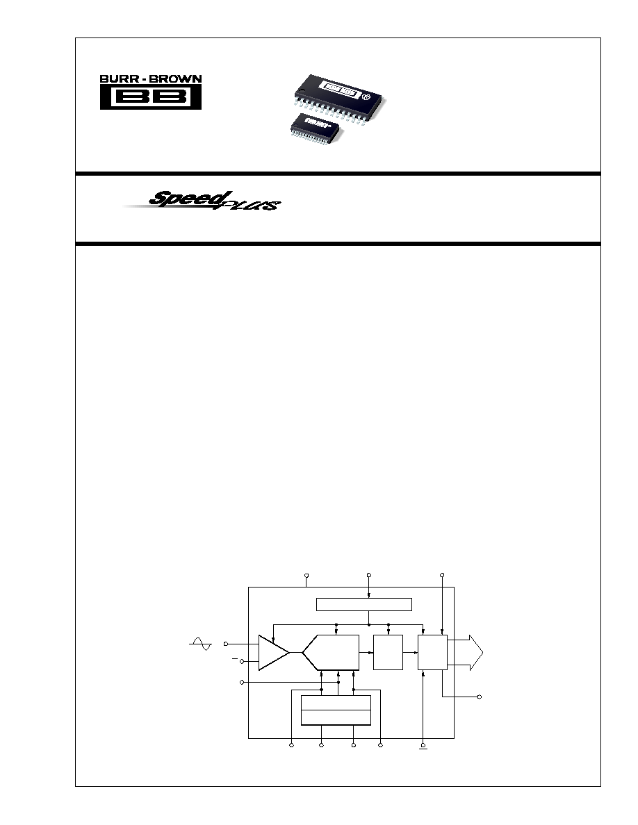
DESCRIPTION
The ADS804 is a high-speed, high dynamic range, 12-bit pipelined
analog-to-digital converter. This converter includes a high-band-
width track/hold that gives excellent spurious performance up to
and beyond the Nyquist rate. This high-bandwidth, linear track/hold
minimizes harmonics and has low jitter, leading to excellent SNR
performance. The ADS804 is also pin-compatible with the 5MHz
ADS803 and the 20MHz ADS805.
The ADS804 provides an internal reference and can be programmed
for a 2Vp-p input range for the best spurious performance and ease
of driving. Alternatively, the 5Vp-p input range can be used for the
lowest input referred noise of 0.09 LSBs rms giving superior
imaging performance. There is also a capability to set the input
range in between the 2Vp-p and 5Vp-p input ranges or to use
external reference. The ADS804 also provides an overrange indica-
tor flag to indicate an input range that exceeds the full-scale input
range of the converter. This flag can be used to reduce the gain of
the front end gain-ranging circuitry.
The ADS804 employs digital error correction techniques to provide
excellent differential linearity for demanding imaging applications.
Its low distortion and high SNR give the extra margin needed for
communications, medical imaging, video and test instrumentation
applications. The ADS804 is available in 28-Lead SSOP and SOIC
packages.
12-Bit
Pipelined
A/D Core
Reference and
Mode Select
Reference Ladder
and Driver
Timing Circuitry
Error
Correction
Logic
3-State
Outputs
T/H
D0
D11
∑
∑
∑
CLK
+V
S
ADS804
VDRV
OE
SEL
REFB
V
REF
REFT
IN
V
IN
IN
(Opt.)
CM
OVR
2
Æ
ADS804
SPECIFICATIONS
At T
A
= full specified temperature range, V
S
= +5V, specified single-ended input range = 1.5V to 3.5V, sampling rate = 10MHz, unless otherwise specified.
CMOS Compatible
Rising Edge of Convert Clock
CMOS Compatible
Rising Edge of Convert Clock
CMOS/TTL Compatible
Straight Offset Binary
CMOS/TTL Compatible
Straight Offset Binary
ADS804U
ADS804E
PARAMETER
CONDITIONS
MIN
TYP
MAX
MIN
TYP
MAX
UNITS
RESOLUTION
12
T
(1)
Bits
SPECIFIED TEMPERATURE RANGE
≠40 to +85
≠40 to +85
∞
C
CONVERSION CHARACTERISTICS
Sample Rate
10k
10M
T
T
Samples/s
Data Latency
6
T
Clk Cycles
ANALOG INPUT
Single-Ended Input Range
2Vp-p
1.5
3.5
T
T
V
Single-Ended Input Range (Optional)
5Vp-p
0
5
T
T
V
Common-Mode Voltage
+2.5
T
V
Input Impedance
1.25 || 16
T
M
|| pF
Track-Mode Input Bandwidth
≠3dBFS Input
270
T
MHz
DYNAMIC CHARACTERISTICS
Differential Linearity Error (Largest Code Error)
f = 500kHz
±
0.3
±
0.75
T
T
LSB
No Missing Codes
Guaranteed
Guaranteed
Spurious Free Dynamic Range
(2)
f = 4.8MHz
73
80
T
T
dBFS
Two-Tone Intermodulation Distortion
(4)
f = 3.5MHz and 4.0MHz (≠7dBFS each tone)
76
T
dBc
Signal-to-Noise Ratio (SNR)
f = 4.8MHz
66.5
69
T
T
dBFS
Signal-to-(Noise + Distortion) (SINAD)
f = 4.8MHz
65
68
T
T
dBFS
Effective Number of Bits at 4.8MHz
(5)
11
T
Bits
Input Referred Noise
0V to 5V Input
0.09
T
LSBs rms
1.5V to 3.5V Input
0.23
T
LSBs rms
Integral Nonlinearity Error
f = 500kHz
±
1
±
2
T
T
LSB
Aperture Delay Time
1
T
ns
Aperture Jitter
4
T
ps rms
Overvoltage Recovery Time
1.5 x FS Input
2
T
ns
Full-Scale Step Acquisition Time
30
T
ns
DIGITAL INPUTS
Logic Family
Convert Command
Start Conversion
High Level Input Current (V
IN
= 5V)
(6)
100
T
µ
A
Low Level Input Current (V
IN
= 0V)
10
T
µ
A
High Level Input Voltage
+3.5
T
V
Low Level Input Voltage
+1.0
T
V
Input Capacitance
5
T
pF
DIGITAL OUTPUTS
Logic Family
Convert Command
Output Voltages, V
DRV
= +5V
Low-Level
I
OL
= 50
µ
A
+0.1
T
V
High-Level
I
OH
= 50
µ
A
+4.6
T
V
Low-Level
I
OL
= 1.6mA
+0.4
T
V
High-Level
I
OH
= 0.5mA
+2.4
T
V
Output Voltages, V
DRV
= +3V
Low-Level
I
OL
= 50
µ
A
+0.1
T
V
High-Level
I
OH
= 50
µ
A
+2.5
T
V
3-State Enable Time
OE = L
20
40
T
T
ns
3-State Enable Time
OE = H
2
10
T
T
ns
Output Capacitance
5
T
pF
ACCURACY (5Vp-p Input Range)
Zero Error (Referred to ≠FS)
At 25
∞
C
0.2
±
1.5
T
T
%FS
Zero Error Drift
±
5
T
ppm/
∞
C
Gain Error
(7)
At 25
∞
C
±
2.0
T
%FS
Gain Error Drift
(7)
±
15
T
ppm/
∞
C
Gain Error
(8)
At 25
∞
C
±
1.5
T
%FS
Gain Error Drift
(8)
±
15
T
ppm/
∞
C
Power Supply Rejection of Gain
V
S
=
±
5%
60
82
T
T
dB
Reference Input Resistance
1.6
T
k
Internal Voltage Reference Tolerance (V
REF
= 2.5V)
At 25
∞
C
±
35
T
mV
Internal Voltage Reference Tolerance (V
REF
= 1.0V)
At 25
∞
C
±
14
T
mV
3
Æ
ADS804
POWER SUPPLY REQUIREMENTS
Supply Voltage: +V
S
+4.7
+5.0
+5.3
T
T
T
V
Supply Current: +I
S
36
40
T
T
mA
Power Dissipation
180
200
T
T
mW
Thermal Resistance,
JA
28-Lead SOIC
75
∞
C/W
28-Lead SSOP
50
∞
C/W
NOTES: (1) An asterisk (
T
) indicates same specifications as the ADS804U. (2) Spurious Free Dynamic Range difference in dB between the rms input amplitude
to the peak spar level in the output frequency spectrum. (3) dBFS means dB relative to full scale. (4) Two-tone intermodulation distortion is referred to the largest
fundamental tone. This number will be 6dB higher if it is referred to the magnitude of the two-tone fundamental envelope. (5) Effective number of bits (ENOB) is
defined by (SINAD ≠ 1.76)/6.02. (6) Internal 50k
pull-down resistor. (7) Includes internal reference. (8) Excludes internal reference.
The information provided herein is believed to be reliable; however, BURR-BROWN assumes no responsibility for inaccuracies or omissions. BURR-BROWN
assumes no responsibility for the use of this information, and all use of such information shall be entirely at the user's own risk. Prices and specifications are subject
to change without notice. No patent rights or licenses to any of the circuits described herein are implied or granted to any third party. BURR-BROWN does not
authorize or warrant any BURR-BROWN product for use in life support devices and/or systems.
SPECIFICATIONS
(CONT)
At T
A
= full specified temperature range, V
S
= +5V, specified single-ended input range = 1.5V to 3.5V, sampling rate = 10MHz, unless otherwise specified.
ADS804U
ADS804E
PARAMETER
CONDITIONS
MIN
TYP
MAX
MIN
TYP
MAX
UNITS
ELECTROSTATIC
DISCHARGE SENSITIVITY
This integrated circuit can be damaged by ESD. Burr-Brown
recommends that all integrated circuits be handled with
appropriate precautions. Failure to observe proper handling
and installation procedures can cause damage.
ESD damage can range from subtle performance degradation
to complete device failure. Precision integrated circuits may
be more susceptible to damage because very small parametric
changes could cause the device not to meet its published
specifications.
+V
S
, VDRV ........................................................................................... +6V
Analog Input ........................................................... (≠0.3V) to (+V
S
+0.3V)
Logic Input ............................................................. (≠0.3V) to (+V
S
+0.3V)
Case Temperature ......................................................................... +100
∞
C
Junction Temperature .................................................................... +150
∞
C
Storage Temperature ..................................................................... +150
∞
C
ABSOLUTE MAXIMUM RATINGS
DEMO BOARD ORDERING INFORMATION
PRODUCT
DEMO BOARD
ADS804U
DEM-ADS80xU
PACKAGE
SPECIFIED
DRAWING
TEMPERATURE
PACKAGE
ORDERING
TRANSPORT
PRODUCT
PACKAGE
NUMBER
(1)
RANGE
MARKING
NUMBER
MEDIA
ADS804U
SO-28 Surface Mount
217
≠40
∞
C to +85
∞
C
ADS804U
ADS804U
Rails
ADS804E
SSOP-28 Surface Mount
324
≠40
∞
C to +85
∞
C
ADS804E
ADS804E
Rails
"
"
"
"
"
ADS804E/1K
Tape and Reel
NOTES: (1) For detailed drawing and dimension table, please see end of data sheet, or Appendix C of Burr-Brown IC Data Book. For detailed Tape and Reel
mechanical information refer to Appendix B of Burr-Brown IC Data Book.
PACKAGE/ORDERING INFORMATION
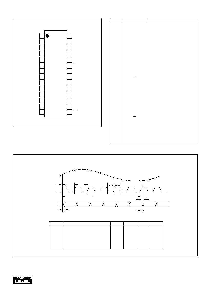
4
Æ
ADS804
6 Clock Cycles
Data Invalid
t
D
t
L
t
H
t
CONV
N≠6
N≠5
N≠4
N≠3
N≠2
N-1
N
N+1
Data Out
Clock
Analog In
N
t
2
N+1
N+2
N+3
N+4
N+5
N+6
N+7
t
1
PIN
DESIGNATOR
DESCRIPTION
1
OVR
Over Range Indicator (See Application
Section)
2
B1
Data Bit 1(D11) (MSB)
3
B2
Data Bit 2 (D10)
4
B3
Data Bit 3 (D9)
5
B4
Data Bit 4 (D8)
6
B5
Data Bit 5 (D7)
7
B6
Data Bit 6 (D6)
8
B7
Data Bit 7 (D5)
9
B8
Data Bit 8 (D4)
10
B9
Data Bit 9 (D3)
11
B10
Data Bit 10 (D2)
12
B11
Data Bit 11 (D1)
13
B12
Data Bit 12 (D0) (LSB)
14
CLK
Convert Clock Input
15
OE
Output Enable. H = High Impedance State.
L = Low or floating, normal operation
(Internal pull-down resistor).
16
+V
S
+5V Supply
17
GND
Ground
18
SEL
Input Range Select (See Application
Section)
19
V
REF
Reference Voltage Select (I/O)
20
REFB
Bottom Reference
21
CM
Common-Mode Voltage
22
REFT
Top Reference
23
IN
Analog Input (≠)
24
GND
Ground
25
IN
Analog Input (+)
26
GND
Ground
27
+V
S
+5V Supply
28
VDRV
Output Driver Voltage (See Application
Section).
PIN CONFIGURATION
PIN DESCRIPTIONS
Top View
SOIC/SSOP
TIMING DIAGRAM
SYMBOL
DESCRIPTION
MIN
TYP
MAX
UNITS
t
CONV
Convert Clock Period
100
100
µ
s
ns
t
L
Clock Pulse Low
48
49
ns
t
H
Clock Pulse High
48
49
ns
t
D
Aperture Delay
2
ns
t
1
Data Hold Time, C
L
= 0pF
3.9
ns
t
2
New Data Delay Time, C
L
= 15pF max
12
ns
OVR
B1
B2
B3
B4
B5
B6
B7
B8
B9
B10
B11
B12
CLK
VDRV
+V
S
GND
IN
GND
IN
REFT
CM
REFB
V
REF
SEL
GND
+V
S
OE
1
2
3
4
5
6
7
8
9
10
11
12
13
14
28
27
26
25
24
23
22
21
20
19
18
17
16
15
ADS804
5
Æ
ADS804
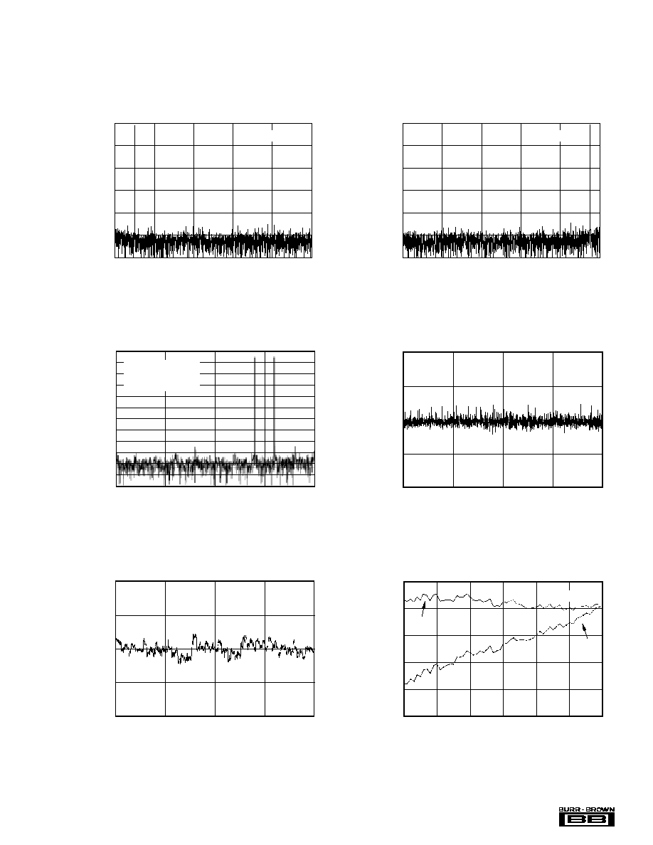
SPECTRAL PERFORMANCE
Frequency (MHz)
Amplitude (dB)
0
1.0
2.0
3.0
4.0
5.0
0
≠20
≠40
≠60
≠80
≠100
≠120
f
IN
= 4.8MHz
SPECTRAL PERFORMANCE
Frequency (MHz)
Amplitude (dB)
0
1.0
2.0
3.0
4.0
5.0
0
≠20
≠40
≠60
≠80
≠100
≠120
f
IN
= 500kHz
INTEGRAL LINEARITY ERROR
Output Code
ILE (LSB)
0
1024
2048
3072
4096
4.0
2.0
0
≠2.0
≠4.0
f
IN
= 500kHz
TYPICAL PERFORMANCE CURVES
At T
A
= full specified temperature range, V
S
= +5V, specified single-ended input range = 1.5V to 3.5V, sampling rate = 10MHz, unless otherwise specified.
DIFFERENTIAL LINEARITY ERROR
Output Code
DLE (LSB)
0
1024
2048
3072
4096
1.0
0.5
0
≠0.5
≠1.0
f
IN
= 4.8MHz
100
80
60
40
20
0
SWEPT POWER SFDR
SFDR (dBFS, dBc)
≠60
≠50
≠40
≠30
≠20
≠10
0
Input Amplitude (dBFS)
f
IN
= 4.8MHz
dBFS
dBc
0
≠20
≠40
≠60
≠80
≠100
≠120
TWO-TONE INTERMODULATION
Frequency (MHz)
Magnitude (dBFSR)
0
1.25
2.5
3.75
5.0
f
1
= 3.5MHz at ≠7dB
f
2
= 4MHz at ≠7dB
IMD (3) = ≠76dBc