 | ÐлекÑÑоннÑй компоненÑ: ADS8323 | СкаÑаÑÑ:  PDF PDF  ZIP ZIP |
Äîêóìåíòàöèÿ è îïèñàíèÿ www.docs.chipfind.ru
ADS8323
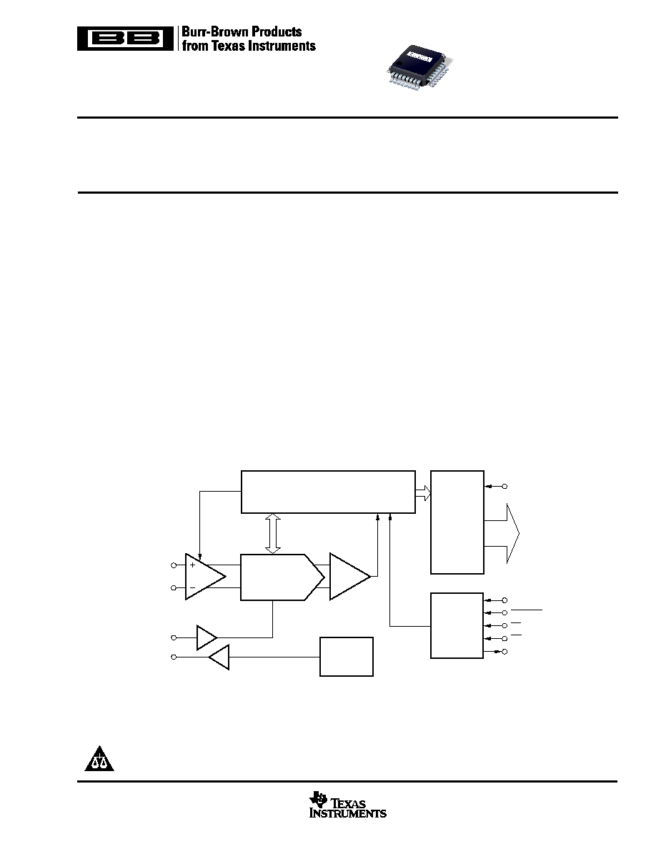
DESCRIPTION
The ADS8323 is a 16-bit, 500kSPS Analog-to-Digital Con-
verter (ADC) with an internal 2.5V reference. The device
includes a 16-bit capacitor-based SAR ADC with inherent
sample-and-hold. The ADS8323 offers a full 16-bit interface,
or an 8-bit option where data is read using two read cycles.
The ADS8323 is available in a TQFP-32 package and is
specified over the industrial 40
°
C to +85
°
C temperature
range.
FEATURES
q
HIGH-SPEED PARALLEL INTERFACE
q
500kSPS SAMPLING RATE
q
LOW POWER: 85mW at 500kSPS
q
BIPOLAR INPUT RANGE
q
TQFP-32 PACKAGE
APPLICATIONS
q
HIGH-SPEED DATA AQUISITION
q
OPTICAL POWER MONITORING
q
MOTOR CONTROL
q
ATE
SAR
Output Latches
and
Three State
Drivers
Comparator
ADS8323
S/H Amp
BYTE
Parallel
Data
Output
+IN
IN
CDAC
REF
IN
Conversion
and Control
Logic
Internal
+2.5V Ref
CONVST
CLOCK
CS
RD
BUSY
REF
OUT
ADS8
323
®
16-Bit, 500kSPS,
microPower Sampling
ANALOG-TO-DIGITAL CONVERTER
SBAS224B DECEMBER 2001 REVISED MAY 2002
www.ti.com
PRODUCTION DATA information is current as of publication date.
Products conform to specifications per the terms of Texas Instruments
standard warranty. Production processing does not necessarily include
testing of all parameters.
Copyright © 2001, Texas Instruments Incorporated
Please be aware that an important notice concerning availability, standard warranty, and use in critical applications of
Texas Instruments semiconductor products and disclaimers thereto appears at the end of this data sheet.
ADS8323
2
SBAS224B
www.ti.com
MAXIMUM
NO
INTEGRAL
MISSING
SPECIFICATION
LINEARITY
CODES
PACKAGE
TEMPERATURE
ORDERING
TRANSPORT
PRODUCT
ERROR (LSB)
ERROR (LSB)
PACKAGE-LEAD
DESIGNATOR
(1)
RANGE
NUMBER
MEDIA, QUANTITY
ADS8323Y
±
8
14
TQFP-32
PBS
40
°
C to 85
°
C
ADS8323Y/250
Tape and Reel, 250
"
"
"
"
"
"
ADS8323Y/2K
Tape and Reel, 2000
ADS8323YB
±
6
15
TQFP-32
PBS
40
°
C to 85
°
C
ADS8323YB/250
Tape and Reel, 250
"
"
"
"
"
"
ADS8323YB/2K
Tape and Reel, 2000
NOTE: (1) For the most current specifications and package information, refer to our web site at www.ti.com.
PACKAGE/ORDERING INFORMATION
ABSOLUTE MAXIMUM RATINGS
Absolute Maximum Ratings over operating free-air temperature (unless
otherwise noted)
(1)
Supply Voltage, DGND to DV
DD ..............................................................
0.3V to 6V
Supply Voltage, AGND to AV
DD ...............................................................
0.3V to 6V
Analog Input Voltage Range ..................... AGND - 0.3V to AV
DD
+ 0.3V
Reference Input Voltage ........................... AGND - 0.3V to AV
DD
+ 0.3V
Digital Input Voltage Range ...................... DGND - 0.3V to DV
DD
+ 0.3V
Ground Voltage Differences, AGND to DGND ................................
±
0.3V
Voltage Differences, DV
DD
to AGND ..................................... 0.3V to 6V
Power Dissipation .......................................................................... 850mW
Operating Virtual Junction Temperature Range, T
J
........ 40
°
C to 150
°
C
Operating Free-Air Temperature Range, T
A
...................... 40
°
C to 85
°
C
Storage Temperature Range, T
STG
.................................. 65
°
C to 150
°
C
Lead Temperature 1.6mm (1/16 inch) from Case for 10sec ..................... 260
°
C
ELECTROSTATIC
DISCHARGE SENSITIVITY
This integrated circuit can be damaged by ESD. Texas
Instruments recommends that all integrated circuits be handled
with appropriate precautions. Failure to observe proper han-
dling and installation procedures can cause damage.
ESD damage can range from subtle performance degrada-
tion to complete device failure. Precision integrated circuits
may be more susceptible to damage because very small
parametric changes could cause the device not to meet its
published specifications.
NOTE: (1) Stresses beyond those listed under "absolute maximum ratings" may
cause permanent damage to the device. These are stress ratings only, and
functional operation of the device at these or any other conditions beyond those
indicated under "recommended operating conditions" is not implied. Exposure
to absolute-maximum-rated conditions of extended periods may affect device
reliability.
POWER SUPPLY
MIN
TYP
MAX
UNIT
Supply Voltage
AV
DD
(1)
4.75
5.0
5.25
V
DV
DD
(1)
4.75
5.0
5.25
V
ANALOG/REFERENCE INPUTS
Differential analog input voltage
REF
IN
+REF
IN
V
(IN+ to IN)
External Reference Voltage
1.5
2.5
2.55
V
NOTE: (1) The voltage difference between AV
DD
and DV
DD
terminals cannot
exceed 0.3V to maintain performance specifications.
DERATING
T
A
25
°
C
FACTOR
T
A
= 70
°
C
T
A
= 85
°
C
POWER
ABOVE
POWER
POWER
PACKAGE
RATING
T
A
= 25
°
C
(1)
RATING
RATING
TQFP-32
1636mW
13.09mW/
°
C
1047mW
850mW
NOTE: (1) This is the inverse of the traditional junction-to-ambient thermal
resistance (R
JA
). Thermal resistances are not production tested and are for
informational purposes only.
RECOMMENDED OPERATING CONDITIONS
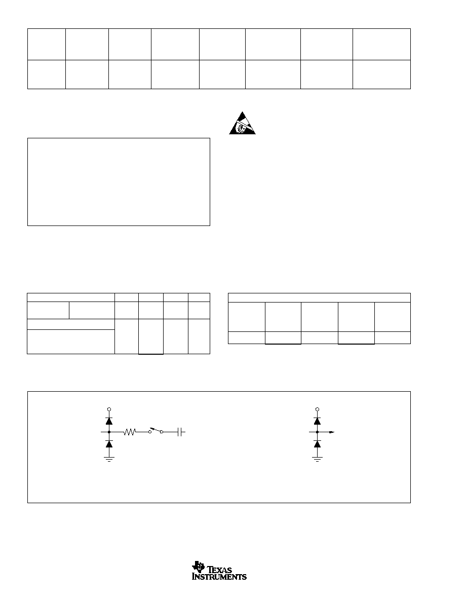
EQUIVALENT INPUT CIRCUIT
DISSIPATION RATING TABLE
R
ON
20
C
(SAMPLE)
20pF
DV
DD
D
IN
DGND
AV
DD
A
IN
AGND
Diode Turn-On Voltage: 0.35V
Equivalent Analog Input Circuit
Equivalent Digital Input Circuit
ADS8323
3
SBAS224B
www.ti.com
ELECTRICAL CHARACTERISTICS
At 40
°
C to +85
°
C, +DV
DD
= +AV
DD
= +5V, V
REF
= +2.5V, f
SAMPLE
= 500kSPS, and f
CLK
= 20 · f
SAMPLE
, unless otherwise specified.
ADS8323Y
ADS8323YB
PARAMETER
CONDITIONS
MIN
TYP
MAX
MIN
TYP
MAX
UNITS
RESOLUTION
16
Bits
ANALOG INPUT
Full-Scale Input Span
(1)
+IN (IN)
V
REF
+V
REF
V
Absolute Input Range
+IN
0.3
AV
DD
+ 0.3
V
IN
0.3
AV
DD
+ 0.3
V
Capacitance
25
pF
Leakage Current
±
1
nA
SYSTEM PERFORMANCE
No Missing Codes
14
15
Bits
Integral Linearity Error
±
4
±
8
±
3
±
6
LSB
(2)
Differential Linearity Error
±
3
±
1
LSB
Offset Error
±
1
±
2
±
0.5
±
1
mV
Gain Error
(3)
±
0.25
±
0.5
±
0.12
±
0.25
% of FSR
Common-Mode Rejection Ratio
At DC
70
dB
V
IN
= 1Vp-p at 1MHz
50
dB
Noise
60
µ
Vrms
Power-Supply Rejection
At FFFF
H
Output Code
±
3
LSB
SAMPLING DYNAMICS
Conversion Time
1.6
µ
s
Acquisition Time
0.4
µ
s
Throughput Rate
500
kSPS
Aperture Delay
10
ns
Aperture Jitter
30
ps
Small-Signal Bandwidth
20
MHz
Step Response
100
ns
Overvoltage Recovery
150
ns
DYNAMIC CHARACTERISTICS
Total Harmonic Distortion
(4)
V
IN
= 5Vp-p at 100kHz
90
93
dB
SINAD
V
IN
= 5Vp-p at 100kHz
81
83
dB
Spurious-Free Dynamic Range
V
IN
= 5Vp-p at 100kHz
94
96
dB
REFERENCE OUTPUT
Voltage
I
OUT
= 0
2.475
2.50
2.525
2.48
2.52
V
Source Current
Static Load
10
µ
A
Drift
I
OUT
= 0
25
ppm/
°
C
Line Regulation
4.75V
V
CC
5.25V
0.6
mV
REFERENCE INPUT
Range
1.5
2.55
V
DIGITAL INPUT/OUTPUT
Logic Family
CMOS
Logic Levels:
V
IH
I
IH
+5
µ
A
3.0
+DV
DD
V
V
IL
I
IL
5
µ
A
0.3
0.8
V
V
OH
I
OH
= 1.6mA
4.0
V
V
OL
I
OL
= +1.6mA
0.4
V
Data Format
Binary Two's Complement
POWER-SUPPLY REQUIREMENT
Power-Supply Voltage
+AV
DD
4.75
5
5.25
V
+DV
DD
4.75
5
5.25
V
Supply Current
f
SAMPLE
= 500kSPS
17
25
mA
Power Dissipation
f
SAMPLE
= 500kSPS
85
125
mW
TEMPERATURE RANGE
Specified Performance
40
+85
°
C
Specifications same as ADS8323Y.
NOTES: (1) Ideal input span; does not include gain or offset error. (2) LSB means Least Signifcant Bit, with V
REF
equal to +2.5V; 1LSB = 76
µ
V. (3) Measured relative
to an ideal, full-scale input (+In (In)) of 4.9999V. Thus, gain error includes the error of the internal voltage reference. (4) Calculated on the first nine harmonics
of the input frequency.
ADS8323
4
SBAS224B
www.ti.com
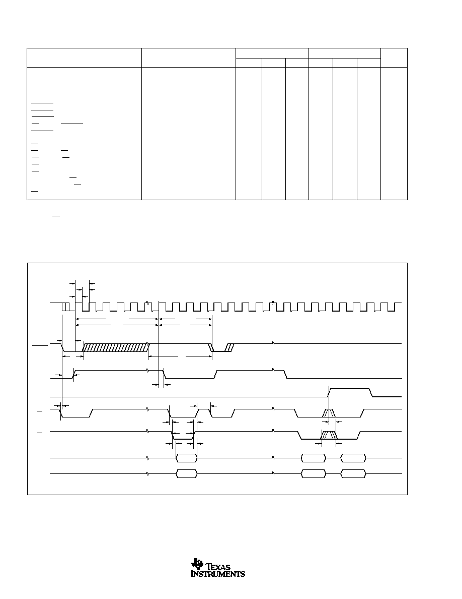
1
CLOCK
Acquisition
CONVST
BUSY
BYTE
CS
RD
DB15-D8
DB7-D0
2
3
4
5
17
18
19
20
3
4
1
2
17
18
19
20
t
C1
t
W1
t
D1
t
W3
t
W4
Acquisition
Conversion
t
ACQ
t
CONV
t
D2
t
D4
t
W5
t
D5
t
D6
t
D3
t
D7
t
W6
t
D8
Bits 15-8
Bits 15-8
FF
t
D9
t
W7
t
W2
Bits 7-0
Bits 7-0
Bits 15-8
ADS8323Y
ADS8323YB
PARAMETER
SYMBOL
MIN
TYP
MAX
MIN
TYP
MAX
UNITS
Conversion Time
t
CONV
1.6
µ
s
Acquisition Time
t
ACQ
0.4
µ
s
CLOCK Period
t
C1
100
ns
CLOCK HIGH Time
t
W1
40
ns
CLOCK LOW Time
t
W2
40
ns
CONVST LOW to CLOCK HIGH
t
D1
10
ns
CONVST LOW Time
t
W3
20
ns
CONVST LOW to BUSY HIGH
t
D2
25
ns
CS LOW to CONVST LOW
t
D3
0
ns
CONVST HIGH
t
W4
20
ns
CLOCK HIGH to BUSY LOW
t
D4
25
ns
CS HIGH
t
W5
0
ns
CS LOW to RD LOW
t
D5
0
ns
RD HIGH to CS HIGH
t
D6
0
ns
RD LOW Time
t
W6
50
ns
RD LOW to Data Valid
t
D7
40
ns
Data Hold from RD HIGH
t
D8
5
ns
BYTE Change to RD LOW
(3)
t
D9
0
ns
RD HIGH Time
t
W7
20
ns
NOTES: (1) All input signals are specified with rise and fall times of 5ns, t
R
= t
F
= 5ns (10% to 90% of DV
DD
), and timed from a voltage level of (V
IL
+ V
IH
) /2. (2)
See timing diagram, below. (3) BYTE is asynchronous; when BYTE is 0, bits 15 through 0 appear at DB15-DB0. When BYTE is 1, bits 15 through 8 appear on
DB7-DB0. RD may remain LOW between changes in BYTE.
TIMING CHARACTERISTICS
(1)(2)
All specifications typical at 40
°
C to +85
°
C, +DV
DD
= +5V.
TIMING DIAGRAM
ADS8323
5
SBAS224B
www.ti.com
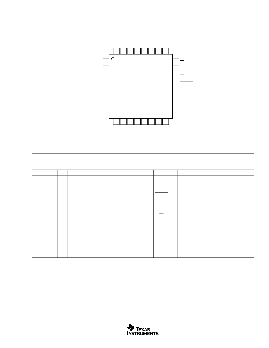
PIN CONFIGURATION
Top View
TQFP
DB15
DB14
DB13
DB12
DB11
DB10
DB9
DB8
1
2
3
4
5
6
7
8
24
23
22
21
20
19
18
17
CS
BYTE
RD
CONVST
CLOCK
DGND
+DV
DD
BUSY
DB7
DB6
DB5
DB4
DB3
DB2
DB1
DB0
9
10
11
12
13
14
15
16
REF
OUT
REF
IN
NC
NC
+AV
DD
AGND
+IN
IN
32
31
30
29
28
ADS8323
27
26
25
19
DGND
P
Digital Ground
20
CLOCK
DI
An external CMOS compatible clock can be applied
to the CLOCK input to synchronize the conversion
process to an external source.
21
CONVST
DI
Convert Start, Active LOW.
22
RD
DI
Synchronization pulse for the parallel output, Active
LOW.
23
BYTE
DI
Selects 8 most significant bits (LOW) or 8 least
significant bits (HIGH). Data valid on pins 9-16.
24
CS
DI
Chip Select, Active LOW.
25
IN
AI
Inverting Input Channel
26
+IN
AI
Noninverting Input Channel
27
AGND
P
Analog Ground
28
+AV
DD
P
Analog Power Supply, +5VDC.
29
NC
--
No Connect
30
NC
--
No Connect
31
REF
IN
AI
Reference Input. When using the internal 2.5V
reference tie this pin directly to REF
OUT
.
32
REF
OUT
AO
Reference Output
PIN
NAME
I/O
DESCRIPTION
1
DB15
DO
Data Bit 15 - MSB
2
DB14
DO
Data Bit 14
3
DB13
DO
Data Bit 13
4
DB12
DO
Data Bit 12
5
DB11
DO
Data Bit 11
6
DB10
DO
Data Bit 10
3
DB9
DO
Data Bit 9
8
DB8
DO
Data Bit 8
9
DB7
DO
Data Bit 7
10
DB6
DO
Data Bit 6
11
DB5
DO
Data Bit 5
12
DB4
DO
Data Bit 4
13
DB3
DO
Data Bit 3
14
DB2
DO
Data Bit 2
15
DB1
DO
Data Bit 1
16
DB0
DO
Data Bit 0 - LSB
17
BUSY
DO
HIGH when a conversion is in progress.
18
+DV
DD
P
Digital Power Supply, +5VDC.
PIN ASSIGNMENTS
PIN
NAME
I/O
DESCRIPTION
NOTE: AI is Analog Input, AO is Analog Output, DI is Digital Input, DO is Digital Output, and P is Power-Supply Connection.