 | –≠–ª–µ–∫—Ç—Ä–æ–Ω–Ω—ã–π –∫–æ–º–ø–æ–Ω–µ–Ω—Ç: ADS8328I | –°–∫–∞—á–∞—Ç—å:  PDF PDF  ZIP ZIP |
Burr Brown Products
from Texas Instruments
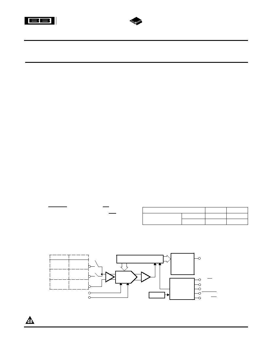
FEATURES
APPLICATIONS
DESCRIPTION
REF-
+IN
REF+
SDI
SCLK
SDO
CDAC
SAR
COMPARATOR
OUTPUT
LATCH
and
3-STATE
DRIVER
CONVERSION
and
CONTROL
LOGIC
-IN
+IN1
+IN0
COM
NC
OSC
_
+
ADS8328
ADS8327
FS/CS
CONVST
EOC/INT/CDI
ADS8327
ADS8328
SLAS415A ≠ APRIL 2006 ≠ REVISED MAY 2006
LOW POWER, 16-BIT, 500-kHz, SINGLE/DUAL UNIPOLAR INPUT, ANALOG-TO-DIGITAL
CONVERTERS WITH SERIAL INTERFACE
∑
Communications
∑
2.7-V to 5.5-V Analog Supply, Low Power:
∑
Transducer Interface
≠ 10.6 mW (+VA = 2.7 V, +VBD = 1.8 V)
∑
Medical Instruments
∑
500-kHz Sampling Rate
∑
Magnetometers
∑
Excellent DC Performance
∑
Industrial Process Control
≠ ±1.2 LSB Typ, ±2 LSB Max INL
∑
Data Acquisition Systems
≠ ±0.6 LSB Typ, ±1 LSB Max DNL
∑
Automatic Test Equipment
≠ 16-Bit NMC Over Temperature
≠ ±0.5 mV Max Offset Error at 2.7 V
≠ ±1 mV Max Offset Error at 5 V
The ADS8327 is a low power, 16-bit, 500-ksps
∑
Excellent AC Performance at f
i
= 10 kHz with
analog-to-digital converter with a unipolar input. The
91 dB SNR, 101 dB SFDR, ≠98 dB THD
device includes a 16-bit capacitor-based SAR A/D
converter with inherent sample and hold.
∑
Built-In Conversion Clock (CCLK)
∑
1.65 V to 5.5 V I/O Supply
The ADS8328 is based on the same core and
includes a 2-to-1 input MUX with programmable
≠ SPI/DSP Compatible Serial
option of TAG bit output. Both the ADS8327 and
≠ SCLK up to 50 MHz
ADS8328 offer a high-speed, wide voltage serial
∑
Comprehensive Power-Down Modes:
interface and are capable of chain mode operation
when multiple converters are used.
≠ Deep Powerdown
≠ Nap Powerdown
These converters are available in a 16-lead TSSOP
package and are fully specified for operation over the
≠ Auto Nap Powerdown
industrial -40∞C to +85∞C temperature range.
∑
Unipolar Input Range: 0 V to V
ref
∑
Software Reset
Low Power, High-Speed SAR Converter Family
∑
Global CONVST (Independent of CS)
Type/Speed
500 kHz
1 MHz
∑
Programmable Status/Polarity EOC/INT
Single
ADS8327
ADS8329
16 Bit Pseudo-Diff
Dual
ADS8328
ADS8330
∑
16-Pin TSSOP Package
∑
Multi-Chip Daisy Chain Mode
∑
Programmable TAG Bit Output
∑
Manual/Auto Channel Select Mode (ADS8328)
Please be aware that an important notice concerning availability, standard warranty, and use in critical applications of Texas
Instruments semiconductor products and disclaimers thereto appears at the end of this data sheet.
PRODUCTION DATA information is current as of publication date.
Copyright © 2006, Texas Instruments Incorporated
Products conform to specifications per the terms of the Texas
Instruments standard warranty. Production processing does not
necessarily include testing of all parameters.
www.ti.com
ABSOLUTE MAXIMUM RATINGS
ADS8327
ADS8328
SLAS415A ≠ APRIL 2006 ≠ REVISED MAY 2006
This integrated circuit can be damaged by ESD. Texas Instruments recommends that all integrated circuits be handled with
appropriate precautions. Failure to observe proper handling and installation procedures can cause damage.
ESD damage can range from subtle performance degradation to complete device failure. Precision integrated circuits may be
more susceptible to damage because very small parametric changes could cause the device not to meet its published
specifications.
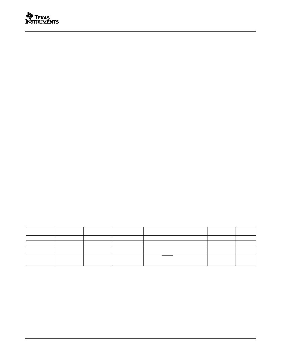
ORDERING INFORMATION
(1)
MAXIMUM
MAXIMUM
MAXIMUM
TRANSPORT
INTEGRAL
DIFFERENTIAL
OFFSET
PACKAGE
PACKAGE
TEMPERATURE
ORDERING
MODEL
MEDIA
LINEARITY
LINEARITY
ERROR
TYPE
DESIGNATOR
RANGE
INFORMATION
QUANTITY
(LSB)
(LSB)
(mV)
ADS8327IPW
Tube 90
ADS8327I
±3
≠1/+2
±0.8
TSSOP-16
PW
≠40∞C to 85∞C
Tape and reel
ADS8327IPWR
2000
ADS8327IBPW
Tube 90
ADS8327IB
±2
±1
±0.5
TSSOP-16
PW
≠40∞C to 85∞C
Tape and reel
ADS8327IBPWR
2000
ADS8328IPW
Tube 90
ADS8328I
±3
≠1/+2
±0.8
TSSOP-16
PW
≠40∞C to 85∞C
Tape and reel
ADS8328IPWR
2000
ADS8328IBPW
Tube 90
ADS8328IB
±2
±1
±0.5
TSSOP-16
PW
≠40∞C to 85∞C
Tape and reel
ADS8328IBPWR
2000
(1)
For the most current package and ordering information, see the Package Option Addendum at the end of this document, or see the TI
website at www.ti.com.
over operating free-air temperature range unless otherwise noted
(1)
UNIT
+IN to AGND
≠0.3 V to +VA + 0.3 V
Voltage
≠IN to AGND
≠0.3 V to +VA + 0.3 V
+VA to AGND
≠0.3 V to 7 V
Voltage range
+VBD to BDGND
≠0.3 V to 7 V
AGND to BDGND
≠0.3 V to 0.3 V
Digital input voltage to BDGND
≠0.3 V to +VBD + 0.3 V
Digital output voltage to BDGND
≠0.3 V to +VBD + 0.3 V
T
A
Operating free-air temperature range
≠40∞C to 85∞C
T
stg
Storage temperature range
≠65∞C to 150∞C
Junction temperature (T
J
max)
150∞C
Vapor phase (60 sec)
215∞C
Lead temperature, soldering
Infrared (15 sec)
220∞C
TSSOP-16
Package
Power dissipation
(T
J
Max - T
A
)/
JA
JA
thermal impedance
47∞C/W
(1)
Stresses beyond those listed under absolute maximum ratings may cause permanent damage to the device. These are stress ratings
only, and functional operation of the device at these or any other conditions beyond those indicated under recommended operating
conditions is not implied. Exposure to absolute-maximum-rated conditions for extended periods may affect device reliability.
2
Submit Documentation Feedback
www.ti.com
SPECIFICATIONS
ADS8327
ADS8328
SLAS415A ≠ APRIL 2006 ≠ REVISED MAY 2006
T
A
= ≠40∞C to 85∞C, +VA = 2.7 V, +VBD = +VA ◊ 1.5 to +1.65 V, V
ref
= 2.5 V, f
SAMPLE
= 500 kHz (unless otherwise noted)
PARAMETER
TEST CONDITIONS
MIN
TYP
MAX
UNIT
ANALOG INPUT
Full-scale input voltage
(1)
+IN ≠ (≠IN) or (+INx ≠ COM)
0
+V
ref
V
+IN, +IN0, +IN1
AGND ≠ 0.2
+VA + 0.2
Absolute input voltage
V
≠IN or COM
AGND ≠ 0.2
AGND + 0.2
Input capacitance
40
45
pF
No ongoing conversion,
Input leakage current
-1
1
nA
DC Input
At dc
108
Input channel isolation, ADS8328 only
dB
V
I
= ±1.25 V
pp
at 50 kHz
101
SYSTEM PERFORMANCE
Resolution
16
Bits
No missing codes
16
Bits
ADS8327IB,
≠2
±1.2
2
ADS8328IB
INL
Integral linearity
LSB
(2)
ADS8327I, ADS8328I
≠3
±2
3
ADS8327IB,
≠ 1
±0.6
1
Differential
ADS8328IB
DNL
LSB
(2)
linearity
ADS8327I, ADS8328I
≠1
±1
2
ADS8327IB,
≠ 0.5
±0.1
0.5
ADS8328IB
E
O
Offset error
(3)
mV
ADS8327I, ADS8328I
≠0.8
±0.1
0.8
Offset error drift
0.2
PPM/∞C
E
G
Gain error
≠ 0.25
≠0.07
0.25
%FSR
Gain error drift
0.3
PPM/∞C
At dc
70
CMRR
Common mode rejection ratio
dB
V
I
= 0.4 V
pp
at 1 MHz
50
Noise
33
µ
V RMS
PSRR
Power supply rejection ratio
At FFFFh output code
(3)
78
dB
SAMPLING DYNAMICS
t
CONV
Conversion time
18
CCLK
t
SAMPLE1
Manual trigger
3
Acquisition time
CCLK
t
SAMPLE2
Auto trigger
3
Throughput rate
500
kHz
Aperture delay
5
ns
Aperture jitter
10
ps
Step response
100
ns
Overvoltage recovery
100
ns
(1)
Ideal input span, does not include gain or offset error.
(2)
LSB means least significant bit
(3)
Measured relative to an ideal full-scale input [+IN ≠ (≠IN)] of 2.5 V when +VA = 2.7 V.
3
Submit Documentation Feedback
www.ti.com
ADS8327
ADS8328
SLAS415A ≠ APRIL 2006 ≠ REVISED MAY 2006
SPECIFICATIONS (continued)
T
A
= ≠40∞C to 85∞C, +VA = 2.7 V, +VBD = +VA ◊ 1.5 to +1.65 V, V
ref
= 2.5 V, f
SAMPLE
= 500 kHz (unless otherwise noted)
PARAMETER
TEST CONDITIONS
MIN
TYP
MAX
UNIT
DYNAMIC CHARACTERISTICS
V
IN
= 2.5 V
pp
at 10 kHz
-98
THD
Total harmonic distortion
(4)
dB
V
IN
= 2.5 V
pp
at 100 kHz
-83.5
V
IN
= 2.5 V
pp
at 10 kHz
88.5
SNR
Signal-to-noise ratio
dB
V
IN
= 2.5 V
pp
at 100 kHz
85
V
IN
= 2.5 V
pp
at 10 kHz
88.5
SINAD
Signal-to-noise + distortion
dB
V
IN
= 2.5 V
pp
at 100 kHz
81
V
IN
= 2.5 V
pp
at 10 kHz
101
SFDR
Spurious free dynamic range
dB
V
IN
= 2.5 V
pp
at 100 kHz
84
-3dB Small signal bandwidth
30
MHz
CLOCK
Internal conversion clock frequency
10.5
11
12.2
MHz
Used as I/O clock only
33
SCLK External serial clock
MHz
As I/O clock and conversion clock
1
21
EXTERNAL VOLTAGE REFERENCE INPUT
V
ref
(REF+ ≠ REF≠)
3.6 V
+VA
2.7 V
0.3
2.525
Input reference
V
ref
V
range
(REF≠) ≠ AGND
≠0.1
0.1
Resistance
(5)
Reference input
80
k
DIGITAL INPUT/OUTPUT
Logic family -- CMOS
V
IH
High-level input voltage
(+VA ◊ 1.5) V
+VBD
1.65 V
0.65
◊
(+VBD)
+VBD + 0.3
V
V
IL
Low-level input voltage
(+VA ◊ 1.5) V
+VBD
1.65 V
≠0.3
0.35
◊
(+VBD)
V
I
I
Input current
V
I
= +VBD or BDGND
-50
50
nA
C
i
Input capacitance
5
pF
(+VA ◊ 1.5) V
+VBD
1.65 V,
V
OH
High-level output voltage
+VBD ≠ 0.6
+VBD
V
I
O
= 100
µ
A
(+VA ◊ 1.5) V
+VBD
1.65 V,
V
OL
Low-level output voltage
0
0.4
V
I
O
= 100
µ
A
C
O
Output capacitance
5
pF
C
L
Load capacitance
30
pF
Data format -- straight binary
POWER SUPPLY REQUIREMENTS
+VBD
1.65
+VA
1.5 ◊ (+VA)
V
Power supply
voltage
+VA
2.7
3.6
V
500-kHz Sample rate
3.8
5
mA
Supply current
Nap mode
0.2
0.4
PD Mode
2
50
nA
Buffer I/O supply current
500 KSPS
0.2
mA
Power dissipation
+VA = 2.7 V, +VBD = 1.8 V
10.6
14
mW
TEMPERATURE RANGE
T
A
Operating free-air temperature
≠40
85
∞C
(4)
Calculated on the first nine harmonics of the input frequency
(5)
Can vary ±30%
4
Submit Documentation Feedback
www.ti.com
SPECIFICATIONS
ADS8327
ADS8328
SLAS415A ≠ APRIL 2006 ≠ REVISED MAY 2006
T
A
= ≠40∞C to 85∞C, +VA = 5 V, +VBD = +5.5 V to +1.65 V, V
ref
= 4.096 V, f
SAMPLE
= 500 kHz (unless otherwise noted)
PARAMETER
TEST CONDITIONS
MIN
TYP
MAX
UNIT
ANALOG INPUT
Full-scale input voltage
(1)
+IN ≠ (≠IN) or (+INx ≠ COM)
0
+V
ref
V
+IN, +IN0, +IN1
AGND ≠ 0.2
+VA + 0.2
Absolute input voltage
V
≠IN or COM
AGND ≠ 0.2
AGND + 0.2
Input capacitance
40
45
pF
No ongoing conversion,
Input leakage current
-1
1
nA
DC Input
At dc
109
Input channel isolation, ADS8328 only
dB
V
I
= ±1.25 V
pp
at 50 kHz
101
SYSTEM PERFORMANCE
Resolution
16
Bits
No missing codes
16
Bits
ADS8327IB,
≠2
±1.5
2
ADS8328IB
INL
Integral linearity
LSB
(2)
ADS8327I, ADS8328I
-3
±2
3
ADS8327IB,
≠ 1
±0.7
1
Differential
ADS8328IB
DNL
LSB
(2)
linearity
ADS8327I, ADS8328I
≠1
±1
2
ADS8327IB,
≠ 1
±0.4
1
ADS8328IB
E
O
Offset error
(3)
mV
ADS8327I, ADS8328I
≠1.25
±0.4
1.25
Offset error drift
0.5
PPM/∞C
E
G
Gain error
≠ 0.25
≠0.07
0.25
%FSR
Gain error drift
0.3
PPM/∞C
At dc
70
CMRR
Common mode rejection ratio
dB
V
I
= 1 V
pp
at 1 MHz
50
Noise
33
µ
V RMS
PSRR
Power supply rejection ratio
At FFFFh output code
(3)
78
dB
SAMPLING DYNAMICS
t
CONV
Conversion time
18
CCLK
t
SAMPLE
Manual trigger
3
1
Acquisition time
CCLK
t
SAMPLE
Auto trigger
3
2
Throughput rate
500
kHz
Aperture delay
5
ns
Aperture jitter
10
ps
Step response
100
ns
Overvoltage recovery
100
ns
(1)
Ideal input span, does not include gain or offset error.
(2)
LSB means least significant bit
(3)
Measured relative to an ideal full-scale input [+IN ≠ (≠IN)] of 4.096 V when +VA = 5 V.
5
Submit Documentation Feedback
www.ti.com
ADS8327
ADS8328
SLAS415A ≠ APRIL 2006 ≠ REVISED MAY 2006
SPECIFICATIONS (continued)
T
A
= ≠40∞C to 85∞C, +VA = 5 V, +VBD = +5.5 V to +1.65 V, V
ref
= 4.096 V, f
SAMPLE
= 500 kHz (unless otherwise noted)
PARAMETER
TEST CONDITIONS
MIN
TYP
MAX
UNIT
DYNAMIC CHARACTERISTICS
V
IN
= 4.096 V
pp
at 10 kHz
-96
THD
Total harmonic distortion
(4)
V
IN
= 4.096 V
pp
at 100 kHz,
ADS8327/28IB
-95.7
dB
V
IN
= 4.096 V
pp
at 100 kHz,
ADS8327/28I
-95.7
V
IN
= 4.096 V
pp
at 10 kHz
91
SNR
Signal-to-noise ratio
dB
V
IN
= 4.096 V
pp
at 100 kHz
89
V
IN
= 4.096 V
pp
at 10 kHz
91
SINAD
Signal-to-noise + distortion
dB
V
IN
= 4.096 V
pp
at 100 kHz
88
V
IN
= 4.096 V
pp
at 10 kHz
100
SFDR
Spurious free dynamic range
V
IN
= 4.096 V
pp
at 100 kHz,
ADS8327/28IB
98.8
dB
V
IN
= 4.096 V
pp
at 100 kHz,
ADS8327/28I
98.8
-3dB Small signal bandwidth
30
MHz
CLOCK
Internal conversion clock frequency
10.9
12
12.6
MHz
Used as I/O clock only
50
SCLK External serial clock
MHz
As I/O clock and conversion clock
1
21
EXTERNAL VOLTAGE REFERENCE INPUT
V
ref
(REF+ ≠ REF≠)
5.5 V
+VA
4.5 V
0.3
4.096
4.2
Input reference
V
ref
V
range
(REF≠) ≠ AGND
≠0.1
0.1
Resistance
(5)
Reference input
80
k
DIGITAL INPUT/OUTPUT
Logic family -- CMOS
V
IH
High-level input voltage
5.5 V
+VBD
4.5 V
0.65 ◊ (+VBD)
+VBD + 0.3
V
V
IL
Low-level input voltage
5.5 V
+VBD
4.5 V
≠0.3
0.35 ◊ (+VBD)
V
I
I
Input current
V
I
= +VBD or BDGND
-50
50
nA
C
i
Input capacitance
5
pF
5.5 V
+VBD
4.5 V,
V
OH
High-level output voltage
+VBD ≠ 0.6
+VBD
V
I
O
= 100
µ
A
5.5 V
+VBD
4.5 V,
V
OL
Low-level output voltage
0
0.4
V
I
O
= 100
µ
A
C
O
Output capacitance
5
pF
C
L
Load capacitance
30
pF
Data format -- straight binary
POWER SUPPLY REQUIREMENTS
+VBD
1.65
3.3
5.5
V
Power supply
voltage
+VA
4.5
5
5.5
V
500-kHz Sample rate
5
6.2
mA
Supply current
Nap mode
0.3
0.5
PD Mode
6
50
nA
Buffer I/O supply current
500 KSPS
1
mA
+VA = 5 V, +VBD = 5 V
30
38.5
Power dissipation
mW
+VA = 5 V, +VBD = 1.8 V
25.4
32
TEMPERATURE RANGE
T
A
Operating free-air temperature
≠40
85
∞C
(4)
Calculated on the first nine harmonics of the input frequency
(5)
Can vary ±30%
6
Submit Documentation Feedback
www.ti.com
TIMING CHARACTERISTICS
ADS8327
ADS8328
SLAS415A ≠ APRIL 2006 ≠ REVISED MAY 2006
All specifications typical at ≠40∞C to 85∞C, +VA = 2.7 v, +VBD = 1.8 V
(1) (2)
PARAMETER
MIN
TYP
MAX
UNIT
External,
0.5
10.5
f
CCLK
= 1/2 f
SCLK
f
CCLK
Frequency, conversion clock, CCLK
MHz
Internal
10.5
12
12.2
t
su(CSF-EOC)
Setup time, falling edge of CS to EOC
1
CCLK
t
h(CSF-EOC)
Hold time, falling edge of CS to EOC
0
ns
t
wL(CONVST)
Pulse duration, CONVST low
40
ns
t
su(CSF-EOS)
Setup time, falling edge of CS to EOS
20
ns
t
h(CSF-EOS)
Hold time, falling edge of CS to EOS
20
ns
t
su(CSR-EOS)
Setup time, rising edge of CS to EOS
20
ns
t
h(CSR-EOS)
Hold time, rising edge of CS to EOS
20
ns
t
c(SCLK)
t
su(CSF-SCLK1R)
Setup time, falling edge of CS to SCLK
5
ns
- 5
t
c(SCLK)
t
wL(SCLK)
Pulse duration, SCLK low
8
ns
- 8
t
c(SCLK)
t
wH(SCLK)
Pulse duration, SCLK high
8
ns
- 8
I/O Clock only
30
I/O and conversion clock
47.6
1000
t
c(SCLK)
Cycle time, SCLK
ns
I/O Clock, chain mode
30
I/O and conversion clock,
47.6
1000
chain mode
Delay time, falling edge of SCLK to SDO
t
d(SCLKF-SDOINVALID)
10-pF Load
8
ns
invalid
Delay time, falling edge of SCLK to SDO
t
d(SCLKF-SDOVALID)
10-pF Load
25
ns
valid
Delay time, falling edge of CS to SDO valid,
t
d(CSF-SDOVALID)
10-pF Load
25
ns
SDO MSB output
t
su(SDI-SCLKF)
Setup time, SDI to falling edge of SCLK
8
ns
t
h(SDI-SCLKF)
Hold time, SDI to falling edge of SCLK
4
ns
Delay time, rising edge of CS/FS to SDO
t
d(CSR-SDOZ)
5
ns
3-state
Setup time, last falling edge of SCLK before
t
su(lastSCLKF-CSR)
10
ns
rising edge of CS/FS
Delay time, CDI high to SDO high in daisy
t
d(SDO-CDI)
10-pF Load, chain mode
25
ns
chain mode
(1)
All input signals are specified with t
r
= t
f
= 1.5 ns (10% to 90% of V
DD
) and timed from a voltage level of (V
IL
+ V
IH
)/2.
(2)
See timing diagrams.
7
Submit Documentation Feedback
www.ti.com
TIMING CHARACTERISTICS
ADS8327
ADS8328
SLAS415A ≠ APRIL 2006 ≠ REVISED MAY 2006
All specifications typical at ≠40∞C to 85∞C, +VA = +VBD = 5 V
(1) (2)
PARAMETER
MIN
TYP
MAX
UNIT
External,
0.5
10.5
f
CCLK
= 1/2 f
SCLK
f
CCLK
Frequency, conversion clock, CCLK
MHz
Internal
10.9
12
12.6
t
su(CSF-EOC)
Setup time, falling edge of CS to EOC
1
CCLK
t
h(CSF-EOC)
Hold time, falling edge of CS to EOC
0
ns
t
wL(CONVST)
Pulse duration, CONVST low
40
ns
t
su(CSF-EOS)
Setup time, falling edge of CS to EOS
20
ns
t
h(CSF-EOS)
Hold time, falling edge of CS to EOS
20
ns
t
su(CSR-EOS)
Setup time, rising edge of CS to EOS
20
ns
t
h(CSR-EOS)
Hold time, rising edge of CS to EOS
20
ns
t
c(SCLK)
-
t
su(CSF-SCLK1R)
Setup time, falling edge of CS to SCLK
5
ns
5
t
c(SCLK)
-
t
wL(SCLK)
Pulse duration, SCLK low
8
ns
8
t
c(SCLK)
-
t
wH(SCLK)
Pulse duration, SCLK high
8
ns
8
I/O Clock only
20
I/O and conversion clock
47.6
1000
t
c(SCLK)
Cycle time, SCLK
ns
I/O Clock, chain mode
20
I/O and conversion clock,
47.6
1000
chain mode
Delay time, falling edge of SCLK to SDO
t
d(SCLKF-SDOINVALID)
10-pF Load
5
ns
invalid
Delay time, falling edge of SCLK to SDO
t
d(SCLKF-SDOVALID)
10-pF Load
12
ns
valid
Delay time, falling edge of CS to SDO
t
d(CSF-SDOVALID)
10-pF Load
12
ns
valid, SDO MSB output
t
su(SDI-SCLKF)
Setup time, SDI to falling edge of SCLK
8
ns
t
h(SDI-SCLKF)
Hold time, SDI to falling edge of SCLK
4
ns
Delay time, rising edge of CS/FS to SDO
t
d(CSR-SDOZ)
5
ns
3-state
Setup time, last falling edge of SCLK
t
su(lastSCLKF-CSR)
10
ns
before rising edge of CS/FS
Delay time, CDI high to SDO high in daisy
t
d(SDO-CDI)
10-pF Load, chain mode
16
ns
chain mode
(1)
All input signals are specified with t
r
= t
f
= 1.5 ns (10% to 90% of V
DD
) and timed from a voltage level of (V
IL
+ V
IH
)/2.
(2)
See timing diagrams.
8
Submit Documentation Feedback
www.ti.com
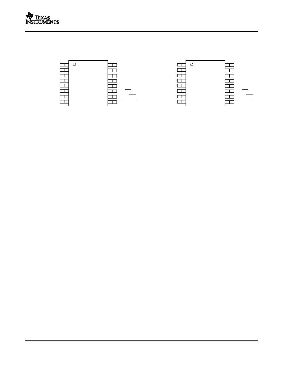
PIN ASSIGNMENTS
1
2
3
4
5
6
7
8
16
15
14
13
12
11
10
9
+VA
NC
+IN
-IN
AGND
REF-
REF+ (REFIN)
NC (REFOUT)
+VBD
SCLK
BDGND
SDO
SDI
FS/CS
EOC/INT
CONVST
ADS8327
PW PACKAGE
(TOP VIEW)
1
2
3
4
5
6
7
8
16
15
14
13
12
11
10
9
+VA
+IN1
+IN0
COM
AGND
REF-
REF+ (REFIN)
NC (REFOUT)
+VBD
SCLK
BDGND
SDO
SDI
FS/CS
EOC/INT
CONVST
ADS8328
PW PACKAGE
(TOP VIEW)
NC - No internal connection
ADS8327
ADS8328
SLAS415A ≠ APRIL 2006 ≠ REVISED MAY 2006
9
Submit Documentation Feedback
www.ti.com
ADS8327
ADS8328
SLAS415A ≠ APRIL 2006 ≠ REVISED MAY 2006
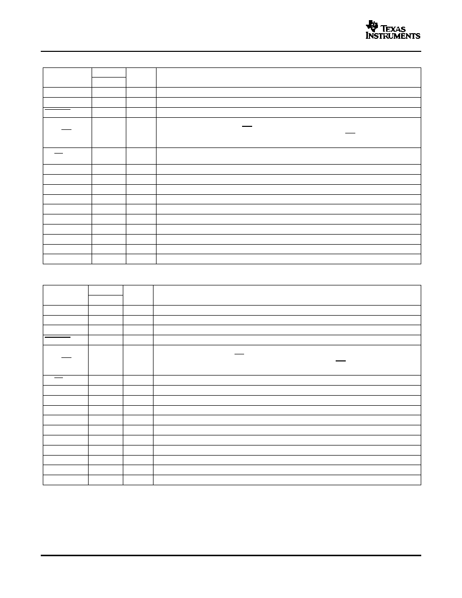
ADS8327 Terminal Functions
NO.
NAME
I/O
DESCRIPTION
TSSOP
AGND
5
≠
Analog ground
BDGND
14
≠
Interface ground
CONVST
9
Freezes sample and hold, starts conversion with next rising edge of internal clock
Status output. If programmed as EOC, this pin is low (default) when a conversion is in progress.
If programmed as an interrupt (INT), this pin is low for a preprogrammed duration after the end
EOC/ INT/ CDI
10
O
of conversion and a valid data is to be output. The polarity of EOC or INT is programmable. This
pin can also be used as a chain data input when the device is operated in chain mode.
Frame sync signal for TMS320 DSP serial interface or chip select input for SPI interface slave
FS/CS
11
select (SS-).
+IN
3
I
Non inverting input
-IN
4
I
Inverting input, usually connected to ground
NC
2,8
≠
No connection.
REF+
7
I
External reference input.
REF-
6
Connect to AGND through individual via.
SCLK
15
Clock for serial interface
SDI
12
I
Serial data in
SDO
13
O
Serial data out
+VA
1
Analog supply, +2.7 V to +5.5 VDC.
+VBD
16
Interface supply
ADS8328 Terminal Functions
NO.
NAME
I/O
DESCRIPTION
TSSOP
AGND
5
≠
Analog ground
BDGND
14
≠
Interface ground
COM
4
I
Common inverting input, usually connected to ground
CONVST
9
Freezes sample and hold, starts conversion with next rising edge of internal clock
Status output. If programmed as EOC, this pin is low (default) when a conversion is in progress. If
programmed as an interrupt (INT), this pin is low for a preprogrammed duration after the end of
EOC/ INT/ CDI
10
O
conversion and a valid data is to be output. The polarity of EOC or INT is programmable. This pin
can also be used as a chain data input when the device is operated in chain mode.
FS/CS
11
Frame sync signal for TMS320 DSP serial interface or chip select input for SPI interface
+IN1
2
I
Second noninverting input.
+IN0
3
I
First noninverting input
NC
8
≠
No connection.
REF+
7
I
External reference input.
REF-
6
Connect to AGND through individual via.
SCLK
15
Clock for serial interface
SDI
12
I
Serial data in (conversion start and reset possible)
SDO
13
O
Serial data out
+VA
1
Analog supply, +2.7 V to +5.5 VDC.
+VBD
16
Interface supply
10
Submit Documentation Feedback
www.ti.com
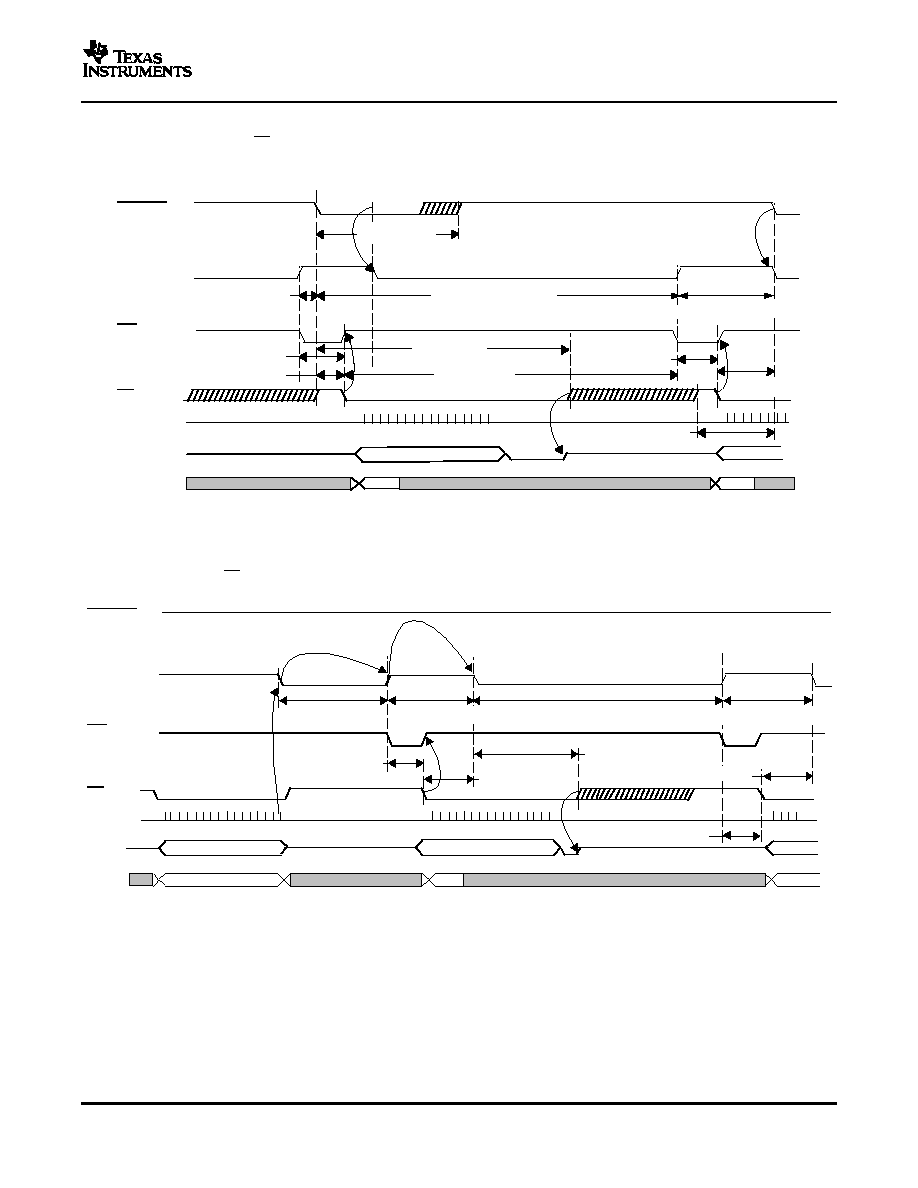
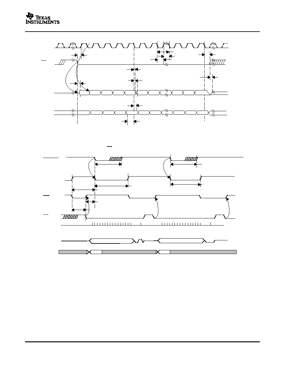
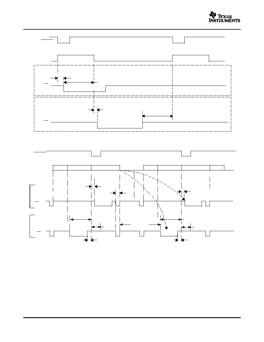
t
SAMPLE1
= 3 CCLKs min
t
d(CRS-EOS)
= 20 ns min
t
CONV
= 18 CCLKs
t
h(CSF-EOC)
t
h(CSF-EOC)
t
h(CSR-EOS)
t
h(CSF-EOS)
t
su(CSF-EOC)
t
su(CSF-EOS)
t
SAMPLE1
= 3 CCLKs min
t
wL(CONVST)
EOC
(active low)
MANUAL TRIGGER / READ While Sampling
(use internal CCLK, EOC and
polarity programmed as active low)
INT
(active low)
INT
/FS
CS
SCLK
SDO
SDI
CONVST
Nth
Nth
EOC
EOS
EOC
EOS
1101b
1101b
Nth!1th
Nth
READ Result
READ Result
1 . . . . . . . . . . . . . . . . . . . . 16
1
1101b
EOS
EOC
EOS
EOC
EOS
1110b. . . . . . . . . . . . . .
1101b
Nth
CONFIGURE
READ Result
N ! 1th
N ! 1th
Nth
READ Result
EOC
(active low)
AUTO TRIGGER / READ While Sampling
(use internal CCLK, EOC and
polarity programmed as active low)
INT
(active low)
INT
/FS
CS
SCLK
SDO
SDI
= 1
CONVST
t
SAMPLE2
= 3 CCLKs
t
SAMPLE2
= 3 CCLKs
t
CONV
= 18 CCLKs
t
CONV
= 18 CCLKs
t
h(CSF-EOC)
t
h(CSF-EOC)
t
h(CSF-EOS)
t
su(CSF-EOS)
t
su(CSF-EOS)
1 . . . . . . . . . . . . . . . . . . .16
1 . . . . . . . . . . . . . . . . . . .16
1
ADS8327
ADS8328
SLAS415A ≠ APRIL 2006 ≠ REVISED MAY 2006
Figure 1. Timing for Conversion and Acquisition Cycles for Manual Trigger (read while sampling)
Figure 2. Timing for Conversion and Acquisition Cycles for Autotrigger (read while sampling)
11
Submit Documentation Feedback
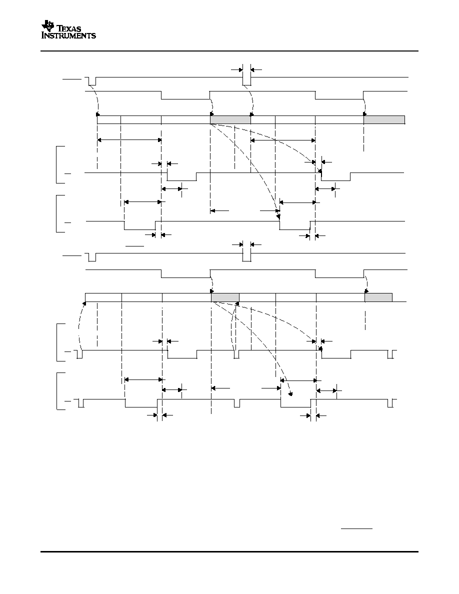
www.ti.com
1101b
1101b
EOC
EOS
EOS
N th
Nth
N ! 1th
Nth
N + 1th
N ! 1th
READ Result
READ Result
EOC
(active low)
MANUAL TRIGGER / READ While Converting
(use internal CCLK, EOC and
polarity programmed as active low)
INT
(active low)
INT
/FS
CS
SCLK
SDO
SDI
CONVST
t
wL(CONVST)
t
SAMPLE1
= 3 CCLKs min
t
CONV
= 18 CCLKs
t
h(CSF-EOC)
t
h(CSF-EOS)
t
su(CSF-EOS)
t
su(CSR-EOS)
t
su(CSF-EOC)
1 . . . . . . . . . . . . . . . . . . . .16
1
1 . . . . . . . . . . . . . . . . . . .16
EOC
EOS
EOC
EOS
EOS
1110b . . . . . . . . . . . . . . .
??
1101b
1101b
N!1 th
N th
N!1 th
READ Result
READ Result
CONFIGURE
Nth
N + 1th
EOC
(active low)
AUTO TRIGGER / READ While Converting
(use internal CCLK, EOC and
polarity programmed as active low)
INT
(active low)
INT
/FS
CS
SCLK
SDO
SDI
= 1
CONVST
t
CONV
= 18 CCLKs
t
h(CSR-EOS)
t
su(CSF-EOS)
t
h(CSF-EOS)
t
SAMPLE2
= 3 CCLKs min
t
CONV
= 18 CCLKs
t
h(CSF-EOS)
t
su(CSR-EOS)
t
su(CSR-EOS)
t
SAMPLE2
= 3 CCLKs min
1 . . . . . . . . . . . . . . . . . . 16
1 . . . . . . . . . . . . . . . . . . 16
ADS8327
ADS8328
SLAS415A ≠ APRIL 2006 ≠ REVISED MAY 2006
Figure 3. Timing for Conversion and Acquisition Cycles for Manual Trigger (read while converting)
Figure 4. Timing for Conversion and Acquisition Cycles for Autotrigger (read while converting)
12
Submit Documentation Feedback
www.ti.com
1
2
3
5
4
6
7
15
16
14
MSB-1 MSB-2 MSB-3 MSB-4
MSB-5 MSB-6
LSB+2
LSB+1
LSB
MSB
MSB-1 MSB-2 MSB-3 MSB-4 MSB-5
MSB-6
LSB+2
LSB+1
LSB
MSB
t
su(CSF-SCLK1R)
CS/FS
t
d(CSF-SDOVALID)
t
su(SDI-SCLKF)
t
h(SDI-SCLKF)
t
d(SCLKF-SDOINVALID)
t
d(SCLKF-SDOVALID)
t
d(CSR-SDOZ)
t
su(LastSCLK-CSR)
t
wL(SCLK)
t
wH(SCLK)
t
c(SCLK)
SCLK
SDO
SDI
Hi-Z
1101b
1101b
MANUAL TRIGGER / READ While Sampling
(use internal CCLK
, EOC and INT active low, TAG enabled, auto channel select)
active high
Hi!Z
EOS
EOC
READ Result
READ Result
N!1th CH1
CONVST
INT
(active low)
EOC
(active low)
CS/FS
SCLK
SDO
SDI
Nth CH0
1 . . . . . . . . . . . . . . . . . . . . . . . 16
17
1 16
. . . . . . . . . . . . . . . . . . . . . . .
17
Nth CH0
Nth CH1
Nth CH0
Nth CH0
Hi!Z
TAG = 0
TAG = 1
t
wL(CONVST)
t
wL(CONVST)
t
SAMPLE1
= 3 CCLKs min
t
CONV
= 18 CCLKs
t
d(CSR-EOS)
=
20 ns MIN
t
CONV
= 18 CCLKs
t
h(CSF-EOC)
t
su(CSF-EOS)
ADS8327
ADS8328
SLAS415A ≠ APRIL 2006 ≠ REVISED MAY 2006
Figure 5. Detailed SPI Transfer Timing
Figure 6. Simplified Dual Channel Timing
13
Submit Documentation Feedback
www.ti.com
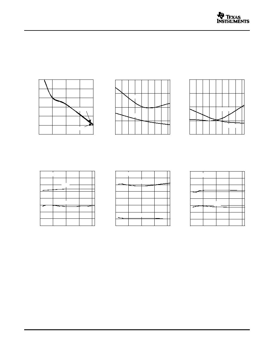
TYPICAL CHARACTERISTICS
80
85
90
95
100
105
110
0
50
100
150
200
F -Frequency - kHz
+VA = 5 V
+VA = 2.7
Crosstalk - dB
1.4
1.5
1.6
1.7
1.8
-40
-25
-10
5
20
35
50
65
80
T
- Free-Air Temperature - C
A
INL
- LSB
+VA = 2.7 V
+VA = 5 V
0.5
0.6
0.7
0.8
0.9
-40
-25 -10
5
20
35
50
65
80
T - Free-Air Temperature - C
A
+VA = 5 V
+VA = 2.7
DNL
- LSB
-2
-1.5
-1
-0.5
0
0.5
1
1.5
2
0
5
10
15
20
External Clock Frequency - MHz
MAX
MIN
+VA = 5 V
DNL
- LSB
-2
-1.5
-1
-0.5
0
0.5
1
1.5
2
0
5
10
15
20
External Clock Frequency - MHz
Max
Min
DNL
- LSB
+VA = 2.7 V
-2
-1.5
-1
-0.5
0
0.5
1
1.5
2
0
5
10
15
20
External Clock Frequency - MHz
INL
- LSB
Min
Max
+VA = 5 V
ADS8327
ADS8328
SLAS415A ≠ APRIL 2006 ≠ REVISED MAY 2006
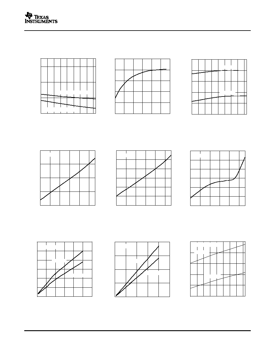
At ≠40∞C to 85∞C, V
ref
(REF+ ≠ REF≠) = 4.096 V when +VA = +VBD = 5 V or V
ref
(REF+ ≠ REF≠) = 2.5 V when
+VA = +VBD = 2.7 V, f
SCLK
= 21 MHz, f
i
= DC for DC curves, f
i
= 100 kHz for AC curves (unless otherwise
noted)
CROSSTALK
DIFFERENTIAL NONLINEARITY
INTEGRAL NONLINEARITY
vs
vs
vs
FREQUENCY
FREE-AIR TEMPERATURE
FREE-AIR TEMPERATURE
Figure 7.
Figure 8.
Figure 9.
DIFFERENTIAL NONLINEARITY
INTEGRAL NONLINEARITY
DIFFERENTIAL NONLINEARITY
vs
vs
vs
EXTERNAL CLOCK FREQUENCY
EXTERNAL CLOCK FREQUENCY
EXTERNAL CLOCK FREQUENCY
Figure 10.
Figure 11.
Figure 12.
14
Submit Documentation Feedback
www.ti.com
-2
-1.5
-1
-0.5
0
0.5
1
1.5
2
0
5
10
15
20
25
External Clock Frequency - MHz
INL
- LSB
Min
Max
+VA = 2.7 V
0
0.2
0.4
0.6
0.8
1
-40
-25
-10
5
20
35
50
65
80
T
- Free-Air Temperature - C
A
Offset V
oltage - mV
+VA = 2.7
+VA = 5 V
0
0.2
0.4
0.6
0.8
1
2.7
3.2
3.7
4.2
4.7
5.2
+VA - Supply Voltage - V
Offset V
oltage - mV
-80
-78
-76
-74
-72
-70
0
20
40
60
80
100
Supply Ripple Frequency - kHz
PSRR - Power Supply Rejection Ratio - dB
+VA = 5 V
+VA = 2.7 V
+VA - Supply Voltage - V
-0.075
-0.073
-0.070
-0.068
-0.065
2.7
3.2
3.7
4.2
4.7
5.2
Offset V
oltage
mV
Change -
-0.075
-0.073
-0.070
-0.068
-0.065
-40
-25
-10
5
20
35
50
65
80
T - Free-Air Temperature - C
A
Gain Error - % FSR
+VA = 5 V
+VA = 2.7
84
86
88
90
92
0
20
40
60
80
100
f - Input Frequency - kHz
i
SNR - Signal-T
o-Noise Ratio - dB
+VA = 2.7 V
+VA = 5 V
-80
-85
-90
-95
-100
-150
0
20
40
60
80
100
f - Input Frequency - kHz
i
THD - T
otal Harmonic Distortion - dB
+VA = 5 V
+VA = 2.7 V
80
82
84
86
88
90
92
0
20
40
60
80
100
f - Input Frequency - kHz
i
SINAD - Signal-T
o-Noise and Distortion - dB
+VA = 5 V
+VA = 2.7 V
ADS8327
ADS8328
SLAS415A ≠ APRIL 2006 ≠ REVISED MAY 2006
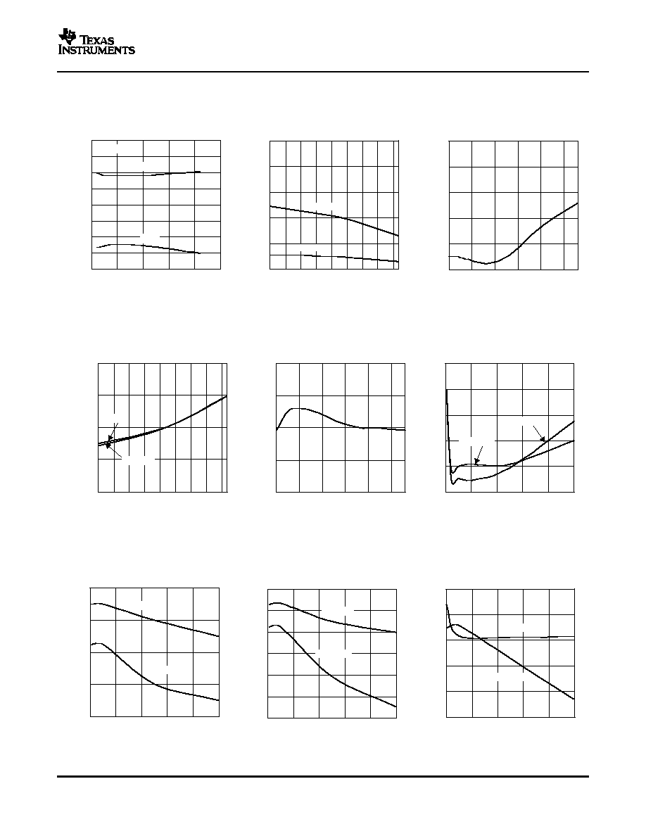
TYPICAL CHARACTERISTICS (continued)
INTEGRAL NONLINEARITY
OFFSET VOLTAGE
OFFSET VOLTAGE
vs
vs
vs
EXTERNAL CLOCK FREQUENCY
FREE-AIR TEMPERATURE
SUPPLY VOLTAGE
Figure 13.
Figure 14.
Figure 15.
GAIN ERROR
GAIN ERROR
POWER SUPPLY REJECTION
vs
vs
RATIO
FREE-AIR TEMPERATURE
SUPPLY VOLTAGE
vs
SUPPLY RIPPLE FREQUENCY
Figure 16.
Figure 17.
Figure 18.
SIGNAL-TO-NOISE RATIO
SIGNAL-TO-NOISE AND
TOTALHARMONIC DISTORTION
vs
DISTORTION
vs
INPUT FREQUENCY
vs
INPUT FREQUENCY
INPUT FREQUENCY
Figure 19.
Figure 20.
Figure 21.
15
Submit Documentation Feedback
www.ti.com
72
76
80
84
88
92
0
1
2
3
4
5
Full Scale Range - V
SINAD - Signal-T
o-Noise and Distortion - dB
5 V
2.7 V
10 kHz Input
72
76
80
84
88
92
0
1
2
3
4
5
Full Scale Range - V
SNR - Signal-T
o-Noise Ratio - dB
2.7 V
5 V
10 kHz Input
80
85
90
95
100
105
110
0
20
40
60
80
f - Input Frequency - kHz
i
SFDR - Spurious Free Dynamic Range - dB
100
+VA = 5 V
+VA = 2.7 V
-100
-96
-92
-88
0
1
2
3
4
5
Full Scale Range - V
THD - T
otal Harmonic Distortion -dB
10 kHz Input
5 V
2.7 V
10 KHz
90
92
94
96
98
100
102
0
1
2
3
4
5
Full Scale Range - V
SFDR - Spurious Free Dynamic Range - dB
2.7 V
5 V
-100
-98
-96
-94
-40
-25
-10
5
20
35
50
65
T
- Free-Air Temperature - C
A
THD - T
otal Harmonic Distortion - dB
+VA = 5 V, 100 kHz Input
+VA = 2.7 V, 10 kHz Input
80
87
88
89
90
91
92
-40 -25
-10
5
20
35
50
65
80
T
- Free-Air Temperature - C
A
SINAD - Signal-T
o-Noise and Distortion - dB
+VA =5 V, 100 kHz Input
+VA = 2.7 V, 10 kHz Input
87
88
89
90
91
92
-40 -25
-10
5
20
35
50
65
80
T
- Free-Air Temperature - C
A
SNR - Signal-T
o-Noise Ratio - dB
+VA = 5 V, 100 kHz Input
+VA = 2.7 V, 10 kHz Input
94
96
98
100
102
-40
-25
-10
5
20
35
50
65
80
T
- Free-Air Temperature - C
A
SFDR - Spurious Free Dynamic Range - dB
+VA = 5 V, 100 kHz Input
+VA = 2.7 V, 10 kHz Input
ADS8327
ADS8328
SLAS415A ≠ APRIL 2006 ≠ REVISED MAY 2006
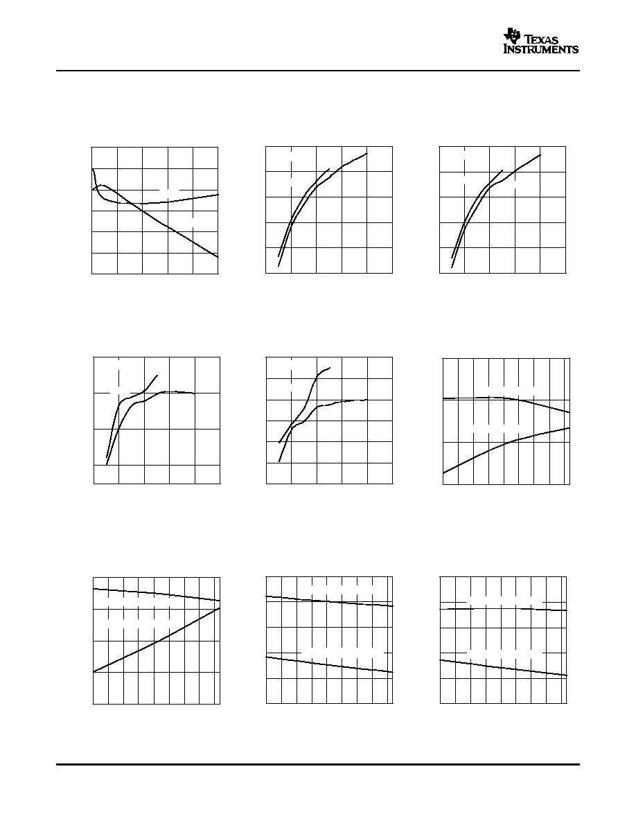
TYPICAL CHARACTERISTICS (continued)
SPURIOUS FREE DYNAMIC RANGE
SIGNAL-TO-NOISE RATIO
SIGNAL-TO-NOISE AND
vs
vs
DISTORTION
INPUT FREQUENCY
FULL SCALE RANGE
vs
FULL SCALE RANGE
Figure 22.
Figure 23.
Figure 24.
TOTAL HARMONIC DISTORTION
SPURIOUS FREE DYNAMIC RANGE
TOTAL HARMONIC DISTORTION
vs
vs
vs
FULL SCALE RANGE
FULL SCALE RANGE
FREE-AIR TEMPERATURE
Figure 25.
Figure 26.
Figure 27.
SPURIOUS FREE DYNAMIC RANGE
SIGNAL-TO-NOISE RATIO
SIGNAL-TO-NOISE AND
vs
vs
DISTORTION
FREE-AIR TEMPERATURE
FREE-AIR TEMPERATURE
vs
FREE-AIR TEMPERATURE
Figure 28.
Figure 29.
Figure 30.
16
Submit Documentation Feedback
www.ti.com
11.0
11.2
11.4
11.6
11.8
12
2.7
3.2
3.7
4.2
4.7
5.2
5.7
+VA - Supply Voltage - V
Internal Clock Frequency - MHz
14.3
14.5
14.7
-40 -25
-10
5
20
35
50
65
80
T
- Free-Air Temperature - C
A
ENOB - Effective Number of Bits - bits
+VA = 5 V, 100 kHz Input
+VA = 2.7 V, 10 kHz Input
14.9
11
11.2
11.4
11.6
11.8
12
-40
-25
-10
5
20
35
50
65
T
- Free-Air Temperature - C
A
Internal Clock Frequency - MHz
80
+VA = 2.7 V
+VA = 5 V
500 kSPS
3.6
4.1
4.6
5.1
5.6
2.7
3.2
3.7
4.2
4.7
5.2
+VA - Supply Voltage - V
Analog Supply Current - mA
PD Mode
0
2
4
6
8
10
12
2.7
3.2
3.7
4.2
4.7
5.2
+VA - Supply Voltage - V
Analog Supply Current - nA
200
220
240
260
280
300
320
2.7
3.2
3.7
4.2
4.7
5.2
+VA - Supply Voltage - V
Analog Supply Current -
A
m
NAP Mode
Analog Supply Current - mA
Autonap Mode
0
1
2
3
4
5
6
0
100
200
300
400
500
600
Sample Rate - kSPS
+VA = 2.7 V
+VA = 5 V
PD Mode
0
100
200
300
400
0
5
10
15
20
25
Sample Rate - kSPS
Analog Supply Current -
A
m
+VA = 5 V
+VA = 2.7 V
Analog Supply Current - mA
500 kSPS Sample Rate
3
3.5
4
4.5
5
5.5
-40
-25
-10
5
20
35
50
65
80
T
- Free-Air Temperature - C
A
+VA = 2.7 V
+VA = 5 V
ADS8327
ADS8328
SLAS415A ≠ APRIL 2006 ≠ REVISED MAY 2006
TYPICAL CHARACTERISTICS (continued)
EFFECTIVE NUMBER OF BITS
INTERNAL CLOCK FREQUENCY
INTERNAL CLOCK FREQUENCY
vs
vs
vs
FREE-AIR TEMPERATURE
SUPPLY VOLTAGE
FREE-AIR TEMPERATURE
Figure 31.
Figure 32.
Figure 33.
ANALOG SUPPLY CURRENT
ANALOG SUPPLY CURRENT
ANALOG SUPPLY CURRENT
vs
vs
vs
SUPPLY VOLTAGE
SUPPLY VOLTAGE
SUPPLY VOLTAGE
Figure 34.
Figure 35.
Figure 36.
ANALOG SUPPLY CURRENT
ANALOG SUPPLY CURRENT
ANALOG SUPPLY CURRENT
vs
vs
vs
SAMPLE RATE
SAMPLE RATE
FREE-AIR TEMPERATURE
Figure 37.
Figure 38.
Figure 39.
17
Submit Documentation Feedback
www.ti.com
Analog Supply Current - mA
NAP Mode
0
0.1
0.2
0.3
0.4
-40
-25
-10
5
20
35
50
65
80
T
- Free-Air Temperature - C
A
+VA = 5 V
+VA = 2.7
-3
-2
0
0.5
2
3
0
10000
20000
30000
40000
50000
60000
70000
INL
- Bits
Code
2.5
1.5
1
-0.5
-1
-1.5
-2.5
f = 500 kSPS,
+VA = 5 V,
V
= 4.096 V
i
ref
-2
-1.5
-1
-0.5
0
0.5
1
1.5
2
0
10000
20000
30000
40000
50000
60000
70000
f = 500 kSPS,
+VA = 5 V,
V
= 4.096 V
i
ref
DNL
- Bits
Code
ADS8327
ADS8328
SLAS415A ≠ APRIL 2006 ≠ REVISED MAY 2006
TYPICAL CHARACTERISTICS (continued)
ANALOG SUPPLY CURRENT
vs
FREE-AIR TEMPERATURE
Figure 40.
INL
DNL
Figure 41.
Figure 42.
18
Submit Documentation Feedback
www.ti.com
-2.5
-2
-0.5
0
1
2
3
0
10000
20000
30000
40000
50000
60000
70000
INL
- Bits
Code
1.5
2.5
0.5
-1
-1.5
3
f = 500 kSPS,
+VA = 2.7 V,
V
= 2.5 V
i
ref
-2
-1.5
-1
-0.5
0
0.5
1
1.5
2
0
10000
DNL
- Bits
20000
30000
40000
50000
60000
70000
Code
f = 500 kSPS,
+VA = 2.7 V,
V
= 2.5 V
i
ref
-160
-140
-120
-100
-80
-60
-40
-20
0
0
50
100
150
200
250
1 kHz Input,+VA = 2.7 V,
V
= 2.5 V, f = 500 kSPS
ref
s
f - Frequency - kHz
Amplitude - dB
-160
-140
-120
-100
-80
-60
-40
-20
0
0
50
100
150
200
250
10 kHz Input,+VA = 2.7 V,
V
= 2.5 V, f = 500 kSPS
ref
s
f - Frequency - kHz
Amplitude - dB
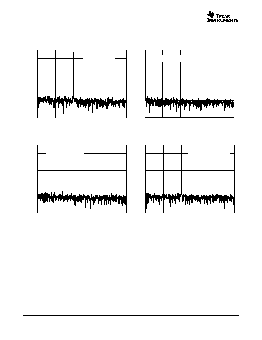
ADS8327
ADS8328
SLAS415A ≠ APRIL 2006 ≠ REVISED MAY 2006
TYPICAL CHARACTERISTICS (continued)
INL
DNL
Figure 43.
Figure 44.
FFT
FFT
Figure 45.
Figure 46.
19
Submit Documentation Feedback
www.ti.com
1 kHz Input,+VA = 5 V,
V
= 4.096 V, f = 500 kSPS
ref
s
-160
-140
-120
-100
-80
-60
-40
-20
0
0
50
100
150
200
250
f - Frequency - kHz
Amplitude - dB
100 kHz Input,
+VA = 2.7 V, V
= 2.5 V,
f = 500 kSPS
ref
s
-160
-140
-120
-100
-80
-60
-40
-20
0
0
50
100
150
200
250
f - Frequency - kHz
Amplitude - dB
-160
-140
-120
-100
-80
-60
-40
-20
0
0
50
100
150
200
250
10 kHz Input,+VA = 5 V,
V
= 4.096 V, f = 500 kSPS
ref
s
f - Frequency - kHz
Amplitude - dB
-160
-140
-120
-100
-80
-60
-40
-20
0
0
50
100
150
200
250
100 kHz Input,+VA = 5 V,
V
= 4.096 V, f = 500 kSPS
ref
s
f - Frequency - kHz
Amplitude - dB
THEORY OF OPERATION
ADS8327
ADS8328
SLAS415A ≠ APRIL 2006 ≠ REVISED MAY 2006
TYPICAL CHARACTERISTICS (continued)
FFT
FFT
Figure 47.
Figure 48.
FFT
FFT
Figure 49.
Figure 50.
The ADS8327/28 is a high-speed, low power, successive approximation register (SAR) analog-to-digital
converter (ADC) that uses an external reference. The architecture is based on charge redistribution, which
inherently includes a sample/hold function.
The ADS8327/28 has an internal clock that is used to run the conversion but can also be programmed to run the
conversion based on the external serial clock, SCLK.
The ADS8327 has one analog input. The analog input is provided to two input pins: +IN and -IN. When a
conversion is initiated, the differential input on these pins is sampled on the internal capacitor array. While a
conversion is in progress, both +IN and -IN inputs are disconnected from any internal function.
The ADS8328 has two inputs. Both inputs share the same common pin - COM. The negative input is the same
as the -IN pin for the ADS8327. The ADS8328 can be programmed to select a channel manually or can be
programmed into the auto channel select mode to sweep between channel 0 and 1 automatically.
20
Submit Documentation Feedback
www.ti.com
ANALOG INPUT
Device in Hold Mode
AGND
150
W
+IN
-IN
AGND
+VA
150
W
4 pF
4 pF
40 pF
40 pF
Driver Amplifier Choice
Bipolar to Unipolar Driver
ADS8327
ADS8328
SLAS415A ≠ APRIL 2006 ≠ REVISED MAY 2006
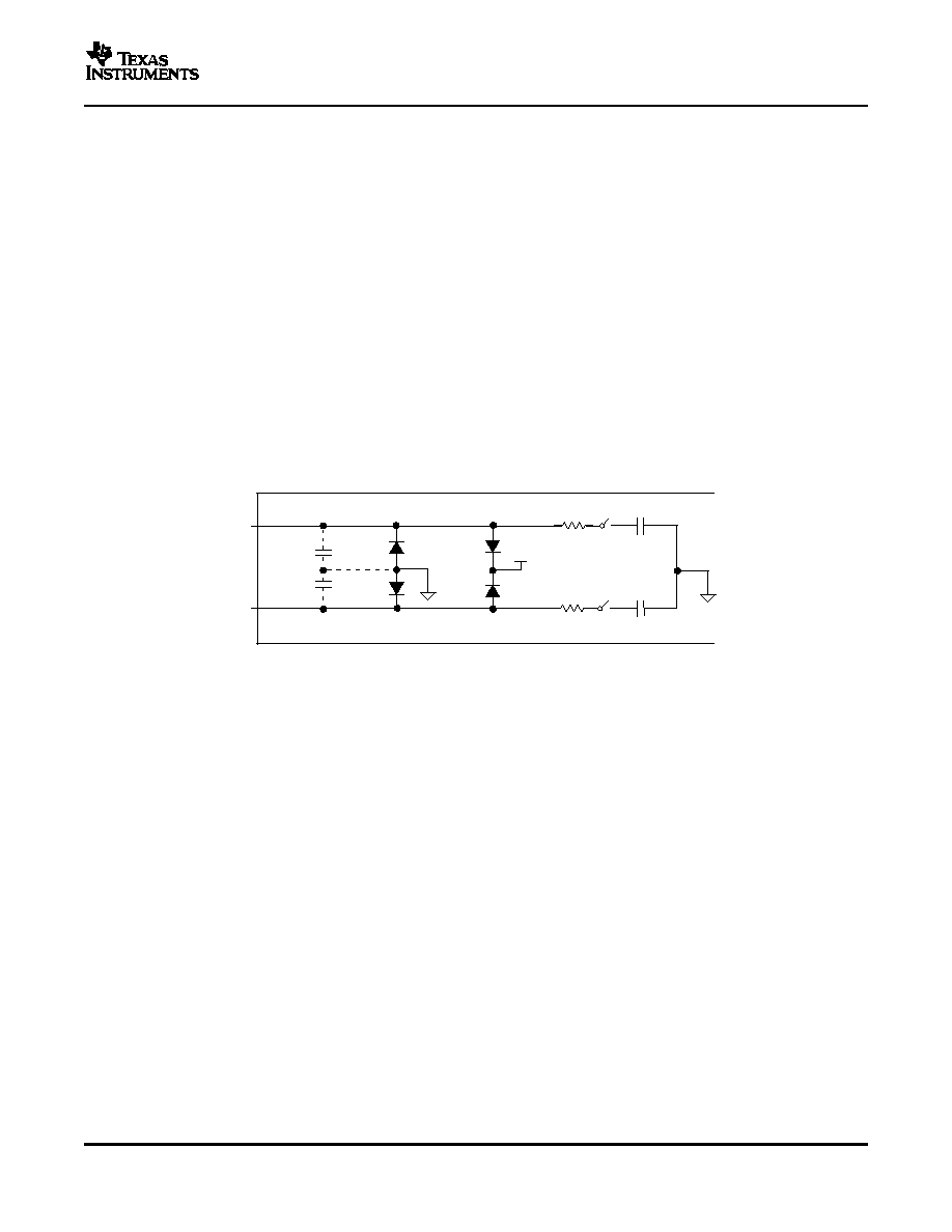
THEORY OF OPERATION (continued)
When the converter enters hold mode, the voltage difference between the +IN and -IN inputs is captured on the
internal capacitor array. The voltage on the -IN input is limited between AGND - 0.2 V and AGND + 0.2 V,
allowing the input to reject small signals which are common to both the +IN and -IN inputs. The +IN input has a
range of -0.2 V to V
ref
+ 0.2 V. The input span (+IN - (-IN)) is limited to 0 V to V
ref
.
The (peak) input current through the analog inputs depends upon a number of factors: sample rate, input
voltage, and source impedance. The current into the ADS8327/28 charges the internal capacitor array during the
sample period. After this capacitance has been fully charged, there is no further input current. The source of the
analog input voltage must be able to charge the input capacitance (45 pF) to a 16-bit settling level within the
minimum acquisition time (238 ns). When the converter goes into hold mode, the input impedance is greater
than 1 G
.
Care must be taken regarding the absolute analog input voltage. To maintain linearity of the converter, the +IN
and -IN inputs and the span (+IN - (-IN)) should be within the limits specified. Outside of these ranges, converter
linearity may not meet specifications. To minimize noise, low bandwidth input signals with low-pass filters should
be used. Care should be taken to ensure that the output impedance of the sources driving the +IN and -IN
inputs are matched. If this is not observed, the two inputs could have different settling times. This may result in
an offset error, gain error, and linearity error which change with temperature and input voltage.
Figure 51. Input Equivalent Circuit
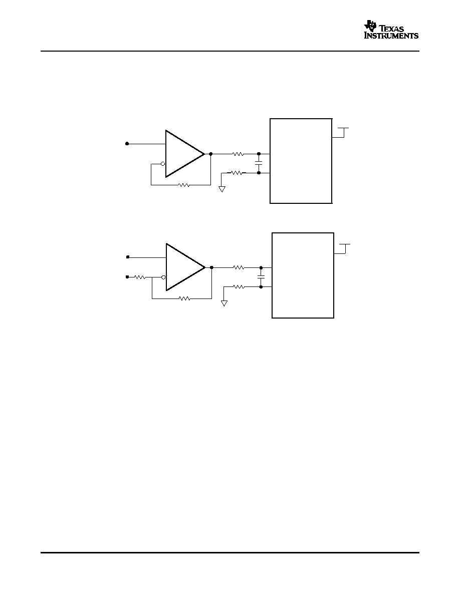
The analog input to the converter needs to be driven with a low noise, op-amp like the THS4031 or OPA356. An
RC filter is recommended at the input pins to low-pass filter the noise from the source. Two resistors of 20
and
a capacitor of 470 pF is recommended. The input to the converter is a unipolar input voltage in the range 0 V to
V
ref
. The minimum -3dB bandwidth of the driving operational amplifier can be calculated to:
f
3db
= (ln(2) ◊(n+1))/(2
◊ t
ACQ
)
where n is equal to 16, the resolution of the ADC (in the case of the ADS8327/28). When t
ACQ
= 238 ns
(minimum acquisition time), the minimum bandwidth of the driving amplifier is 7.9 MHz. The bandwidth can be
relaxed if the acquisition time is increased by the application. The OPA365, OPA827, or THS4031 from Texas
Instruments are recommended. The THS4031 used in the source follower configuration to drive the converter is
shown in the typical input drive configuration,
Figure 52
.
In systems where the input is bipolar, the THS4031 can be used in the inverting configuration with an additional
DC bias applied to its + input so as to keep the input to the ADS8327/28 within its rated operating voltage range.
This configuration is also recommended when the ADS8327/28 is used in signal processing applications where
good SNR and THD performance is required. The DC bias can be derived from the REF3225 or the REF3240
reference voltage ICs. The input configuration shown in
Figure 53
is capable of delivering better than 91-dB
SNR and -96-dB THD at an input frequency of 10 kHz. In case bandpass filters are used to filter the input, care
should be taken to ensure that the signal swing at the input of the bandpass filter is small so as to keep the
21
Submit Documentation Feedback
www.ti.com
ADS8327/28
+IN/(+IN1 or +IN0)
-IN/COM
THS4031
20
W
20
W
470 pF
50
W
Input
Signal
(0 V to 4 V)
5 V
+VA
ADS8327
+IN/(+IN1 or +IN0)
-IN/COM
THS4031
20
W
20
W
600
W
1 V DC
600
W
Input
Signal
(-2V to 2 V)
5 V
+VA
470 pF
REFERENCE
CONVERTER OPERATION
ADS8327
ADS8328
SLAS415A ≠ APRIL 2006 ≠ REVISED MAY 2006
THEORY OF OPERATION (continued)
distortion introduced by the filter minimal. In such cases, the gain of the circuit shown in
Figure 53
can be
increased to keep the input to the ADS8327/28 large to keep the SNR of the system high. Note that the gain of
the system from the + input to the output of the THS4031 in such a configuration is a function of the gain of the
AC signal. A resistor divider can be used to scale the output of the REF3225 or REF3240 to reduce the voltage
at the DC input to THS4031 to keep the voltage at the input of the converter within its rated operating range.
Figure 52. Unipolar Input Drive Configuration
Figure 53. Bipolar Input Drive Configuration
The ADS8327/28 can operate with an external reference with a range from 0.3 V to 4.2 V. A clean, low noise,
well-decoupled reference voltage on this pin is required to ensure good performance of the converter. A low
noise band-gap reference like the REF3240 can be used to drive this pin. A 10-
µ
F ceramic decoupling capacitor
is required between the REF+ and REF- pins of the converter. These capacitors should be placed as close as
possible to the pins of the device. The REF- should be connected to its own via to the analog ground plane with
the shortest possible distance.
The ADS8327/28 has an oscillator that is used as an internal clock which controls the conversion rate. The
frequency of this clock is 10.5 MHz minimum. The oscillator is always on unless the device is in the deep
powerdown state or the device is programmed for using SCLK as the conversion clock (CCLK). The minimum
acquisition (sampling) time takes 3 CCLKs (this is equivalent to 238 ns at 12.6 MHz) and the conversion time
takes 18 conversion clocks (CCLK) (~1500 ns) to complete one conversion.
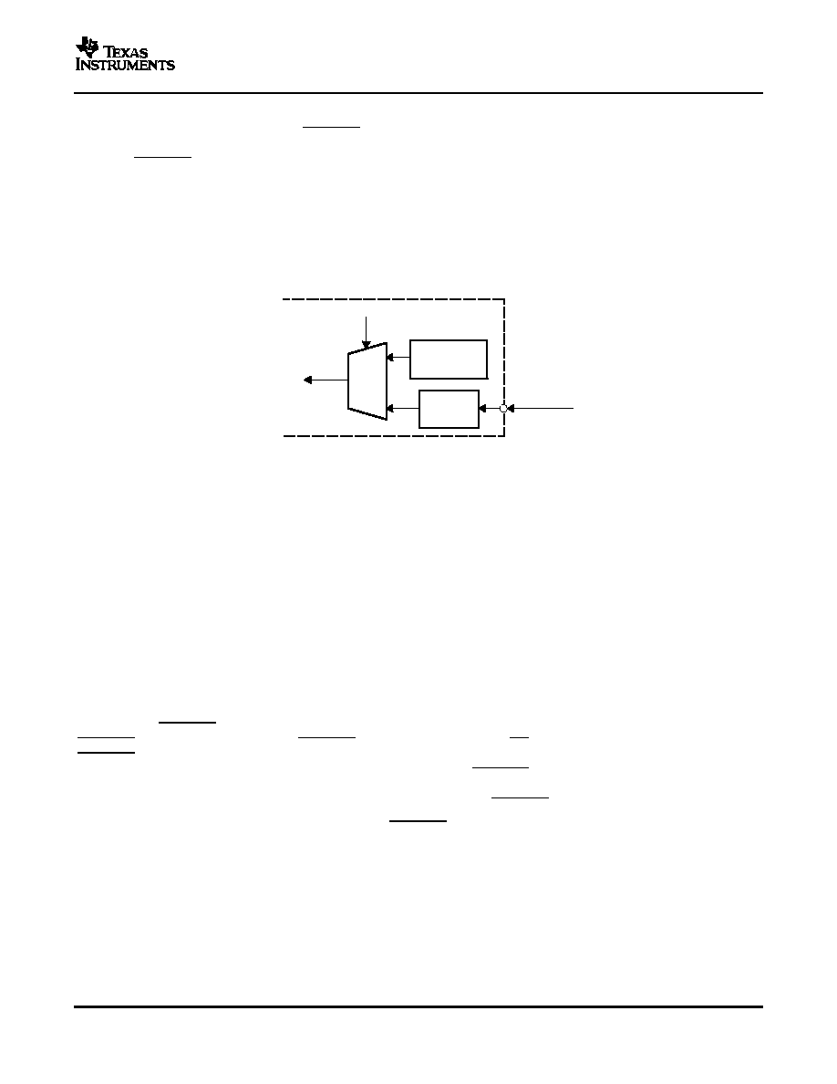
The conversion can also be programmed to run based on the external serial clock, SCLK, if is so desired. This
allows a system designer to achieve system synchronization. The serial clock SCLK, is first reduced to 1/2 of its
frequency before it is used as the conversion clock (CCLK). For example, with a 21-MHz SCLK this provides a
10.5-MHz clock for conversions. If it is desired to start a conversion at a specific rising edge of the SCLK when
the external SCLK is programmed as the source of the conversion clock (CCLK) (and manual start of conversion
22
Submit Documentation Feedback
www.ti.com
OSC
Divider
1/2
= 1
= 0
Conversion Clock
(CCLK)
CFR_D10
SPI Serial
Clock (SCLK)
Manual Channel Select Mode
Auto Channel Select Mode
Start of a Conversion
ADS8327
ADS8328
SLAS415A ≠ APRIL 2006 ≠ REVISED MAY 2006
THEORY OF OPERATION (continued)
is selected), the setup time between CONVST and that rising SCLK edge should be observed. This ensures the
conversion is complete in 18 CCLKs (or 36 SCLKs). The minimum setup time is 20 ns to ensure synchronization
between CONVST and SCLK. In many cases the conversion can start one SCLK period (or CCLK) later which
results in a 19 CCLK (or 37 SCLK) conversion. The 20 ns setup time is not required once synchronization is
relaxed.
The duty cycle of SCLK is not critical as long as it meets the minimum high and low time requirements of 8 ns.
Since the ADS8327/28 is designed for high-speed applications, a higher serial clock (SCLK) must be supplied to
be able to sustain the high throughput with the serial interface and so the clock period of SCLK must be at most
1
µ
s (when used as conversion clock (CCLK). The minimum clock frequency is also governed by the parasitic
leakage of the capacitive digital-to-analog (CDAC) capacitors internal to the ADS8327/28.
Figure 54. Converter Clock
The conversion cycle starts with selecting an acquisition channel by writing a channel number to the command
register (CMR). This cycle time can be as short as 4 serial clocks (SCLK).
Channel selection can also be done automatically if auto channel select mode is enabled. This is the default
channel select mode. The dual channel converter, ADS8328, has a built-in 2-to-1 MUX. If the device is
programmed for auto channel select mode then signals from channel 0 and channel 1 are acquired with a fixed
order. Channel 0 is accessed first in the next cycle after the command cycle that configured CFR_D11 to 1 for
auto channel select mode. This automatic access stops the cycle after the command cycle that sets CFR_D11
to 0.
The end of acquisition or sampling instance (EOS) is the same as the start of a conversion. This is initiated by
bringing the CONVST pin low for a minimum of 40 ns. After the minimum requirement has been met, the
CONVST pin can be brought high. CONVST acts independent of FS/CS so it is possible to use one common
CONVST for applications requiring simultaneous sample/hold with multiple converters. The ADS8327/28
switches from sample to hold mode on the falling edge of the CONVST signal. The ADS8327/28 requires 18
conversion clock (CCLK) edges to complete a conversion. The conversion time is equivalent to 1500 ns with a
12-MHz internal clock. The minimum time between two consecutive CONVST signals is 21 CCLKs.
A conversion can also be initiated without using CONVST if it is so programmed (CFR_D9 = 0). When the
converter is configured as auto trigger, the next conversion is automatically started 3 conversion clocks (CCLK)
after the end of a conversion. These 3 conversion clocks (CCLK) are used as the acquisition time. In this case
the time to complete one acquisition and conversion cycle is 21 CCLKs.
23
Submit Documentation Feedback
www.ti.com
Status Output EOC/INT
Power-Down Modes
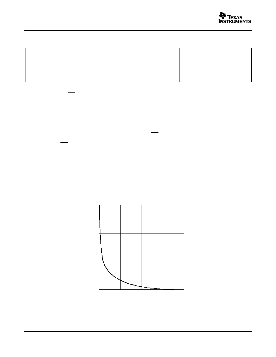
0.1
1
10
100
20
10020
20020
30020
40020
Settling Time - ns
+V
A - Supply Current -
m
A
ADS8327
ADS8328
SLAS415A ≠ APRIL 2006 ≠ REVISED MAY 2006
THEORY OF OPERATION (continued)
Table 1. Different Types of Conversion
MODE
SELECT CHANNEL
START CONVERSION
Auto Channel Select
(1)
Auto Trigger
Automatic No need to write channel number to the CMR. Use internal sequencer for the
Start a conversion based on the
ADS8328.
conversion clock CCLK.
Manual Channel Select
Manual Trigger
Manual
Write the channel number to the CMR.
Start a conversion with CONVST.
(1)
Auto channel select should be used with auto trigger and also with the TAG bit enabled.
When the status pin is programmed as EOC and the polarity is set as active low, the pin works in the following
manner: The EOC output goes LOW immediately following CONVST going LOW when manual trigger is
programmed. EOC stays LOW throughout the conversion process and returns to HIGH when the conversion has
ended. The EOC output goes low for 3 conversion clocks (CCLK) after the previous rising edge of EOC, if auto
trigger is programmed.
This status pin is programmable. It can be used as an EOC output (CFR.D[7:6] = 1, 1) where the low time is
equal to the conversion time. This status pin can be used as INT. (CFR.D[7:6] = 1, 0) which is set LOW at the
end of a conversion is brought to HIGH (cleared) by the next read cycle. The polarity of this pin, used as either
function (EOC or INT), is programmable through CFR_D7.
The ADS8327/28 has a comprehensive built-in power-down feature. There are three power-down modes: Deep
power-down mode, Nap power-down mode, and auto nap power-down mode. All three power-down modes are
enabled by setting the related CFR bits. The first two power-down modes are activated when enabled. A wakeup
command, 1011b, can resume device operation from a power-down mode. Auto nap power-down mode works
slightly different. When the converter is enabled in auto nap power-down mode, an end of conversion instance
(EOC) puts the device into auto nap powerdown. The beginning of sampling resumes operation of the converter.
The contents of the configuration register is not affected by any of the power-down modes. Any ongoing
conversion when nap or deep powerdown is activated is aborted.
Figure 55. Typical Analog Supply Current Drop vs Time After Powerdown
24
Submit Documentation Feedback
www.ti.com
ADS8327
ADS8328
SLAS415A ≠ APRIL 2006 ≠ REVISED MAY 2006
Deep Power-Down Mode
Deep power-down mode can be activated by writing to configuration register bit CFR_D2. When the device is in
deep power-down mode, all blocks except the interface are in powerdown. The external SCLK is blocked to the
analog block. The analog blocks no longer have bias currents and the internal oscillator is turned off. In this
mode, power dissipation falls from 5 mA to 1
µ
A in 2
µ
s. The wake-up time after a powerdown is 1
µ
s. When bit
D2 in the configuration register is set to 0, the device is in deep powerdown. Setting this bit to 1 or sending a
wake-up command can resume the converter from the deep power-down state.
Nap Mode
In nap mode the ADS8327/28 turns off biasing of the comparator and the mid-volt buffer. In this mode power
dissipation falls from 5 mA in normal mode to about 0.3 mA in 200 ns after the configuration cycle. The wake-up
(resume) time from nap power-down mode is 3 CCLKs (238 ns with a 12.6-MHz conversion clock). As soon as
the CFR_D3 bit in the control register is set to 0, the device goes into nap power-down mode, regardless of the
conversion state. Setting this bit to 1 or sending a wake-up command can resume the converter from the nap
power-down state.
Auto Nap Mode
Auto nap mode is almost identical to nap mode. The only difference is the time when the device is actually
powered down and the method to wake up the device. Configuration register bit D4 is only used to
enable/disable auto nap mode. If auto nap mode is enabled, the device turns off biasing after the conversion has
finished, which means the end of conversion activates auto nap powerdown mode. Power dissipation falls from
12 mA in normal mode to about 0.3 mA in 200 ns. A wake-up command resumes the device and turns biasing
on again in 3 CCLKs (238 ns with a 12.6-MHz conversion clock). The device can also be woken up by disabling
auto nap mode when bit D4 of the configuration register is set to 1. Any channel select command 0XXXb or the
set default mode command 1111b can also wake up the device from auto nap powerdown.
NOTE:
1. This wake-up command is the word 1011b in the command word. This command sets bits
D2 and D3 to 1 in the configuration register but not D4. But a wake-up command does
remove the device from either one of these power-down states, deep/nap/auto nap
powerdown.
2. Wake-up time is defined as the time between when the host processor tries to wake up
the converter and when a convert start can occur.
Table 2. Power-Down Mode Comparisons
TYPE OF
POWER
ACTIVATED BY
ACTIVATION TIME
RESUME POWER BY
RESUME TIME
ENABLE
POWERDOWN
CONSUMPTION
Normal operation
5 mA/3.8 mA
Deep powerdown
6 nA/2 nA
Setting CFR
100
µ
s
Woken up by command 1011b
1
µ
s
Set CFR
Woken up by command 1011b to achieve 6.6 mA
Nap powerdown
0.3 mA/0.2 mA
Setting CFR
200
µ
s
3 CCLKs
Set CFR
since (1.3 + 12)/2 = 6.6
Woken up by CONVST, any channel select
EOC (end of
Auto nap powerdown
200
µ
s
command, default command 1111b, or wake up
3 CCLKs
Set CFR
conversion)
command 1011b.
25
Submit Documentation Feedback
www.ti.com
N
N+1
Converter
State
EOC
EOS
EOS
EOC
Read N-1 -th Result
Read N -th Result
N -th Conversion
N+1 -th Conversion
N+1 -th Sampling
20 ns MIN
Converter State
0 ns MIN
CS
CS
CONVST
Read While Converting
Read While Sampling
(For Read Result)
(For Read Result)
20 ns MIN
1 CCLK MIN
N
N+1
Manual Trigger
Converter
State
EOC
EOS
EOC
EOS
Read N-1 -th
Result
20 ns MIN
Read N -th
Result
20 ns MIN
Read N-1 -th
Result
20 ns MIN
Read N -th
Result
20 ns MIN
Resume
Activation
N -th Sampling
>=3CCLK
N -th Conversion
=18 CCLK
Resume
Activation
N+1 -th Sampling
>=3CCLK
N+1 -th Conversion
=18 CCLK
CS
CS
CONVST
Read While Converting
Read While Sampling
0 ns MIN
1 CCLK MIN
20 ns MIN
20 ns MIN
20 ns MIN
20 ns MIN
ADS8327
ADS8328
SLAS415A ≠ APRIL 2006 ≠ REVISED MAY 2006
Figure 56. Read While Converting vs Read While Sampling (Manual trigger)
Figure 57. Read While Converting vs Read While Sampling with Deep or Nap Powerdown
26
Submit Documentation Feedback
www.ti.com
N
N+1
Manual Trigger Case 1
EOS
EOC
EOS
EOC
(programmed
Active Low)
Converter
State
Resume
N -th Sampling
>=3CCLK
EOC
EOS
N -th Conversion
=18 CCLK
Resume
N+1 -th Sampling
>=3CCLK
EOC
EOS
N+1 -th Conversion
=18 CCLK
Read N-1 -th
Result
20 ns MIN
Read N -th
Result
20 ns MIN
Read N-1 -th
Result
1 CCLK MIN
Read N -th
Result
1 CCLK MIN
Converter
State
Resume
N -th Sampling
>=3CCLK
EOC
N -th Conversion
=18 CCLK
Resume
N+1 -th Sampling
>=3CCLK
N+1 -th Conversion
=18 CCLK
Read N-1 -th
Result
20 ns MIN
Read N -th
Result
20 ns MIN
Read N-1 -th
Result
20 ns MIN
Read N -th
Result
20 ns MIN
40 ns MIN
EOC
(programmed
Active Low)
N
N+1
40 ns MIN
POWERDOWN
POWERDOWN
CONVST
CS
Read While Converting
0 ns MIN
CONVST
CS
Read While Sampling
POWER
DOWN
POWER
DOWN
CS
Read While Converting
Read While Sampling
CS
0 ns MIN
Manual Trigger Case 2 (wake up by CONVST)
6 CCLKs
6 CCLKs
20 ns MIN
20 ns MIN
20 ns MIN
20 ns MIN
20 ns MIN
20 ns MIN
20 ns MIN
20 ns MIN
ADS8327
ADS8328
SLAS415A ≠ APRIL 2006 ≠ REVISED MAY 2006
Figure 58. Read While Converting vs Read While Sampling with Auto Nap Powerdown
Total Acquisition + Conversion Cycle Time:
Automatic:
= 21 CCLKs
Manual:
21 CCLKs
Manual + deep powerdown:
4SCLK + 100
µ
s + 3 CCLK + 18 CCLK +16 SCLK + 1
µ
s
Manual + nap powerdown:
4 SCLK + 3 CCLK + 3 CCLK + 18 CCLK +16 SCLK
Manual + auto nap
4 SCLK + 3 CCLK + 3 CCLK + 18 CCLK +16 SCLK (use wakeup to resume)
powerdown:
Manual + auto nap
1 CCLK + 3 CCLK + 3 CCLK + 18 CCLK +16 SCLK (use CONVST to resume)
powerdown:
27
Submit Documentation Feedback

www.ti.com
DIGITAL INTERFACE
Internal Register
WRITING TO THE CONVERTER
ADS8327
ADS8328
SLAS415A ≠ APRIL 2006 ≠ REVISED MAY 2006
The serial interface is compatible with Motorola SPI. The serial clock is designed to accommodate the latest
high-speed processors with an SCLK up to 50 MHz. Each cycle is started with the falling edge of FS/CS. The
internal data register content which is made available to the output register at the EOC is presented on the SDO
output pin at the falling edge of FS/CS. This is the MSB. Output data are changed at the falling edge of SCLK so
that the host processor can read it at the next rising edge. Serial data input is latched at the falling edge of
SCLK.
The complete serial I/O cycle starts with the first rising edge of SCLK after the falling edge of FS/CS and ends
16 (see NOTE) falling edges of SCLK later. The serial interface is very flexible. It works with both CPOL = 0 or
CPOL = 1. The interface ignores data if a falling edge arrives before the first rising edge. This means the falling
edge of FS/CS may fall while SCLK is high. The same relaxation applies to the rising edge of FS/CS where
SCLK may be high or low as long as the last SCLK falling edge happens before the rising edge of FS/CS.
NOTE:
There are cases where a cycle is 4 SCLKs or up to 24 SCLKs depending on the read
mode combination. See
Table 3
for details.
The internal register consists of two parts, 4 bits for the command register (CMR) and 12 bits for configuration
data register (CFR).
Table 3. Command Set Defined by Command Register (CMR)
(1)
WAKE UP FROM
MINIMUM SCLKs
D[15:12]
HEX
COMMAND
D[11:0]
R/W
AUTO NAP
REQUIRED
0000b
0h
Select analog input channel 0
(2)
Don't care
Y
4
≠
0001b
1h
Select analog input channel 1
(2)
Don't care
Y
4
≠
0010b
2h
Reserved
Reserved
Y
4
≠
0011b
3h
Reserved
Reserved
Y
4
≠
0100b
4h
Reserved
Reserved
Y
4
≠
0101b
5h
Reserved
Reserved
Y
4
≠
0110b
6h
Reserved
Reserved
Y
4
≠
0111b
7h
Reserved
Reserved
Y
4
≠
1000b
8h
Reserved
Reserved
≠
≠
≠
1001b
9h
Reserved
Reserved
≠
≠
≠
1010b
Ah
Reserved
Reserved
≠
≠
≠
1011b
Bh
Wake up
Don't care
Y
4
W
1100b
Ch
Read CFR
Don't care
≠
16
R
1101b
Dh
Read data
Don't care
≠
16
R
1110
Eh
Write CFR
CFR Value
≠
16
W
1111b
Fh
Default mode (load CFR with default value)
Don't care
Y
4
W
(1)
When SDO is not in 3-state (FS/CS low and SCLK running), the bits from SDO are always part (depending on how many SCLKs are
supplied) of the previous conversion result.
(2)
These two commands apply to the ADS8328 only.
There are two different types of writes to the register, a 4-bit write to the CMR and a full 16-bit write to the CMR
plus CFR. The command set is listed in
Table 3
. A simple command requires only 4 SCLKs and the write takes
effect at the 4th falling edge of SCLK. A 16-bit write or read takes at least 16 SCLKs (see
Table 5
for exceptions
that require more than 16 SCLKs).
28
Submit Documentation Feedback
www.ti.com
Configuring the Converter and Default Mode
READING THE CONFIGURATION REGISTER
READING CONVERSION RESULT
ADS8327
ADS8328
SLAS415A ≠ APRIL 2006 ≠ REVISED MAY 2006
The converter can be configuring with command 1110b (write to the CFR) or command 1111b (default mode). A
write to the CFR requires a 4-bit command followed by 12-bits of data. A 4-bit command takes effect at the 4th
falling edge of SCLK. A CFR write takes effect at the 16th falling edge of SCLK.
A default mode command can be achieved by simply tying SDI to +VBD. As soon as the chip is selected at least
four 1s are clocked in by SCLK. The default value of the CFR is loaded into the CFR at the 4th falling edge of
SCLK.
CFR default values are all 1s (except for CFR_D1, this bit is ignored by the ADS8327 and is always read as a
0). The same default values apply for the CFR after a power-on reset (POR) and SW reset.
The host processor can read back the value programmed in the CFR by issuing command 1100b. The timing is
similar to reading a conversion result except CONVST is not used and there is no activity on the EOC/INT pin.
The CFR value read back contains the first four MSBs of conversion data plus valid 12-bit CFR contents.
Table 4. Configuration Register (CFR) Map
SDI BIT
DEFINITION
CFR - D[11 - 0]
Channel select mode
D11 Default = 1
0: Manual channel select enabled. Use channel select commands to
1: Auto channel select enabled. All channels are sampled and
access a different channel.
converted sequentially until the cycle after this bit is set to 0.
Conversion clock (CCLK) source select
D10 Default = 1
0: Conversion clock (CCLK) = SCLK/2
1: Conversion clock (CCLK) = Internal OSC
Trigger (conversion start) select: start conversion at the end of sampling (EOS). If D9 = 0, the D4 setting is ignored.
D9 Default = 1
0: Auto trigger automatically starts (4 internal clocks after EOC inactive)
1: Manual trigger manually started by falling edge of CONVST
D8 Default = 1
Don't care
Don't care
Pin 10 polarity select when used as an output (EOC/INT)
D7 Default = 1
0: EOC Active high / INT active high
1: EOC Active low / INT active low
Pin 10 function select when used as an output (EOC/INT)
D6 Default = 1
0: Pin used as INT
1: Pin used as EOC
Pin 10 I/O select for chain mode operation
D5 Default = 1
0: Pin 10 is used as CDI input (chain mode enabled)
1: Pin 10 is used as EOC/INT output
Auto nap powerdown enable/disable (mid voltage and comparator shut down between cycles). This bit setting is ignored if D9 = 0.
D4 Default = 1
0: Auto nap powerdown enabled (not activated)
1: Auto nap powerdown disabled
Nap powerdown (mid voltage and comparator shut down between cycles). This bit is set to 1 automatically by wake-up command.
D3 Default = 1
0: Enable/activate device in nap powerdown
1: Remove device from nap powerdown (resume)
Deep powerdown. This bit is set to 1 automatically by wake-up command.
D2 Default = 1
0: Enable/activate device in deep powerdown
1: Remove device from deep powerdown (resume)
D1 Default =
TAG bit enable. This bit is ignored by the ADS8327 and is alway read 0.
0: ADS8327
0: TAG bit disabled.
1: TAG bit output enabled. TAG bit appears at the 17th SCLK.
1: ADS8328
Reset
D0 Default = 1
0: System reset
1: Normal operation
The conversion result is available to the input of the output data register (ODR) at EOC and presented to the
output of the output register at the next falling edge of CS or FS. The host processor can then shift the data out
via the SDO pin any time except during the quiet zone. This is 20 ns before and 20 ns after the end of sampling
(EOS) period. End of sampling (EOS) is defined as the falling edge of CONVST when manual trigger is used or
the end of the 3rd conversion clock (CCLK) after EOC if auto trigger is used.
29
Submit Documentation Feedback
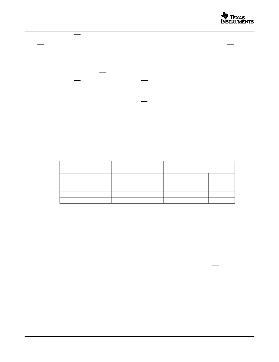
www.ti.com
TAG Mode
Chain Mode
ADS8327
ADS8328
SLAS415A ≠ APRIL 2006 ≠ REVISED MAY 2006
The falling edge of FS/CS should not be placed at the precise moment (minimum of at least one conversion
clock (CCLK) delay) at the end of a conversion (by default when EOC goes high), otherwise the data is corrupt.
If FS/CS is placed before the end of a conversion, the previous conversion result is read. If FS/CS is placed
after the end of a conversion, the current conversion result is read.
The conversion result is 16-bit data in straight binary format as shown in
Table 4
. Generally 16 SCLKs are
necessary, but there are exceptions where more than 16 SCLKS are required (see
Table 5
). Data output from
the serial output (SDO) is left adjusted MSB first. The trailing bits are filled with the TAG bit first (if enabled) plus
all zeros. SDO remains low until FS/CS is brought high again.
SDO is active when FS/CS is low. The rising edge of FS/CS 3-states the SDO output.
NOTE:
Whenever SDO is not in 3-state (when FS/CS is low and SCLK is running), a portion
of the conversion result is output at the SDO pin. The number of bits depends on how
many SCLKs are supplied. For example, a manual select channel command cycle
requires 4 SCLKs, therefore 4 MSBs of the conversion result are output at SDO. The
exception is SDO outputs all 1s during the cycle immediately after any reset (POR or
software reset).
If SCLK is used as the conversion clock (CCLK) and a continuous SCLK is used, it is not possible to clock out
all 16 SDO bits during the sampling time (6 SCLKs) because of the quiet zone requirement. In this case it is
better to read the conversion result during the conversion time (36 SCLKs or 48 SCLKs in auto nap mode).
Table 5. Ideal Input Voltages and Output Codes
DESCRIPTION
ANALOG VALUE
DIGITAL OUTPUT
Full scale range
V
ref
STRAIGHT BINARY
Least significant bit (LSB)
V
ref
/65536
BINARY CODE
HEX CODE
Full scale
+V
ref
≠ 1 LSB
1111 1111 1111 1111
FFFF
Midscale
V
ref
/2
1000 0000 0000 0000
8000
Midscale ≠ 1 LSB
V
ref
/2≠ 1 LSB
0111 1111 1111 1111
7FFF
Zero
0 V
0000 0000 0000 0000
0000
The ADS8328 includes a feature, TAG, that can be used as a tag to indicate which channel sourced the
converted result. An address bit is added after the LSB read out from SDO indicating which channel the result
came from if TAG mode is enabled. This address bit is 0 for channel 0 and 1 for channel 1. The converter
requires more than the 16 SCLKs that are required for a 4 bit command plus 12 bit CFR or 16 data bits because
of the additional TAG bit.
The ADS8327/28 can operate as a single converter or in a system with multiple converters. System designers
can take advantage of the simple high-speed SPI compatible serial interface by cascading them in a single chain
when multiple converters are used. A bit in the CFR is used to reconfigure the EOC/INT status pin as a
secondary serial data input, chain data input (CDI), for the conversion result from an upstream converter. This is
chain mode operation. A typical connection of three converters is shown in
Figure 59
.
30
Submit Documentation Feedback
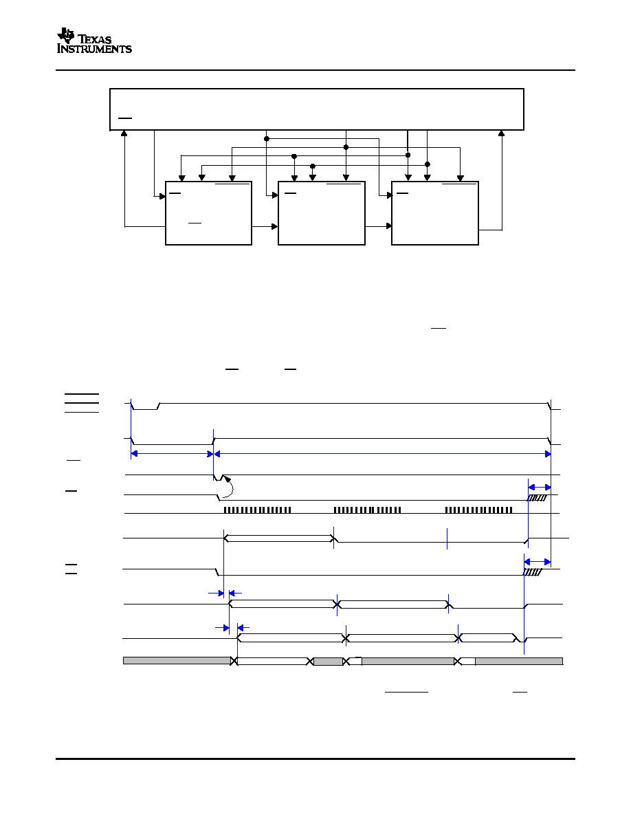
www.ti.com
ADS8327
#1
SDI
SDO
ADS8327
#2
SDI
SDO
ADS8327
#3
SDI
SDO
Micro Controller
SDI
SDO
GPIO1
GPIO2
GPIO3
Program device #1 CFR_D[7:5] = XX0b
INT
CS
CONVST
CS
CONVST
CS
CONVST
EOC/INT
CDI
CDI
Program device #2 and #3 CFR_D[7:5] = XX1b
SCLK
SCLK
SCLK
SCLK
CONVST #1,
CONVST
CONVST
#2,
#3
EOC #1
(active low)
INT #3
(active low)
CS/FS #2,
/FS #3
CS
SCLK #1,
SCLK #2,
SCLK #3
SDO #1,
CDI #2
SDO #2,
CDI #3
SDO #3
SDI #1,
SDI #2,
SDI #3
CONFIGURE
READ Result
READ Result
EOS
EOC
EOS
Nth
Nth from #1
Nth from #1
Nth from #1
N ! 1th from #2
Nth from #3
N ! 1th from #2
Nth from #1
1110............
1101b
1101b
1 . . . . . . . . . . . . . . . . . . 16
Cascaded Manual Trigger/Read While Sampling
(Use internal CCLK, EOC active low, and
active low) held
INT
CS
low during the N times 16 bits transfer cycle.
Hi-Z
Hi-Z
Hi-Z
Hi-Z
1 . . . . . . . . . . . . . . . . . . 16
1 . . . . . . . . . . . . . . . . . . 16
Hi-Z
Hi-Z
CS/FS #1
t
CONV
= 18 CCLKs
t
d(SDO-CDI)
t
SAMPLE1
= 3 CCLKs min
t
d(CSR-EOS)
= 20 ns min
t
d(CSR-EOS)
= 20 ns min
t
d(SDO-CDI)
ADS8327
ADS8328
SLAS415A ≠ APRIL 2006 ≠ REVISED MAY 2006
Figure 59. Multiple Converters Connected Using Chain Mode
When multiple converters are used in chain mode, the first converter is configured in regular mode while the rest
of the converters downstream are configured in chain mode. When a converter is configured in chain mode, the
CDI input data goes straight to the output register, therefore the serial input data passes through the converter
with a 16 SCLK (if the TAG feature is disabled) or a 24 SCLK delay, as long as CS is active. See
Figure 60
for
detailed timing. In this timing the conversion in each converters are done simultaneously.
Figure 60. Simplified Cascade Mode Timing with Shared CONVST and Continuous CS
31
Submit Documentation Feedback
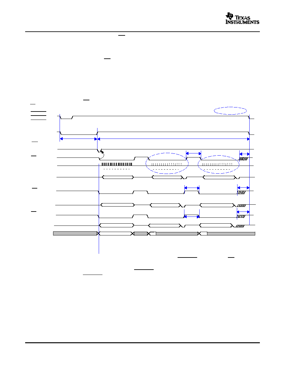
www.ti.com
These SCLKs are optional.
CONFIGURE
READ Result
READ Result
EOS
EOC
EOS
Nth
Nth from #1
Nth from #1
Nth from #1
Nth from #1
Nth from #1
N ! 1th from #2
Nth from #3
N ! 1th from #2
Nth from #1
1110............
1101b
1101b
1
16
1
16
1
16
Cascaded Manual Trigger/Read While Sampling
(Use internal CCLK, EOC, and
polarity programmed as active low)
held low during the N times 16 bits transfer cycle.
INT
CS
CONVST #1,
CONVST
CONVST
#2,
#3
EOC #1
(active low)
INT #1
(active low)
CS/FS #3
SCLK #1,
SCLK #2,
SCLK #3
SDO #1,
CDI #2
SDO #2,
CDI #3
SDO #3
SDI #1,
SDI #2,
SDI #3
CS/FS #1
CS/FS #2
SCLK #2,
t
CONV
= 18 CCLKs
t
SAMPLE1
= 3 CCLKs min
t
=
20 ns min
d(EOS-CSF)
t
d(EOS-CSF)
=
20 ns min
t
d(CSR-EOS)
= 20 ns min
t
=
20 ns min
d(CSR-EOS)
t
d(CSR-EOS)
=
20 ns min
t
d(EOS-CSF)
= 20 ns min
ADS8327
ADS8328
SLAS415A ≠ APRIL 2006 ≠ REVISED MAY 2006
Care must be given to handle the multiple CS signals when the converters are operating in chain mode. The
different chip select signals must be low for the entire data transfer (in this example 48 bits for three converters).
The first 16-bit word after the falling chip select is always the data from the chip that received the chip select
signal.
Case 1: If chip select is not toggled (CS stays low), the next 16 bits are data from the upstream converter, and
so on. This is shown in
Figure 60
. If there is no upstream converter in the chain, as converter #1 in the example,
the same data from the converter is going to be shown repeatedly.
Case 2: If the chip select is toggled during a chain mode data transfer cycle, as illustrated in
Figure 61
, the
same data from the converter is read out again and again in all three discrete 16-bit cycles. This is not a desired
result.
Figure 61. Simplified Cascade Mode Timing with Shared CONVST and Discrete CS
Figure 62
shows a slightly different scenario where CONVST is not shared by the second converter. Converters
#1 and #3 have the same CONVST signal. In this case, converter #2 simply passes previous conversion data
downstream.
32
Submit Documentation Feedback
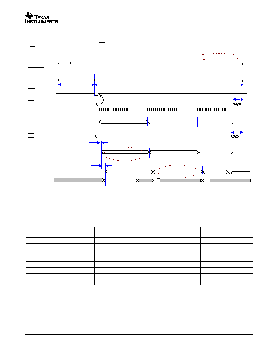
www.ti.com
Note : old data shown.
CONFIGURE
READ Result
READ Result
EOS
EOC
EOS
Nth
Nth from #1
Nth from #1
Nth from #1
N ! 1th from #2
Nth from #3
N ! 1th from #2
1110............
1101b
1101b
1 . . . . . . . . . . . . . . . . . .16
1 . . . . . . . . . . . . . . . . . .16
1 . . . . . . . . . . . . . . . . . .16
Hi-Z
Hi-Z
Hi-Z
Hi-Z
Hi-Z
Hi-Z
Cascaded Manual Trigger/Read While Sampling
(Use internal CCLK, EOC active low and
active low)
held low during the N times 16 bits transfer cycle.
INT
CS
CONVST #1,
CONVST #3
CONVST #2 = 1
EOC #1
(active low)
INT #1
(active low)
SCLK #1,
SCLK #2,
SCLK #3
SDO #1,
CDI #2
SDO #2,
CDI #3
SDO #3
SDI #1,
SDI #2,
SDI #3
CS/FS #1
CS/FS #2,
CS/FS #3
t
CONV
= 18 CCLKs
t
SAMPLE1
= 3 CCLKs min
t
d(CSR-EOS)
= 20 ns min
t
d(CSR-EOS)
= 20 ns min
t
d(SDO-CDI)
t
d(SDO-CDI)
ADS8327
ADS8328
SLAS415A ≠ APRIL 2006 ≠ REVISED MAY 2006
Figure 62. Simplified Cascade Timing (Separate CONVST)
The number of SCLKs required for a serial read cycle depends on the combination of different read modes, TAG
bit, chain mode, and the way a channel is selected, i.e., auto channel select. This is listed in
Table 6
.
Table 6. Required SCLKs For Different Read Out Mode Combinations
CHAIN MODE
AUTO CHANNEL
NUMBER OF SCLK PER SPI
TAG ENABLED CFR.D1
TRAILING BITS
ENABLED CFR.D5 SELECT CFR.D11
READ
0
0
0
16
None
0
0
1
17
MSB is TAG bit plus zero(s)
0
1
0
16
None
0
1
1
17
TAG bit plus 7 zeros
1
0
0
16
None
1
0
1
24
TAG bit plus 7 zeros
1
1
0
16
None
1
1
1
24
TAG bit plus 7 zeros
33
Submit Documentation Feedback
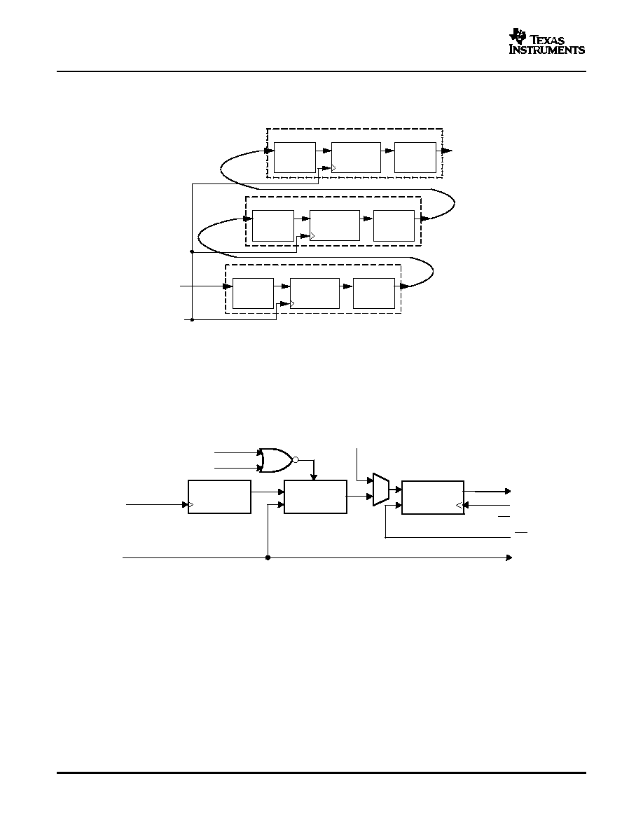
www.ti.com
Logic
Delay
< = 8 .3 ns
ADS 8327
# 3
Q
D
CLK
Logic
Delay
< = 8 .3 ns
ADS 8327
# 2
Q
D
CLK
Logic
Delay
< = 8 .3 ns
ADS 8327
# 1
Q
D
CLK
SCLK input
SDO
SDO
SDO
CDI
CDI
CDI
Serial data
input
Serial data
output
Logic
Delay
Plus PAD
2.7 ns
Logic
Delay
Plus PAD
2.7 ns
Logic
Delay
Plus PAD
8.3 ns
Logic
Delay
Plus PAD
8.3 ns
Logic
Delay
Plus PAD
2.7 ns
Logic
Delay
Plus PAD
8.3 ns
RESET
Intermediate
Latch
SAR Shift
Register
Output
Register
Conversion Clock
SW RESET
POR
SET
Latched by Falling Edge of CS
Latched by End Of
Conversion
EOC
SDO
SCLK
CS
EOC
CDI
ADS8327
ADS8328
SLAS415A ≠ APRIL 2006 ≠ REVISED MAY 2006
SCLK skew between converters and data path delay through the converters configured in chain mode can affect
the maximum frequency of SCLK. The delay can also be affected by supply voltage and loading. It may be
necessary to slow down the SCLK when the devices are configured in chain mode.
Figure 63. Typical Delay Through Converters Configured in Chain Mode
The converter has two reset mechanisms, a power-on reset (POR) and a software reset using CFR_D0. These
two mechanisms are NOR-ed internally. When a reset (software or POR) is issued, all register data are set to
the default values (all 1s) and the SDO output (during the cycle immediately after reset) is set to all 1s. The state
machine is reset to the power-on state.
Figure 64. Digital Output Under Reset Condition
34
Submit Documentation Feedback
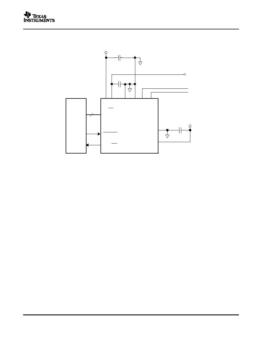
www.ti.com
APPLICATION INFORMATION
TYPICAL CONNECTION
Host
Processor
FS/CS
SDO
SDI
SCLK
CONVST
EOC/INT
4.7
m
F
+VA REF+
AGND IN+ IN-
4.7
m
F
Analog +5 V
Interface
Supply
+1.8 V
BDGND
+VBD
Analog Input
ADS8327
REF-
10
m
F
Ext Ref Input
AGND
AGND
ADS8327
ADS8328
SLAS415A ≠ APRIL 2006 ≠ REVISED MAY 2006
Figure 65. Typical Circuit Configuration
35
Submit Documentation Feedback
PACKAGING INFORMATION
Orderable Device
Status
(1)
Package
Type
Package
Drawing
Pins Package
Qty
Eco Plan
(2)
Lead/Ball Finish
MSL Peak Temp
(3)
ADS8327IBPW
ACTIVE
TSSOP
PW
16
90
Green (RoHS &
no Sb/Br)
CU NIPDAU
Level-2-260C-1 YEAR
ADS8327IBPWG4
ACTIVE
TSSOP
PW
16
90
Green (RoHS &
no Sb/Br)
CU NIPDAU
Level-2-260C-1 YEAR
ADS8327IBPWR
ACTIVE
TSSOP
PW
16
2000 Green (RoHS &
no Sb/Br)
CU NIPDAU
Level-2-260C-1 YEAR
ADS8327IBPWRG4
ACTIVE
TSSOP
PW
16
2000 Green (RoHS &
no Sb/Br)
CU NIPDAU
Level-2-260C-1 YEAR
ADS8327IBRSAR
PREVIEW
QFN
RSA
16
3000
TBD
Call TI
Call TI
ADS8327IBRSAT
PREVIEW
QFN
RSA
16
250
TBD
Call TI
Call TI
ADS8327IPW
ACTIVE
TSSOP
PW
16
90
Green (RoHS &
no Sb/Br)
CU NIPDAU
Level-2-260C-1 YEAR
ADS8327IPWG4
ACTIVE
TSSOP
PW
16
90
Green (RoHS &
no Sb/Br)
CU NIPDAU
Level-2-260C-1 YEAR
ADS8327IPWR
ACTIVE
TSSOP
PW
16
2000 Green (RoHS &
no Sb/Br)
CU NIPDAU
Level-2-260C-1 YEAR
ADS8327IPWRG4
ACTIVE
TSSOP
PW
16
2000 Green (RoHS &
no Sb/Br)
CU NIPDAU
Level-2-260C-1 YEAR
ADS8327IRSAR
PREVIEW
QFN
RSA
16
3000
TBD
Call TI
Call TI
ADS8327IRSAT
PREVIEW
QFN
RSA
16
250
TBD
Call TI
Call TI
ADS8328IBPW
ACTIVE
TSSOP
PW
16
90
Green (RoHS &
no Sb/Br)
CU NIPDAU
Level-2-260C-1 YEAR
ADS8328IBPWG4
ACTIVE
TSSOP
PW
16
90
Green (RoHS &
no Sb/Br)
CU NIPDAU
Level-2-260C-1 YEAR
ADS8328IBPWR
ACTIVE
TSSOP
PW
16
2000 Green (RoHS &
no Sb/Br)
CU NIPDAU
Level-2-260C-1 YEAR
ADS8328IBPWRG4
ACTIVE
TSSOP
PW
16
2000 Green (RoHS &
no Sb/Br)
CU NIPDAU
Level-2-260C-1 YEAR
ADS8328IBRSAR
PREVIEW
QFN
RSA
16
3000
TBD
Call TI
Call TI
ADS8328IBRSAT
PREVIEW
QFN
RSA
16
250
TBD
Call TI
Call TI
ADS8328IPW
ACTIVE
TSSOP
PW
16
90
Green (RoHS &
no Sb/Br)
CU NIPDAU
Level-2-260C-1 YEAR
ADS8328IPWG4
ACTIVE
TSSOP
PW
16
90
Green (RoHS &
no Sb/Br)
CU NIPDAU
Level-2-260C-1 YEAR
ADS8328IPWR
ACTIVE
TSSOP
PW
16
2000 Green (RoHS &
no Sb/Br)
CU NIPDAU
Level-2-260C-1 YEAR
ADS8328IPWRG4
ACTIVE
TSSOP
PW
16
2000 Green (RoHS &
no Sb/Br)
CU NIPDAU
Level-2-260C-1 YEAR
ADS8328IRSAR
PREVIEW
QFN
RSA
16
3000
TBD
Call TI
Call TI
ADS8328IRSAT
PREVIEW
QFN
RSA
16
250
TBD
Call TI
Call TI
(1)
The marketing status values are defined as follows:
ACTIVE: Product device recommended for new designs.
LIFEBUY: TI has announced that the device will be discontinued, and a lifetime-buy period is in effect.
NRND: Not recommended for new designs. Device is in production to support existing customers, but TI does not recommend using this part in
a new design.
PREVIEW: Device has been announced but is not in production. Samples may or may not be available.
OBSOLETE: TI has discontinued the production of the device.
PACKAGE OPTION ADDENDUM
www.ti.com
12-Sep-2006
Addendum-Page 1

(2)
Eco Plan - The planned eco-friendly classification: Pb-Free (RoHS), Pb-Free (RoHS Exempt), or Green (RoHS & no Sb/Br) - please check
http://www.ti.com/productcontent
for the latest availability information and additional product content details.
TBD: The Pb-Free/Green conversion plan has not been defined.
Pb-Free (RoHS): TI's terms "Lead-Free" or "Pb-Free" mean semiconductor products that are compatible with the current RoHS requirements
for all 6 substances, including the requirement that lead not exceed 0.1% by weight in homogeneous materials. Where designed to be soldered
at high temperatures, TI Pb-Free products are suitable for use in specified lead-free processes.
Pb-Free (RoHS Exempt): This component has a RoHS exemption for either 1) lead-based flip-chip solder bumps used between the die and
package, or 2) lead-based die adhesive used between the die and leadframe. The component is otherwise considered Pb-Free (RoHS
compatible) as defined above.
Green (RoHS & no Sb/Br): TI defines "Green" to mean Pb-Free (RoHS compatible), and free of Bromine (Br) and Antimony (Sb) based flame
retardants (Br or Sb do not exceed 0.1% by weight in homogeneous material)
(3)
MSL, Peak Temp. -- The Moisture Sensitivity Level rating according to the JEDEC industry standard classifications, and peak solder
temperature.
Important Information and Disclaimer:The information provided on this page represents TI's knowledge and belief as of the date that it is
provided. TI bases its knowledge and belief on information provided by third parties, and makes no representation or warranty as to the
accuracy of such information. Efforts are underway to better integrate information from third parties. TI has taken and continues to take
reasonable steps to provide representative and accurate information but may not have conducted destructive testing or chemical analysis on
incoming materials and chemicals. TI and TI suppliers consider certain information to be proprietary, and thus CAS numbers and other limited
information may not be available for release.
In no event shall TI's liability arising out of such information exceed the total purchase price of the TI part(s) at issue in this document sold by TI
to Customer on an annual basis.
PACKAGE OPTION ADDENDUM
www.ti.com
12-Sep-2006
Addendum-Page 2
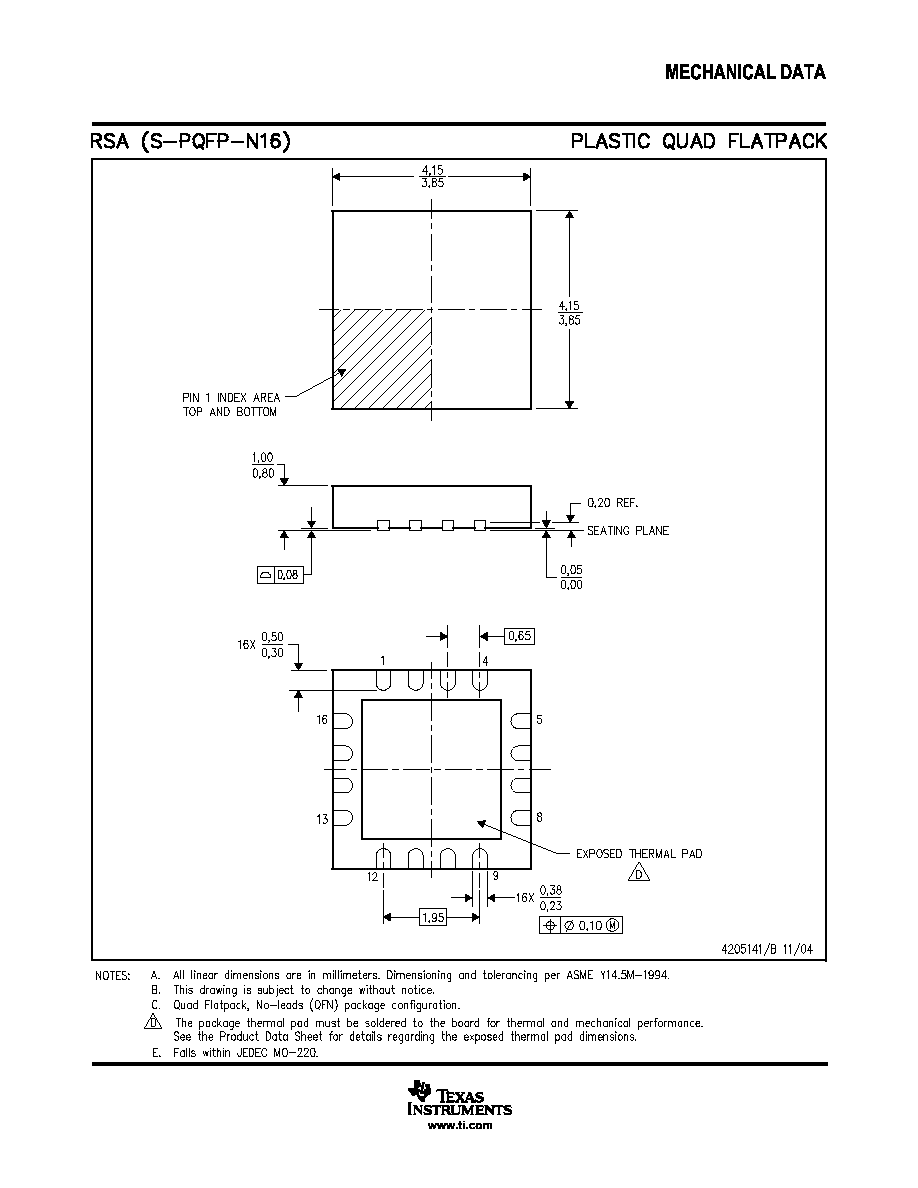
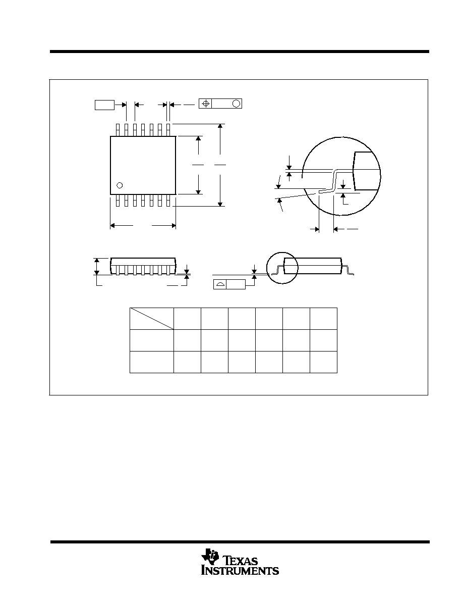
MECHANICAL DATA
MTSS001C ≠ JANUARY 1995 ≠ REVISED FEBRUARY 1999
POST OFFICE BOX 655303
∑
DALLAS, TEXAS 75265
PW (R-PDSO-G**)
PLASTIC SMALL-OUTLINE PACKAGE
14 PINS SHOWN
0,65
M
0,10
0,10
0,25
0,50
0,75
0,15 NOM
Gage Plane
28
9,80
9,60
24
7,90
7,70
20
16
6,60
6,40
4040064/F 01/97
0,30
6,60
6,20
8
0,19
4,30
4,50
7
0,15
14
A
1
1,20 MAX
14
5,10
4,90
8
3,10
2,90
A MAX
A MIN
DIM
PINS **
0,05
4,90
5,10
Seating Plane
0
∞
≠ 8
∞
NOTES: A. All linear dimensions are in millimeters.
B. This drawing is subject to change without notice.
C. Body dimensions do not include mold flash or protrusion not to exceed 0,15.
D. Falls within JEDEC MO-153

IMPORTANT NOTICE
Texas Instruments Incorporated and its subsidiaries (TI) reserve the right to make corrections, modifications,
enhancements, improvements, and other changes to its products and services at any time and to discontinue
any product or service without notice. Customers should obtain the latest relevant information before placing
orders and should verify that such information is current and complete. All products are sold subject to TI's terms
and conditions of sale supplied at the time of order acknowledgment.
TI warrants performance of its hardware products to the specifications applicable at the time of sale in
accordance with TI's standard warranty. Testing and other quality control techniques are used to the extent TI
deems necessary to support this warranty. Except where mandated by government requirements, testing of all
parameters of each product is not necessarily performed.
TI assumes no liability for applications assistance or customer product design. Customers are responsible for
their products and applications using TI components. To minimize the risks associated with customer products
and applications, customers should provide adequate design and operating safeguards.
TI does not warrant or represent that any license, either express or implied, is granted under any TI patent right,
copyright, mask work right, or other TI intellectual property right relating to any combination, machine, or process
in which TI products or services are used. Information published by TI regarding third-party products or services
does not constitute a license from TI to use such products or services or a warranty or endorsement thereof.
Use of such information may require a license from a third party under the patents or other intellectual property
of the third party, or a license from TI under the patents or other intellectual property of TI.
Reproduction of information in TI data books or data sheets is permissible only if reproduction is without
alteration and is accompanied by all associated warranties, conditions, limitations, and notices. Reproduction
of this information with alteration is an unfair and deceptive business practice. TI is not responsible or liable for
such altered documentation.
Resale of TI products or services with statements different from or beyond the parameters stated by TI for that
product or service voids all express and any implied warranties for the associated TI product or service and
is an unfair and deceptive business practice. TI is not responsible or liable for any such statements.
Following are URLs where you can obtain information on other Texas Instruments products and application
solutions:
Products
Applications
Amplifiers
amplifier.ti.com
Audio
www.ti.com/audio
Data Converters
dataconverter.ti.com
Automotive
www.ti.com/automotive
DSP
dsp.ti.com
Broadband
www.ti.com/broadband
Interface
interface.ti.com
Digital Control
www.ti.com/digitalcontrol
Logic
logic.ti.com
Military
www.ti.com/military
Power Mgmt
power.ti.com
Optical Networking
www.ti.com/opticalnetwork
Microcontrollers
microcontroller.ti.com
Security
www.ti.com/security
Low Power Wireless www.ti.com/lpw
Telephony
www.ti.com/telephony
Video & Imaging
www.ti.com/video
Wireless
www.ti.com/wireless
Mailing Address:
Texas Instruments
Post Office Box 655303 Dallas, Texas 75265
Copyright
2006, Texas Instruments Incorporated