 | –≠–ª–µ–∫—Ç—Ä–æ–Ω–Ω—ã–π –∫–æ–º–ø–æ–Ω–µ–Ω—Ç: ADS8343 | –°–∫–∞—á–∞—Ç—å:  PDF PDF  ZIP ZIP |
Document Outline
- FEATURES
- APPLICATIONS
- DESCRIPTION
- PACKAGE/ORDERING INFORMATION
- ABSOLUTE MAXIMUM RATINGS
- PIN CONFIGURATIONS
- PIN DESCRIPTIONS
- ELECTRICAL CHARACTERISTICS: +5V
- ELECTRICAL CHARACTERISTICS: +2.7V
- TYPICAL CHARACTERISTICS: +5V
- TYPICAL CHARACTERISTICS: +2.7V
- THEORY OF OPERATION
- ANALOG INPUT
- REFERENCE INPUT
- DIGITAL INTERFACE
- Control Byte
- Clock Modes
- External Clock Mode
- Internal Clock Mode
- Digital Timing
- DATA FORMAT
- POWER DISSIPATION
- NOISE
- AVERAGING
- LAYOUT
- PACKAGE DRAWING
- DBQ (R-PDSO-G**) PLASTIC SMALL-OUTLINE
- IMPORTANT NOTICE
ADS8343
16-Bit, 4-Channel Serial Output Sampling
ANALOG-TO-DIGITAL CONVERTER
FEATURES
q
BIPOLAR INPUT RANGE
q
PIN-FOR-PIN COMPATIBLE WITH THE
ADS7841 AND ADS8341
q
SINGLE SUPPLY: 2.7V to 5V
q
4-CHANNEL SINGLE-ENDED OR
2-CHANNEL DIFFERENTIAL INPUT
q
UP TO 100kHz CONVERSION RATE
q
86dB SINAD
q
SERIAL INTERFACE
q
SSOP-16 PACKAGE
DESCRIPTION
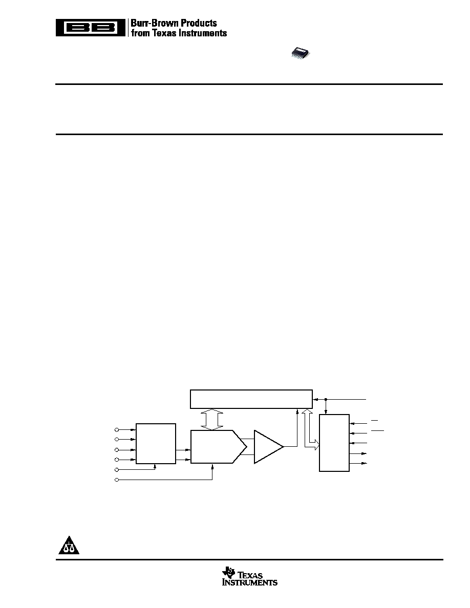
The ADS8343 is a 4-channel, 16-bit sampling Analog-to-
Digital (A/D) converter with a synchronous serial interface.
Typical power dissipation is 8mW at a 100kHz throughput
rate and a +5V supply. The reference voltage (V
REF
) can be
varied between 500mV and V
CC
/2, providing a corresponding
input voltage range of
±
V
REF
. The device includes a shut-
down mode which reduces power dissipation to under 15
µ
W.
The ADS8343 is ensured down to 2.7V operation.
Low power, high speed, and an onboard multiplexer make
the ADS8343 ideal for battery-operated systems such as
personal digital assistants, portable multi-channel data log-
gers, and measurement equipment. The serial interface also
provides low-cost isolation for remote data acquisition. The
ADS8343 is available in an SSOP-16 package and is en-
sured over the ≠40
∞
C to +85
∞
C temperature range.
APPLICATIONS
q
DATA ACQUISITION
q
TEST AND MEASUREMENT
q
INDUSTRIAL PROCESS CONTROL
q
PERSONAL DIGITAL ASSISTANTS
q
BATTERY-POWERED SYSTEMS
CDAC
SAR
Comparator
Four
Channel
Multiplexer
Serial
Interface
and
Control
CH0
CH1
CH2
CH3
COM
V
REF
CS
SHDN
DIN
DOUT
BUSY
DCLK
ADS8
343
www.ti.com
Copyright © 2001, Texas Instruments Incorporated
Please be aware that an important notice concerning availability, standard warranty, and use in critical applications of
Texas Instruments semiconductor products and disclaimers thereto appears at the end of this data sheet.
SBAS183A ≠ JANUARY 2001 ≠ REVISED OCTOBER 2002
PRODUCTION DATA information is current as of publication date.
Products conform to specifications per the terms of Texas Instruments
standard warranty. Production processing does not necessarily include
testing of all parameters.
ADS8343
2
SBAS183A
www.ti.com
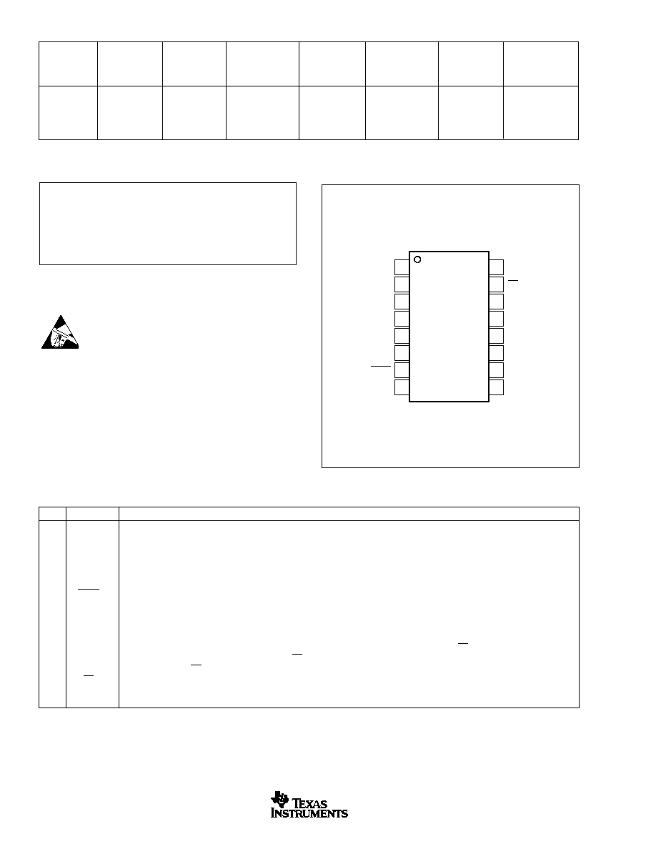
PIN CONFIGURATIONS
Top View
SSOP
PIN DESCRIPTIONS
PIN
NAME
DESCRIPTION
1
+V
CC
Power Supply, 2.7V to 5V
2
CH0
Analog Input Channel 0
3
CH1
Analog Input Channel 1
4
CH2
Analog Input Channel 2
5
CH3
Analog Input Channel 3
6
COM
Common reference for analog inputs. This pin is typically connected to V
REF
.
7
SHDN
Shutdown. When LOW, the device enters a very low power shutdown mode.
8
V
REF
Voltage Reference Input. See Electrical Characteristic Table for ranges.
9
+V
CC
Power Supply, 2.7V to 5V
10
GND
Ground
11
GND
Ground
12
DOUT
Serial Data Output. Data is shifted on the falling edge of DCLK. This output is high impedance when CS is HIGH.
13
BUSY
Busy Output. This output is high impedance when CS is HIGH.
14
DIN
Serial Data Input. If CS is LOW, data is latched on rising edge of DCLK.
15
CS
Chip Select Input. Controls conversion timing and enables the serial input/output register.
16
DCLK
External Clock Input. This clock runs the SAR conversion process and synchronizes serial data I/O. Maximum input clock frequency
equals 2.4MHz to achieve 100kHz sampling rate.
ABSOLUTE MAXIMUM RATINGS
(1)
+V
CC
to GND ........................................................................ ≠0.3V to +6V
Analog Inputs to GND ............................................ ≠0.3V to +V
CC
+ 0.3V
Digital Inputs to GND ........................................................... ≠0.3V to +6V
Power Dissipation .......................................................................... 250mW
Maximum Junction Temperature ................................................... +150
∞
C
Operating Temperature Range ........................................ ≠40
∞
C to +85
∞
C
Storage Temperature Range ......................................... ≠65
∞
C to +150
∞
C
Lead Temperature (soldering, 10s) ............................................... +300
∞
C
NOTE: (1) Stresses above those listed under "Absolute Maximum Ratings"
may cause permanent damage to the device. Exposure to absolute maximum
conditions for extended periods may affect device reliability.
1
2
3
4
5
6
7
8
+V
CC
CH0
CH1
CH2
CH3
COM
SHDN
V
REF
DCLK
CS
DIN
BUSY
DOUT
GND
GND
+V
CC
16
15
14
13
12
11
10
9
ADS8343
ELECTROSTATIC
DISCHARGE SENSITIVITY
This integrated circuit can be damaged by ESD. Texas Instru-
ments recommends that all integrated circuits be handled with
appropriate precautions. Failure to observe proper handling
and installation procedures can cause damage.
ESD damage can range from subtle performance degrada-
tion to complete device failure. Precision integrated circuits
may be more susceptible to damage because very small
parametric changes could cause the device not to meet its
published specifications.
PACKAGE/ORDERING INFORMATION
MAXIMUM
NO
INTEGRAL
MISSING
SPECIFIED
LINEARITY
CODES
PACKAGE
TEMPERATURE
ORDERING
TRANSPORT
PRODUCT
ERROR (LSB)
ERROR (LSB)
PACKAGE-LEAD
DESIGNATOR
(1)
RANGE
NUMBER
MEDIA, QUANTITY
ADS8343E
8
14
SSOP-16
DBQ
≠40
∞
C to +85
∞
C
ADS8343E
Rails, 100
"
"
"
"
"
"
ADS8343E/2K5
Tape and Reel, 2500
ADS8343EB
6
15
SSOP-16
DBQ
≠40
∞
C to +85
∞
C
ADS8343EB
Rails, 100
"
"
"
"
"
"
ADS8343EB/2K5
Tape and Reel, 2500
NOTE: (1) For the most current specifications and package information, refer to our web site at www.ti.com.
ADS8343
3
SBAS183A
www.ti.com
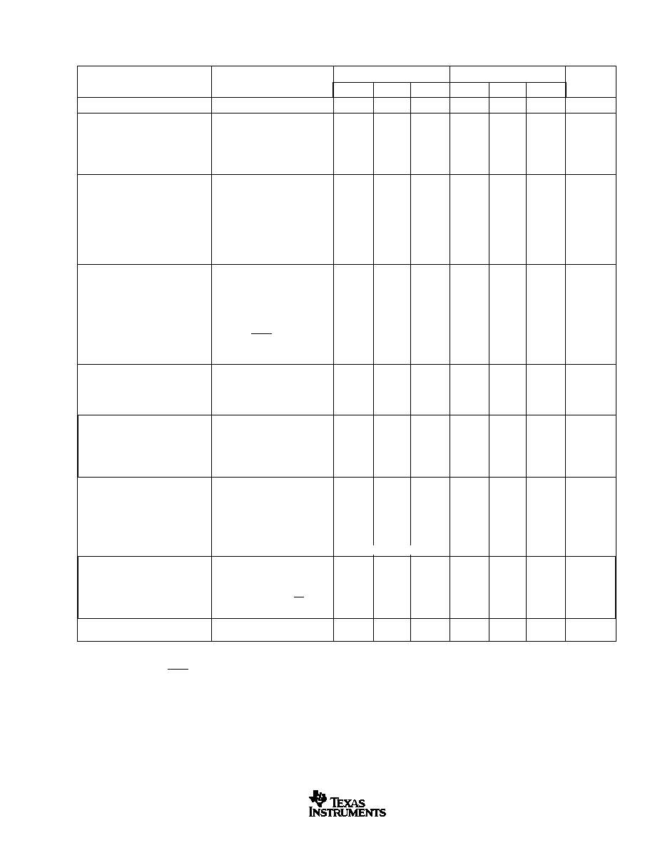
ELECTRICAL CHARACTERISTICS: +5V
At T
A
= ≠40
∞
C to +85
∞
C, +V
CC
= +5V, V
REF
= +2.5V, f
SAMPLE
= 100kHz, and f
CLK
= 24 ∑ f
SAMPLE
= 2.4MHz, unless otherwise noted.
ADS8343E
ADS8343EB
Same specifications as ADS8343E.
NOTES: (1) LSB means Least Significant Bit. With V
REF
equal to +2.5V, one LSB is 76
µ
V. (2) First nine harmonics of the test frequency. (3) Auto power-down mode
(PD1 = PD0 = 0) active or SHDN = GND. (4) Power-down after conversion mode with external clock gated `HIGH'.
PARAMETER
CONDITIONS
MIN
TYP
MAX
MIN
TYP
MAX
UNITS
RESOLUTION
16
Bits
ANALOG INPUT
Full-Scale Input Span
Positive Input-Negative Input
≠V
REF
+V
REF
V
Absolute Input Range
Positive Input
≠0.2
+V
CC
+ 0.2
V
Negative Input
≠0.2
+V
CC
+ 0.2
V
Capacitance
25
pF
Leakage Current
±
1
µ
A
SYSTEM PERFORMANCE
No Missing Codes
14
15
Bits
Integral Linearity Error
±
8
±
6
LSB
Bipolar Error
±
2
±
1
mV
Bipolar Error Match
2.3
8.0
LSB
(1)
Gain Error
±
0.05
±
0.024
%
Gain Error Match
1.0
4.0
LSB
Noise
20
µ
Vrms
Power-Supply Rejection
+4.75V < V
CC
< 5.25V
3
LSB
(1)
SAMPLING DYNAMICS
Conversion Time
16
Clk Cycles
Acquisition Time
4.5
Clk Cycles
Throughput Rate
100
kHz
Multiplexer Settling Time
500
ns
Aperture Delay
30
ns
Aperture Jitter
100
ps
Internal Clock Frequency
SHDN = V
DD
2.4
MHz
External Clock Frequency
0.024
2.4
MHz
Data Transfer Only
0
2.4
MHz
DYNAMIC CHARACTERISTICS
Total Harmonic Distortion
(2)
V
IN
= 5Vp-p at 10kHz
≠95
dB
Signal-to-(Noise + Distortion)
V
IN
= 5Vp-p at 10kHz
86
dB
Spurious-Free Dynamic Range
V
IN
= 5Vp-p at 10kHz
97
dB
Channel-to-Channel Isolation
V
IN
= 5Vp-p at 50kHz
100
dB
REFERENCE INPUT
Range
0.5
+V
CC
/2
V
Resistance
DCLK Static
5
G
Input Current
40
100
µ
A
f
SAMPLE
= 12.5kHz
2.5
µ
A
DCLK Static
0.001
3
µ
A
DIGITAL INPUT/OUTPUT
Logic Family
CMOS
Logic Levels
V
IH
| I
IH
|
+5
µ
A
3.0
5.5
V
V
IL
| I
IL
|
+5
µ
A
≠0.3
+0.8
V
V
OH
I
OH
= ≠250
µ
A
3.5
V
V
OL
I
OL
= 250
µ
A
0.4
V
Data Format
Binary Two's Complement
POWER-SUPPLY REQUIREMENTS
+V
CC
Specified Performance
4.75
5.25
V
Quiescent Current
1.5
2.0
mA
f
SAMPLE
= 10kHz
150
µ
A
Power-Down Mode
(3, 4)
, CS = +V
CC
3
µ
A
Power Dissipation
7.5
10
mW
TEMPERATURE RANGE
Specified Performance
≠40
+85
∞
C
ADS8343
4
SBAS183A
www.ti.com
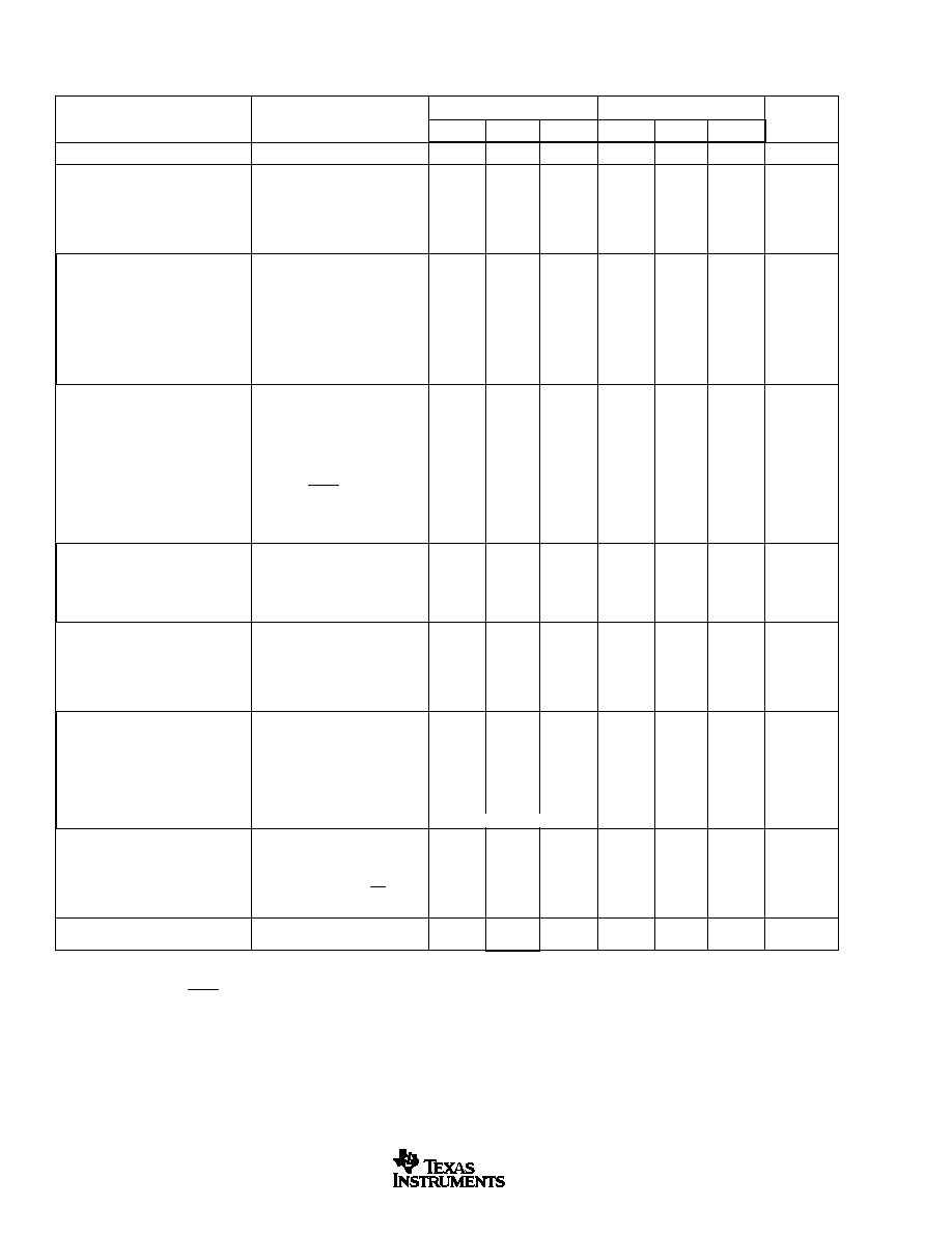
ELECTRICAL CHARACTERISTICS: +2.7V
At T
A
= ≠40
∞
C to +85
∞
C, +V
CC
= +2.7V, V
REF
= +1.25V, f
SAMPLE
= 100kHz, and f
CLK
= 24 ∑ f
SAMPLE
= 2.4MHz, unless otherwise noted.
ADS8343E
ADS8343EB
Same specifications as ADS8343E.
NOTES: (1) LSB means Least Significant Bit. With V
REF
equal to +1.25V, one LSB is 38
µ
V. (2) First nine harmonics of the test frequency. (3) Auto power-down mode
(PD1 = PD0 = 0) active or SHDN = GND. (4) Power-down after conversion mode with external clock gated `HIGH'.
PARAMETER
CONDITIONS
MIN
TYP
MAX
MIN
TYP
MAX
UNITS
RESOLUTION
16
BITS
ANALOG INPUT
Full-Scale Input Span
Positive Input-Negative Input
≠V
REF
+V
REF
V
Absolute Input Range
Positive Input
≠0.2
+V
CC
+ 0.2
V
Negative Input
≠0.2
+V
CC
+ 0.2
V
Capacitance
25
pF
Leakage Current
±
1
µ
A
SYSTEM PERFORMANCE
No Missing Codes
14
15
Bits
Integral Linearity Error
±
12
±
8
LSB
Bipolar Error
±
1
±
0.5
mV
Bipolar Error Match
1.2
4.0
LSB
Gain Error
±
0.05
±
0.0024
% of FSR
Gain Error Match
1.0
4.0
LSB
Noise
20
µ
Vrms
Power-Supply Rejection
+2.7 < V
CC
< +3.3V
3
LSB
(1)
SAMPLING DYNAMICS
Conversion Time
16
Clk Cycles
Acquisition Time
4.5
Clk Cycles
Throughput Rate
100
kHz
Multiplexer Settling Time
500
ns
Aperture Delay
30
ns
Aperture Jitter
100
ps
Internal Clock Frequency
SHDN = V
DD
2.4
MHz
External Clock Frequency
0.024
2.4
MHz
When Used with Internal Clock
0.024
2.0
MHz
Data Transfer Only
0
2.4
MHz
DYNAMIC CHARACTERISTICS
Total Harmonic Distortion
(2)
V
IN
= 2.5Vp-p at 1kHz
≠94
dB
Signal-to-(Noise + Distortion)
V
IN
= 2.5Vp-p at 1kHz
81
dB
Spurious-Free Dynamic Range
V
IN
= 2.5Vp-p at 1kHz
98
dB
Channel-to-Channel Isolation
V
IN
= 2.5Vp-p at 10kHz
100
dB
REFERENCE INPUT
Range
0.5
+V
CC
/2
V
Resistance
DCLK Static
5
G
Input Current
13
40
µ
A
f
SAMPLE
= 12.5kHz
2.5
µ
A
DCLK Static
0.001
3
µ
A
DIGITAL INPUT/OUTPUT
Logic Family
CMOS
Logic Levels
V
IH
| I
IH
|
+5
µ
A
+V
CC
∑ 0.7
5.5
V
V
IL
| I
IL
|
+5
µ
A
≠0.3
+0.8
V
V
OH
I
OH
= ≠250
µ
A
+V
CC
∑ 0.8
V
V
OL
I
OL
= 250
µ
A
0.4
V
Data Format
Binary Two's Complement
POWER-SUPPLY REQUIREMENTS
+V
CC
Specified Performance
2.7
3.6
V
Quiescent Current
1.2
1.85
mA
f
SAMPLE
= 10kHz
105
µ
A
Power-Down Mode
(3, 4)
, CS = +V
CC
3
µ
A
Power Dissipation
3.2
5
mW
TEMPERATURE RANGE
Specified Performance
≠40
+85
∞
C
ADS8343
5
SBAS183A
www.ti.com
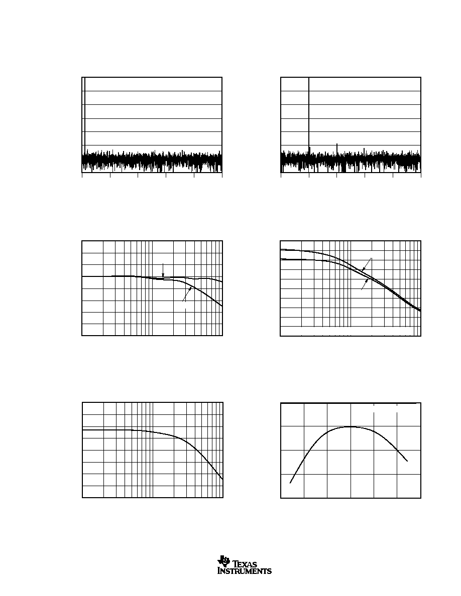
TYPICAL CHARACTERISTICS: +5V
At T
A
= +25
∞
C, +V
CC
= +5V, V
REF
= +2.5V, f
SAMPLE
= 100kHz, and f
CLK
= 24 ∑ f
SAMPLE
= 2.4MHz, unless otherwise noted.
0
≠20
≠40
≠60
≠80
≠100
≠120
≠140
FREQUENCY SPECTRUM
(4096 Point FFT; f
IN
= 1.001kHz, ≠0.2dB)
0
50
20
10
40
30
Frequency (kHz)
Amplitude (dB)
0
≠20
≠40
≠60
≠80
≠100
≠120
≠140
FREQUENCY SPECTRUM
(4096 Point FFT; f
IN
= 9.985kHz, ≠0.2dB)
0
50
20
10
40
30
Frequency (kHz)
Amplitude (dB)
SIGNAL-TO-NOISE RATIO AND
SIGNAL-TO-(NOISE + DISTORTION)
vs INPUT FREQUENCY
10
1
100
Frequency (kHz)
SNR and SINAD (dB)
100
90
80
70
60
SNR
SINAD
SPURIOUS-FREE DYNAMIC RANGE AND
TOTAL HARMONIC DISTORTION
vs INPUT FREQUENCY
10
1
100
Frequency (kHz)
SFDR (dB)
110
100
90
80
70
60
THD (dB)
≠110
≠100
≠90
≠80
≠70
≠60
SFDR
THD
(1)
NOTE: (1) First nine harmonics of the input frequency.
EFFECTIVE NUMBER OF BITS
vs INPUT FREQUENCY
10
1
100
Frequency (kHz)
Effective Number of Bits
15.0
14.5
14.0
13.5
13.0
12.5
12.0
11.5
11.0
Temperature (
∞
C)
0.1
0
≠0.1
≠0.2
≠0.3
CHANGE IN SIGNAL-TO-(NOISE + DISTORTION)
vs TEMPERATURE
25
100
≠50
≠25
0
50
75
Delta from 25
∞
C (dB)
f
IN
= 4.956kHz, ≠0.2dB