Äîêóìåíòàöèÿ è îïèñàíèÿ www.docs.chipfind.ru
PRODUCTION DATA information is current as of publication date.
Products conform to specifications per the terms of Texas Instruments
standard warranty. Production processing does not necessarily include
testing of all parameters.
ADS8361
ADS
8361
Dual, 500kSPS, 16-Bit, 2 + 2 Channel,
Simultaneous Sampling
ANALOG-TO-DIGITAL CONVERTER
FEATURES
q
2 SIMULTANEOUS 16-BIT DACs
q
4 FULLY DIFFERENTIAL INPUT CHANNELS
q
2
µ
s THROUGHPUT PER CHANNEL
q
4
µ
s TOTAL THROUGHPUT FOR FOUR CHANNELS
q
LOW POWER: 150mW
q
INTERNAL REFERENCE
q
FLEXIBLE SERIAL INTERFACE
q
16-BIT UPGRADE TO THE 12-BIT ADS7861
q
PIN COMPATIBLE WITH THE ADS7861
APPLICATIONS
q
MOTOR CONTROL
q
MULTI-AXIS POSITIONING SYSTEMS
q
3-PHASE POWER CONTROL
DESCRIPTION
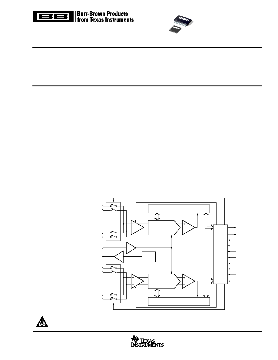
The ADS8361 is a dual, 16-bit, 500kSPS, Analog-to-Digital
(A/D) converter with four fully differential input channels grouped
into two pairs for high-speed, simultaneous signal acquisition.
Inputs to the sample-and-hold amplifiers are fully differential
and are maintained differentially to the input of the A/D con-
verter. This provides excellent common-mode rejection of
80dB at 50kHz, which is important in high-noise environments.
The ADS8361 offers a high-speed, dual serial interface and
control inputs to minimize software overhead. The output data
for each channel is available as a 16-bit word. The ADS8361
is offered in SSOP-24 and QFN-32 (5x5) packages and is fully
specified over the 40
°
C to +85
°
C operating range.
SAR
Serial
Interface
COMP
CLOCK
A0
M1
M0
CONVST
CS
RD
BUSY
SERIAL DATA B
SERIAL DATA A
CDAC
Internal
2.5V
Reference
SHA
CH A0
CH A0+
REF
IN
CH A1
CH A1+
SAR
COMP
CDAC
SHA
CH B0
CH B0+
CH B1
CH B1+
REF
OUT
ADS8361
SBAS230C AUGUST 2002 REVISED SEPTEMBER 2004
www.ti.com
Copyright © 2002-2004, Texas Instruments Incorporated
Please be aware that an important notice concerning availability, standard warranty, and use in critical applications of
Texas Instruments semiconductor products and disclaimers thereto appears at the end of this data sheet.
ADS8361
2
SBOS230C
www.ti.com
ELECTROSTATIC
DISCHARGE SENSITIVITY
This integrated circuit can be damaged by ESD. Texas Instru-
ments recommends that all integrated circuits be handled with
appropriate precautions. Failure to observe proper handling and
installation procedures can cause damage.
ESD damage can range from subtle performance degradation to
complete device failure. Precision integrated circuits may be more
susceptible to damage because very small parametric changes
could cause the device not to meet its published specifications.
MAXIMUM
INTEGRAL
NO MISSING
SPECIFIED
LINEARITY
CODES
PACKAGE
TEMPERATURE
ORDERING
TRANSPORT
PRODUCT
ERROR (LSB)
ERROR (LSB)
PACKAGE-LEAD
DESIGNATOR
(1)
RANGE
NUMBER
MEDIA, QUANTITY
ADS8361
±
8
14
SSOP-24
DBQ
40
°
C to +85
°
C
ADS8361IDBQ
Rails, 56
"
"
"
"
"
"
ADS8361IDBQR
Tape and Reel, 2500
ADS8361
±
8
14
QFN-32
RHB
40
°
C to +85
°
C
ADS8361IRHBT
Tape and Reel, 250
"
"
"
"
"
"
ADS8361IRHBR
Tape and Reel, 3000
NOTE: (1) For the most current specifications and package information, refer to our web site at www.ti.com.
PACKAGE/ORDERING INFORMATION
DERATING FACTOR
T
A
25
°
C
T
A
70
°
C
T
A
= 85
°
C
PACKAGE
R
JC
R
JA
ABOVE T
A
= 25
°
C
POWER RATING
POWER RATINGQ
POWER RATING
SSOP-24
28.5
°
C/W
88
°
C/W
11.364mW/
°
C
1420mW
909mW
738mW
QFN-32 (5x5)
1.007
°
C/W
36.7
°
C/W
27.25mW/
°
C
2725mW
1499mW
1090mW
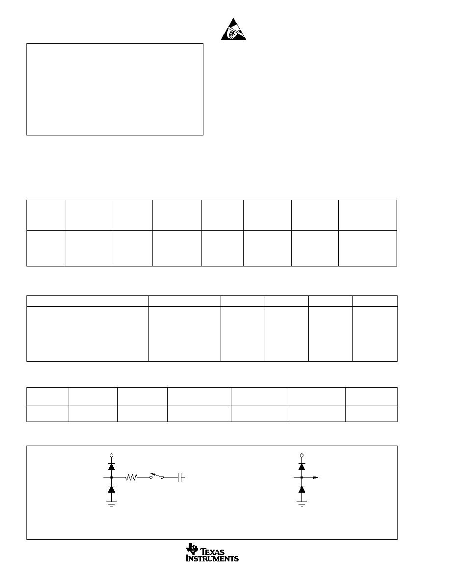
RECOMMENDED OPERATING CONDITIONS
EQUIVALENT INPUT CIRCUIT
ABSOLUTE MAXIMUM RATINGS
Absolute Maximum Ratings over operating free-air temperature (unless other-
wise noted)
(1)
.
Supply Voltage, AGND to AV
DD
............................................. 0.3V to 7V
Supply Voltage, BGND to BV
DD
............................................. 0.3V to 7V
Analog Input Voltage ................................. AGND 0.3V to AV
DD
+ 0.3V
Reference Input Voltage ........................... AGND 0.3V to AV
DD
+ 0.3V
Digital Input Voltage .................................. BGND 0.3V to BV
DD
+ 0.3V
Ground Voltage Differences, AGND to BGND ................................
±
0.3V
Voltage Differences, BV
DD
to AGND ..................................... 0.3V to 7V
Input Current to Any Pin Except Supply ......................... 20mA to 20mA
Power Dissipation ....................................... See Dissipation Rating Table
Operating Virtual Junction Temperature Range, T
J
........ 40
°
C to 150
°
C
Operating Free-Air Temperature Range, T
A
...................... 40
°
C to 85
°
C
Storage Temperature Range, T
STG
.................................. 65
°
C to 150
°
C
Lead Temperature 1.6mm (1/16 inch) from Case for 10s ...................... 260
°
C
NOTE: (1) Stresses beyond those listed under "absolute maximum ratings" may
cause permanent damage to the device. These are stress ratings only, and
functional operation of the device at these or any other conditions beyond those
indicated under "recommended operating conditions" is not implied. Exposure
to absolute-maximum-rated conditions of extended periods may affect device
reliability.
CONDITIONS
MIN
NOM
MAX
UNITS
Supply Voltage, AGND to AV
DD
4.75
5
5.25
V
Supply Voltage, BGND to BV
DD
Low-Voltage Levels
2.7
3.6
V
5V Logic Levels
4.5
5
5.5
V
Reference Input Voltage
1.2
2.5
2.6
V
Operating Common-Mode Signal
IN
2.2
2.5
2.8
V
Analog Inputs
+IN (IN)
0
±
V
REF
V
Operating Junction Temperature Range
T
J
40
105
°
C
R
ON
= 20
C
(SAMPLE)
= 25pF
BV
DD
D
IN
BGND
AV
DD
A
IN
AGND
Diode Turn on Voltage: 0.35V
Equivalent Analog Input Circuit
Equivalent Digital Input Circuit
PACKAGE DISSIPATION RATING
ADS8361
3
SBOS230C
www.ti.com
PARAMETER
CONDITIONS
MIN
TYP
(1)
MAX
UNITS
ANALOG INPUT
Full-Scale Range
(2)
(FSR)
+IN (IN)
±
V
REF
V
Operating Common-Mode Signal
2.2
2.8
V
Input Switch Resistance
IN = V
REF
20
Input Capacitance
IN = V
REF
25
pF
Input Leakage Current
IN = V
REF
±
1
nA
Differential Input Switch Resistance
40
Differential Input Capacitance
15
pF
Common-Mode Rejection Ratio
(CMRR)
At DC
84
dB
V
IN
=
±
1.25Vp-p at 50kHz
80
dB
DC ACCURACY
Resolution
16
Bits
No Missing Code
(NMC)
14
Bits
Integral Linearity Error
(INL)
±
3
±
8
LSB
(3)
Integral Linearity Match
Channel 0/1, Same A/D
4
LSB
Differential Nonlinearity
(DNL)
+1.5
(4)
LSB
Bipolar Offset Error
(V
OS
)
±
0.5
±
2
mV
Bipolar Offset Error Match
Channel 0/1, Same A/D
0.5
1
mV
Bipolar Offset Error Drift
(TCV
OS
)
0.4
ppm/
°
C
Gain Error
(6)
(G
ERR
)
±
0.05
±
0.5
%
Gain Error Match
0.05
0.15
%
Gain Error Drift
(TCG
ERR
)
20
ppm/
°
C
Noise
60
µ
Vrms
Power-Supply Rejection Ratio
(PSRR)
4.75V < AV
DD
< 5.25V, with
70
dB
External Reference, at DC
SAMPLING DYNAMICS
Conversion Time per A/D
(t
CONV
)
100kHz
f
CLK
10MHz
1.6
160
µ
s
Acquisition Time
(t
AQ
)
f
CLK
= 10MHz
400
ns
Throughout Rate
500
kSPS
Aperture Delay
5
ns
Aperture Delay Matching
100
ps
Aperture Jitter
50
ps
Clock Frequency
0.1
10
MHz
AC ACCURACY
Total Harmonic Distortion
(THD)
V
IN
=
±
2.5Vp-p at 10kHz
94
dB
Spurious-Free Dynamic Range
(SFDR)
V
IN
=
±
2.5Vp-p at 10kHz
94
dB
Signal-to-Noise Ratio
(SNR)
V
IN
=
±
2.5Vp-p at 10kHz
83
dB
Signal-to-Noise + Distortion
(SINAD)
V
IN
=
±
2.5Vp-p at 10kHz
83
dB
Channel-to-Channel Isolation
V
IN
=
±
2.5Vp-p at 10kHz
96
dB
VOLTAGE REFERENCE OUTPUT
Reference Voltage Ouput
(V
OUT
)
2.475
2.5
2.525
V
Initial Accuracy
±
1
%
Output Voltage Temperature Drift (dV
OUT
/dT)
±
20
ppm/
°
C
Output Voltage Noise
f = 0.1Hz to 10Hz, C
L
= 10
µ
F
10
µ
Vp-p
f = 10Hz to 10kHz, C
L
= 10
µ
F
12
µ
Vrms
Power-Supply Rejection Ratio
(PSRR)
60
dB
Output Current
(I
OUT
)
10
µ
A
Short-Circuit Current
(I
SC
)
0.5
mA
Turn On Settling Time
to 0.1% at C
L
= 0
100
µ
s
VOLTAGE REFERENCE INPUT
Reference Voltage Input
(V
IN
)
1.2
2.5
2.6
V
Reference Input Resistance
100
M
Reference Input Capacitance
5
pF
Reference Input Current
1
µ
A
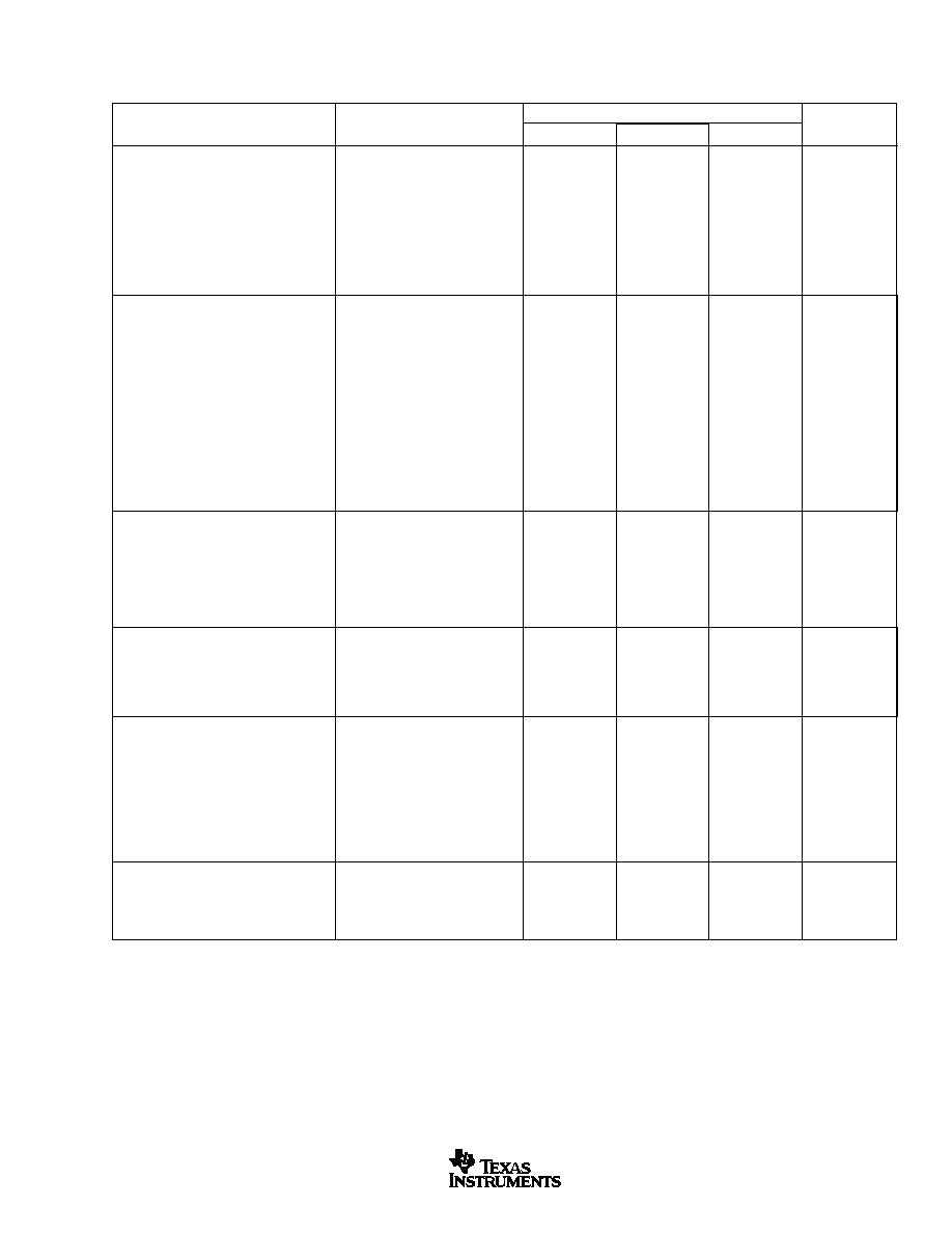
ELECTRICAL CHARACTERISTICS
Over recommended operating free-air temperature range at 40
°
C to 85
°
C, AV
DD
= 5V, BV
DD
= 3V, V
REF
= internal +2.5V, f
CLK
= 10MHz, and f
SAMPLE
= 500 kSPS,
unless otherwise noted.
NOTES: (1) All Values are at T
A
= 25
°
C. (2) Ideal input span; does not include gain or offset error. (3) LSB means Least Significant Bit, with V
REF
equal to +2.5V;
1LSB = 76
µ
V. (4) Specified for 14-bit no missing code. (5) Specified for 15-bit no missing code. (6) Measured relative to an ideal, full-scale input (+IN (IN)) of
4.9999V. Thus, gain error does not include the error of the internal voltage reference.
ADS8361
ADS8361
4
SBOS230C
www.ti.com
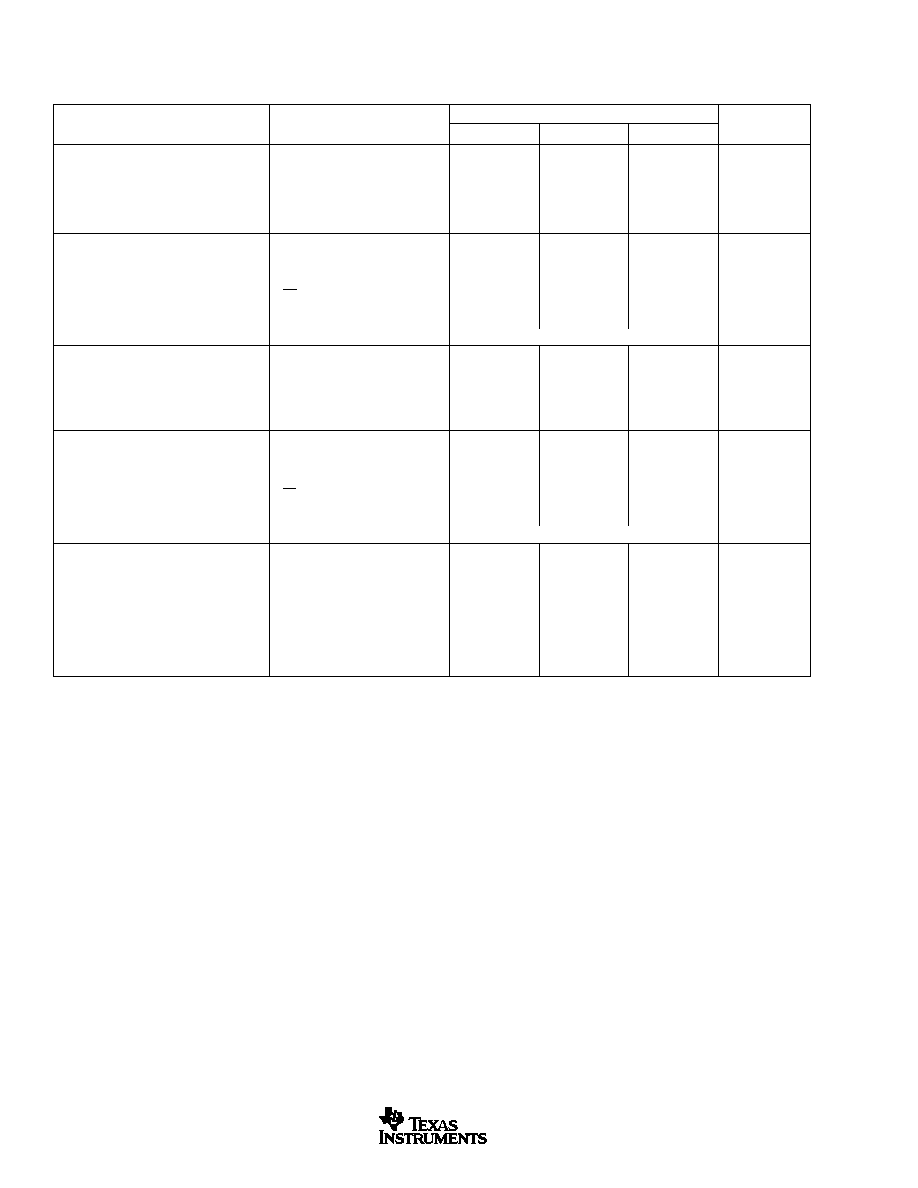
ELECTRICAL CHARACTERISTICS
Over recommended operating free-air temperature range at 40
°
C to 85
°
C, AV
DD
= 5V, V
REF
= internal +2.5V, f
CLK
= 10MHz, and f
SAMPLE
= 500 kSPS, unless otherwise
noted.
NOTES: (1) All Values are at T
A
= 25
°
C. (2) Applies for 5.0V nominal supply: BV
DD
(min) = 4.5V and BV
DD
(max) = 5.5V. (3) Applies for 3.0V nominal supply: BV
DD
(min) = 2.7V and BV
DD
(max) = 3.6V. (4) No clock active (static).
ADS8361
PARAMETER
CONDITIONS
MIN
TYP
(1)
MAX
UNITS
DIGITAL INPUTS
(2)
Logic Family
CMOS
High-Level Input Voltage
(V
IH
)
0.7 · V
DD
V
DD
+ 0.3
V
Low-Level Input Voltage
(V
IL
)
0.3
0.3 · V
DD
V
Input Current
(I
IN
)
V
I
= BV
DD
or BGND
±
50
nA
Input Capacitance
(C
I
)
5
pF
DIGITAL OUTPUTS
(2)
Logic Family
CMOS
High-Level Output Voltage
(V
OH
)
BV
DD
= 4.5V, I
OH
= 100
µ
A
4.44
V
Low-Level Output Voltage
(V
OL
)
BV
DD
= 4.5V, I
OH
= 100
µ
A
0.5
V
High-Impedance-State Output Current (I
OZ
)
CS = BV
DD
, V
I
= BV
DD
or BGND
±
50
nA
Output Capacitance
(C
O
)
5
pF
Load Capacitance
(C
L
)
30
pF
Data Format
Binary Two's Complement
pF
DIGITAL INPUTS
(3)
Logic Family
LVCMOS
High-Level Input Voltage
(V
IH
)
BV
DD
= 3.6V
2
V
DD
+ 0.3
V
Low-Level Input Voltage
(V
IL
)
BV
DD
= 2.7V
0.3
0.8
V
Input Current
(I
IN
)
V
I
= BV
DD
or BGND
±
50
nA
Input Capacitance
(C
I
)
5
pF
DIGITAL OUTPUTS
(3)
Logic Family
LVCMOS
High-Level Output Voltage
(V
OH
)
BV
DD
= 2.7V, I
OH
= 100
µ
A
V
DD
0.2
V
Low-Level Output Voltage
(V
OL
)
BV
DD
= 2.7V, I
OH
= 100
µ
A
0.2
V
High-Impedance-State Output Current (I
OZ
)
CS = BV
DD
, V
I
= BV
DD
or BGND
±
50
nA
Output Capacitance
(C
O
)
5
pF
Load Capacitance
(C
L
)
30
pF
Data Format
Binary Two's Complement
pF
POWER SUPPLY
Analog Supply Voltage
(AV
DD
)
4.75
5.25
V
Digital Supply Voltage
(BV
DD
)
Low-Voltage Levels
2.7
3.6
V
5V Logic Levels
4.5
5.5
V
Analog Operating Supply Current
(AI
DD
)
35
mA
Digital Operating Supply Current
(BI
DD
)
BV
DD
= 3V
1
(4)
µ
A
BV
DD
= 5V
1
(4)
µ
A
Power Dissipation
BV
DD
= 3V
150
200
mW
BV
DD
= 5V
150
200
mW
ADS8361
5
SBOS230C
www.ti.com
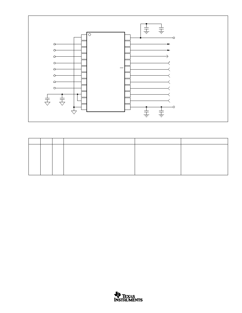
BASIC CIRCUIT CONFIGURATION
M0
M1
A0
TWO-CHANNEL/FOUR-CHANNEL OPERATION
DATA ON SERIAL OUTPUTS
CHANNELS CONVERTED
0
0
0
Two-Channel
A and B
A0 and B0
0
0
1
Two-Channel
A and B
A1 and B1
0
1
0
Two-Channel
A Only
A0 and B0
0
1
1
Two-Channel
A Only
A1 and B1
1
0
X
Four-Channel
A and B
Sequential
1
1
X
Four-Channel
A Only
Sequential
NOTE: X = Don't Care.
TRUTH TABLE
BGND
CH B1+
CH B1
CH B0+
CH B0
CH A1+
CH A1
CH A0+
CH A0
REF
IN
REF
OUT
AGND
1
2
3
4
5
6
7
8
9
10
11
12
24
23
22
21
20
19
18
17
16
15
14
13
BV
DD
SERIAL DATA A
SERIAL DATA B
BUSY
CLOCK
CS
RD
CONVST
A0
M0
M1
AV
DD
BUSY Output
Clock Input
Chip Select
Read Input
Conversion Start
A0 Address Select
M0 Address Select
M1 Address Select
ADS8361
10
µ
F
+
0.1
µ
F
+5V Analog Supply
+2.7V to +5.5V Digital Supply
10
µ
F
0.1
µ
F
+
10
µ
F
+
0.1
µ
F