Äîêóìåíòàöèÿ è îïèñàíèÿ www.docs.chipfind.ru
Burr Brown Products
from Texas Instruments
ADS8365
®
FEATURES
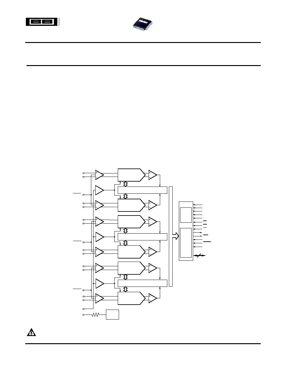
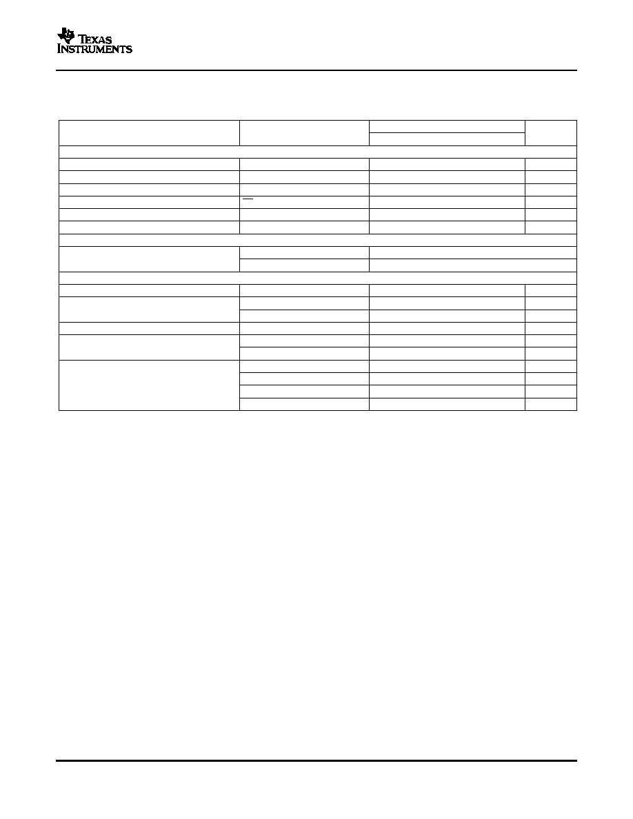
DESCRIPTION
APPLICATIONS
Interface
Conversion
and
Control
and
FIFO
Register
6x
EOC
FD
CS
WR
RD
Data
Input/Output
16
RESET
BYTE
CLK
CH
A0-
CH A0+
CH A1-
CH A1+
SAR
CDAC
S/H
Amp
Comp
CDAC
Comp
CH B0-
CH B0+
HOLDA
CH B1-
CH B1+
SAR
CDAC
Comp
CDAC
Comp
CH C0-
CH C0+
CH C1-
CH C1+
REF
IN
REF
OUT
SAR
CDAC
Comp
CDAC
Comp
HOLDB
HOLDC
ADD
A2
A1
A0
Internal
2.5V
Reference
S/H
Amp
S/H
Amp
S/H
Amp
S/H
Amp
S/H
Amp
NAP
ADS8365
SBAS362A AUGUST 2006 REVISED SEPTEMBER 2006
16-Bit, 250kSPS, 6-Channel, Simultaneous Sampling
SAR ANALOG-TO-DIGITAL CONVERTERS
·
Six Input Channels
The
ADS8365
includes
six,
16-bit,
250kSPS
analog-to-digital converters (ADCs) with six fully
·
Fully Differential Inputs
differential input channels grouped into three pairs
·
Six Independent 16-Bit ADCs
for
high-speed
simultaneous
signal
acquisition.
·
4
µ
s Total Throughput per Channel
Inputs to the sample-and-hold amplifiers are fully
·
Low Power:
differential and are maintained differential to the input
of the ADC. This architecture provides excellent
200mW in Normal Mode
common-mode rejection of 80dB at 50kHz, which is
5mW in Nap Mode
important in high-noise environments.
50
µ
W in Power-Down Mode
The ADS8365 offers a flexible, high-speed parallel
·
TQFP-64 Package Package
interface with a direct address mode, a cycle, and a
FIFO mode. The output data for each channel is
available as a 16-bit word.
·
Motor Control
·
Multi-Axis Positioning Systems
·
3-Phase Power Control
Please be aware that an important notice concerning availability, standard warranty, and use in critical applications of Texas
Instruments semiconductor products and disclaimers thereto appears at the end of this data sheet.
All trademarks are the property of their respective owners.
PRODUCTION DATA information is current as of publication date.
Copyright © 2006, Texas Instruments Incorporated
Products conform to specifications per the terms of the Texas
Instruments standard warranty. Production processing does not
necessarily include testing of all parameters.
www.ti.com
ABSOLUTE MAXIMUM RATINGS
(1)
DISSIPATION RATINGS
ADS8365
SBAS362A AUGUST 2006 REVISED SEPTEMBER 2006
This integrated circuit can be damaged by ESD. Texas Instruments recommends that all integrated circuits be handled with
appropriate precautions. Failure to observe proper handling and installation procedures can cause damage.
ESD damage can range from subtle performance degradation to complete device failure. Precision integrated circuits may be
more susceptible to damage because very small parametric changes could cause the device not to meet its published
specifications.
ORDERING INFORMATION
(1)
MAXIMUM
NO
INTEGRAL
MISSING
LINEARITY
CODES
SPECIFIED
TRANSPORT
ERROR
ERROR
PACKAGE-
PACKAGE
TEMPERATURE
PACKAGE
ORDERING
MEDIA,
PRODUCT
(LSB)
(LSB)
LEAD
DESIGNATOR
RANGE
MARKING
NUMBER
QUANTITY
ADS8365IPAG
Tray, 96
ADS8365
±
4
14
TQFP-64
PAG
40
°
C to +85
°
C
ADS8365I
Tape and
ADS8365IPAGR
Reel, 1500
(1)
For the most current package and ordering information, see the Package Option Addendum located at the end of this data sheet, or see
the TI website at www.ti.com.
over operating free-air temperature range (unless otherwise noted)
ADS8365
UNIT
Supply voltage, AGND to AV
DD
0.3 to 6
V
Supply voltage, BGND to BV
DD
0.3 to 6
V
Analog input voltage range
AGND 0.3 to AV
DD
+ 0.3
V
Reference input voltage range
AGND 0.3 to AV
DD
+ 0.3
V
Digital input voltage range
BGND 0.3 to BV
DD
+ 0.3
V
Ground voltage differences, AGND to BGND
±
0.3
V
Voltage differences, BV
DD
to AGND
0.3 to 6
V
Input current to any pin except supply
20 to 20
mA
Power dissipation
See Dissipation Ratings Table
Operating virtual junction temperature range, T
J
40 to +150
°
C
Operating free-air temperature range, T
A
40 to +85
°
C
Storage temperature range, T
STG
65 to +150
°
C
(1)
Stresses beyond those listed under Absolute Maximum Ratings may cause permanent damage to the device. These are stress ratings
only, and functional operation of the device at these or any other conditions beyond those indicated under Recommended Operating
Conditions is not implied. Exposure to absolute-maximum rated conditions for extended periods may affect device reliability.
DERATING
FACTOR ABOVE
T
A
+25
°
C
T
A
= +70
°
C
T
A
= +85
°
C
BOARD
PACKAGE
R
JC
R
JA
T
A
= +25
°
C
POWER RATING
POWER RATING
POWER RATING
Low-K
(1)
PAG
8.6
°
C/W
68.5
°
C/W
14.598mW/
°
C
1824mW
1168mW
949mW
High-K
(2)
PAG
8.6
°
C/W
42.8
°
C/W
23.364mW/
°
C
2920mW
1869mW
1519mW
(1)
The JEDEC Low K (1s) board design used to derive this data was a 3-inch x 3-inch, two-layer board with 2-ounce copper traces on top
of the board.
(2)
The JEDEC High K (2s2p) board design used to derive this data was a 3-inch x 3-inch, multilayer board with 1-ounce internal power and
ground planes, and 2-ounce copper traces on the top and bottom of the board.
2
Submit Documentation Feedback
www.ti.com
RECOMMENDED OPERATING CONDITIONS
ELECTRICAL CHARACTERISTICS: 100kSPS
ADS8365
SBAS362A AUGUST 2006 REVISED SEPTEMBER 2006
MIN
NOM
MAX
UNIT
Supply voltage, AV
DD
to AGND
4.75
5
5.25
V
Low-voltage levels
2.7
3.6
V
Supply voltage, BV
DD
to BGND
5V logic levels
4.5
5
5.5
V
Reference input voltage
1.5
2.5
2.6
V
Operating common-mode signal, IN
2.2
2.5
2.8
V
Analog inputs, +IN (IN)
0
±
V
REF
V
Operating junction temperature range, T
J
40
+125
°
C
Over recommended operating free-air temperature range at 40
°
C to +85
°
C, AV
DD
= 5V, BV
DD
= 3V, V
REF
= internal +2.5V, f
CLK
= 2MHz,
and f
SAMPLE
= 100kSPS, unless otherwise noted.
ADS8365
PARAMETER
TEST CONDITIONS
MIN
TYP
(1)
MAX
UNIT
ANALOG INPUT
Full-scale range
FSR +IN (IN)
±
V
REF
V
Operating common-mode signal
2.2
2.8
V
Input resistance
IN = V
REF
750
Input capacitance
IN = V
REF
25
pF
Input leakage current
IN = V
REF
±
1
nA
Differential input resistance
IN = V
REF
1500
Differential input capacitance
IN = V
REF
15
pF
At dc
84
dB
Common-mode rejection ratio
CMRR
V
IN
=
±
1.25V
PP
at 50kHz
80
dB
Bandwidth
BW FS sinewave, 3dB
10
MHz
DC ACCURACY
Resolution
16
Bits
No missing codes
NMC
14
Bits
Integral linearity error
INL
±
1.5
±
4
LSB
Differential nonlinearity
DNL
±
1.5
LSB
Bipolar offset error
V
OS
±
1
±
2.3
mV
Bipolar offset error match
Only pair-wise matching
0.2
1
mV
Bipolar offset error drift
TCV
OS
0.8
ppm/
°
C
Gain error
G
ERR
Referenced to V
REF
±
0.05
±
0.25
%FSR
Gain error match
Only pair-wise matching
0.005
0.05
%FSR
Gain error drift
TCG
ERR
2
ppm/
°
C
Noise
60
µ
Vrms
Power-supply rejection ratio
PSRR 4.75V < AV
DD
< 5.25V
87
dB
SAMPLING DYNAMICS
Conversion time per ADC
t
CONV
50kHz
f
CLK
5MHz
3.2
320
µ
s
Acquisition time
t
AQ
f
CLK
= 5MHz
800
ns
Aperture delay
5
ns
Aperture delay matching
100
ps
Aperture jitter
50
ps
Clock frequency
0.05
5
MHz
(1)
All typical values are at +25
°
C.
3
Submit Documentation Feedback
www.ti.com
ADS8365
SBAS362A AUGUST 2006 REVISED SEPTEMBER 2006
ELECTRICAL CHARACTERISTICS: 100kSPS (continued)
Over recommended operating free-air temperature range at 40
°
C to +85
°
C, AV
DD
= 5V, BV
DD
= 3V, V
REF
= internal +2.5V, f
CLK
= 2MHz,
and f
SAMPLE
= 100kSPS, unless otherwise noted.
ADS8365
PARAMETER
TEST CONDITIONS
MIN
TYP
(1)
MAX
UNIT
AC ACCURACY
Total harmonic distortion
THD V
IN
=
±
2.5V
PP
at 50kHz
94
dB
Spurious-free dynamic range
SFDR V
IN
=
±
2.5V
PP
at 50kHz
95
dB
Signal-to-noise ratio
SNR V
IN
=
±
2.5V
PP
at 10kHz
88
dB
Signal-to-noise + distortion
SINAD V
IN
=
±
2.5V
PP
at 10kHz
87
dB
Channel-to-channel isolation
95
dB
Effective number of bits
ENOB
14.3
Bits
VOLTAGE REFERENCE OUTPUT
Reference voltage output
V
OUT
2.475
2.5
2.525
V
Initial accuracy
±
1
%
Output voltage temperature drift
dV
OUT
/dT
±
20
ppm/
°
C
f = 0.1Hz to 10Hz, C
L
= 10
µ
F
40
µ
V
PP
Output voltage noise
f = 10Hz to 10kHz, C
L
= 10
µ
F
8
µ
Vrms
Power-supply rejection ratio
PSRR
60
dB
Output impedance
R
OUT
2
k
Short-circuit current
I
SC
1.25
mA
Turn-on settling time
to 0.1% at C
L
= 0pF
100
µ
s
VOLTAGE REFERENCE INPUT
Reference voltage input
V
IN
1.5
2.5
2.6
V
Reference input resistance
100
M
Reference input capacitance
5
pF
Reference input current
1
µA
DIGITAL INPUTS
(2)
Logic family
CMOS
High-level input voltage
V
IH
0.7
×
BV
DD
BV
DD
+ 0.3
V
Low-level input voltage
V
IL
0.3
0.3
×
BV
DD
V
Input current
I
IN
V
I
= BV
DD
or GND
±
50
nA
Input capacitance
C
I
5
pF
DIGITAL OUTPUTS
(2)
Logic family
CMOS
High-level output voltage
V
OH
BV
DD
= 4.5V, I
OH
= 100
µ
A
4.44
V
Low-level output voltage
V
OL
BV
DD
= 4.5V, I
OL
= 100
µ
A
0.5
V
High-impedance state output current
I
OZ
CS = BV
DD
, V
I
= BV
DD
or GND
±
50
nA
Output capacitance
C
O
5
pF
Load capacitance
C
L
30
pF
DIGITAL INPUTS
(3)
Logic family
LVCMOS
High-level input voltage
V
IH
BV
DD
= 3.6V
2
BV
DD
+ 0.3
V
Low-level input voltage
V
IL
BV
DD
= 2.7V
0.3
0.8
V
Input current
I
IN
V
I
= BV
DD
or GND
±
50
nA
Input capacitance
C
I
5
pF
(2)
Applies for 5.0V nominal supply: BV
DD
(min) = 4.5V and BV
DD
(max) = 5.5V.
(3)
Applies for 3.0V nominal supply: BV
DD
(min) = 2.7V and BV
DD
(max) = 3.6V.
4
Submit Documentation Feedback
www.ti.com
ADS8365
SBAS362A AUGUST 2006 REVISED SEPTEMBER 2006
ELECTRICAL CHARACTERISTICS: 100kSPS (continued)
Over recommended operating free-air temperature range at 40
°
C to +85
°
C, AV
DD
= 5V, BV
DD
= 3V, V
REF
= internal +2.5V, f
CLK
= 2MHz,
and f
SAMPLE
= 100kSPS, unless otherwise noted.
ADS8365
PARAMETER
TEST CONDITIONS
MIN
TYP
(1)
MAX
UNIT
DIGITAL OUTPUTS
(4)
Logic family
LVCMOS
High-level output voltage
V
OH
BV
DD
= 2.7V, I
OH
= 100
µ
A
BVDD 0.2
V
Low-level output voltage
V
OL
BV
DD
= 2.7V, I
OL
= 100
µ
A
0.2
V
High-impedance state output current
I
OZ
CS = BV
DD
, V
I
= BV
DD
or GND
±
50
nA
Output capacitance
C
O
5
pF
Load capacitance
C
L
30
pF
DATA FORMAT
Bit DB4 = 1
Binary two's complement
Data format
Bit DB4 = 0
Straight binary coding
POWER SUPPLY
Analog supply voltage
AV
DD
4.75
5.25
V
Low-voltage levels
2.7
3.6
V
Buffer I/O supply voltage
BV
DD
5V logic levels
4.5
5.5
V
Analog operating supply current
AI
DD
38
45
mA
BV
DD
= 3V
60
90
µ
A
Buffer I/O operating supply current
BI
DD
BV
DD
= 5V
100
150
µ
A
BV
DD
= 3V
190
225
mW
BV
DD
= 5V
190
225
mW
Power dissipation
Nap mode enabled
5
mW
Powerdown enabled
50
µ
W
(4)
Applies for 3.0V nominal supply: BV
DD
(min) = 2.7V and BV
DD
(max) = 3.6V.
5
Submit Documentation Feedback
Document Outline