ADS8402
SLAS154B ≠ DECEMBER 2002 ≠ REVISED MAY 2003
16-BIT, 1.25 MSPS, UNIPOLAR DIFFERENTIAL INPUT, MICRO POWER SAMPLING
ANALOG-TO-DIGITAL CONVERTER WITH PARALLEL INTERFACE AND REFERENCE
FEATURES
D
1.25-MHz Sample Rate
D
16-Bit NMC Ensured Over Temperature
D
Zero Latency
D
Unipolar Differential Input Range: V
ref
to ≠V
ref
D
Onboard Reference
D
Onboard Reference Buffer
D
High-Speed Parallel Interface
D
Power Dissipation: 155 mW at 1.25 MHz Typ
D
Wide Digital Supply
D
8-/16-Bit Bus Transfer
D
48-Pin TQFP Package
APPLICATIONS
D
DWDM
D
Instrumentation
D
High-Speed, High-Resolution, Zero Latency
Data Acquisition Systems
D
Transducer Interface
D
Medical Instruments
D
Communication
DESCRIPTION
The ADS8402 is a 16-bit, 1.25 MHz A/D converter with an
internal 4.096-V reference. The device includes a 16-bit
capacitor-based SAR A/D converter with inherent sample
and hold. The ADS8402 offers a full 16-bit interface and an
8-bit option where data is read using two 8-bit read cycles.
The ADS8402 has a unipolar differential input. It is
available in a 48-lead TQFP package and is characterized
over the industrial ≠40
∞
C to 85
∞
C temperature range.
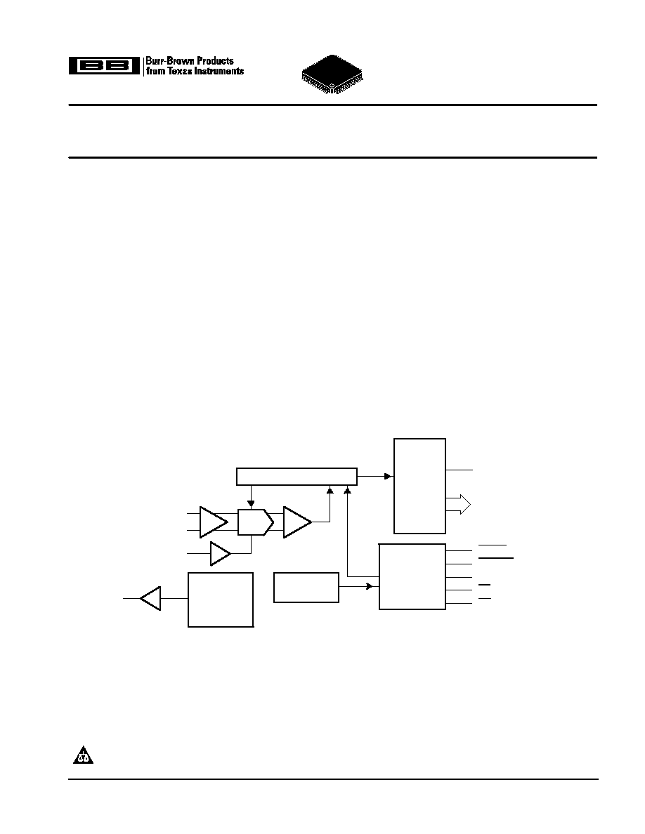
CDAC
_
+
Output
Latches
and
3-State
Drivers
BYTE
16-/8-Bit
Parallel DATA
Output Bus
SAR
Conversion
and
Control Logic
Comparator
Clock
+IN
≠IN
REFIN
CONVST
BUSY
CS
RD
RESET
4.096-V
Internal
Reference
REFOUT
PRODUCTION DATA information is current as of publication date. Products
conform to specifications per the terms of Texas Instruments standard warranty.
Production processing does not necessarily include testing of all parameters.
Please be aware that an important notice concerning availability, standard warranty, and use in critical applications of Texas Instruments
semiconductor products and disclaimers thereto appears at the end of this data sheet.
Copyright
2002≠2003, Texas Instruments Incorporated
ADS8402
SLAS154B ≠ DECEMBER 2002 ≠ REVISED MAY 2003
www.ti.com
2
These devices have limited built-in ESD protection. The leads should be shorted together or the device placed in conductive foam during
storage or handling to prevent electrostatic damage to the MOS gates.
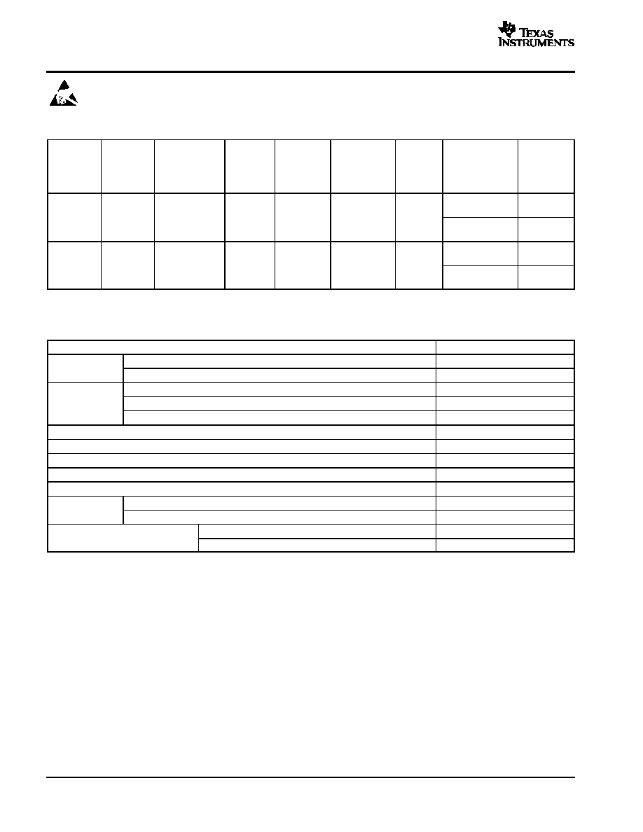
ORDERING INFORMATION
MODEL
MAXIMUM
INTEGRAL
LINEARITY
(LSB)
MAXIMUM
DIFFERENTIAL
LINEARITY
(LSB)
NO
MISSING
CODES
RESOLU-
TION (BIT)
PACKAGE
TYPE
PACKAGE
DESIGNATOR
TEMPER-
ATURE
RANGE
ORDERING
INFORMATION
TRANS-
PORT
MEDIA
QUANTITY
ADS8402I
±
6
2
3
15
48 Pin
PFB
≠40
∞
C to
ADS8402IPFBT
Tape and
reel 250
ADS8402I
±
6
≠2~+3
15
48 Pin
TQFP
PFB
≠40 C to
85
∞
C
ADS8402IPFBR
Tape and
reel 1000
ADS8402IB
±
3 5
1
2
16
48 Pin
PFB
≠40
∞
C to
ADS8402IBPFBT
Tape and
reel 250
ADS8402IB
±
3.5
≠1~+2
16
48 Pin
TQFP
PFB
≠40 C to
85
∞
C
ADS8402IBPFBR
Tape and
reel 1000
NOTE: For the most current specifications and package information, refer to our website at www.ti.com.
ABSOLUTE MAXIMUM RATINGS
over operating free-air temperature range unless otherwise noted(1)
UNIT
Voltage
+IN to AGND
+VA + 0.1 V
Voltage
≠IN to AGND
+VA + 0.1 V
+VA to AGND
≠0.3 V to 7 V
Voltage range
+VBD to BDGND
≠0.3 V to 7 V
Voltage range
+VA to +VBD
≠0.3 V to 2.5 V
Digital input voltage to BDGND
≠0.3 V to +VBD + 0.3 V
Digital output voltage to BDGND
≠0.3 V to +VBD + 0.3 V
Operating free-air temperature range, TA
≠40
∞
C to 85
∞
C
Storage temperature range, Tstg
≠65
∞
C to 150
∞
C
Junction temperature (TJ max)
150
∞
C
TQFP package
Power dissipation
(TJMax ≠ TA)/
JA
TQFP package
JA thermal impedance
86
∞
C/W
Lead temperature soldering
Vapor phase (60 sec)
215
∞
C
Lead temperature, soldering
Infrared (15 sec)
220
∞
C
(1) Stresses beyond those listed under "absolute maximum ratings" may cause permanent damage to the device. These are stress ratings only, and
functional operation of the device at these or any other conditions beyond those indicated under "recommended operating conditions" is not
implied. Exposure to absolute-maximum-rated conditions for extended periods may affect device reliability.
ADS8402
SLAS154B ≠ DECEMBER 2002 ≠ REVISED MAY 2003
www.ti.com
3
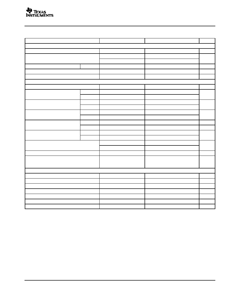
SPECIFICATIONS
TA = ≠40
∞
C to 85
∞
C, +VA = 5 V, +VBD = 3 V or 5 V, Vref = 4.096 V, fSAMPLE = 1.25 MHz (unless otherwise noted)
PARAMETER
TEST CONDITIONS
MIN
TYP
MAX
UNIT
Analog Input
Full-scale input voltage (see Note 1)
+IN ≠ ≠IN
≠Vref
Vref
V
Absolute input voltage
+IN
≠0.2
Vref + 0.2
V
Absolute input voltage
≠IN
≠0.2
Vref + 0.2
V
Common-mode input range
ADS8402I
(Vref
/2)
≠ 0.2
Vref/2
(Vref
/2)
+ 0.2
V
Input capacitance
25
pF
Input leakage current
0.5
nA
System Performance
Resolution
16
Bits
No missing codes
ADS8402I
15
Bits
No missing codes
ADS8402IB
16
Bits
Integral linearity (see Notes 2 and 3)
ADS8402I
≠6
±
2.5
6
LSB
Integral linearity (see Notes 2 and 3)
ADS8402IB
≠3.5
±
2
3.5
LSB
Differentiallinearity
ADS8402I
≠2
±
1
3
LSB
Differential linearity
ADS8402IB
≠1
±
0.75
2
LSB
Offset error (see Note 4)
ADS8402I
≠3
±
1
3
mV
Offset error (see Note 4)
ADS8402IB
≠1.5
±
0.5
1.5
mV
Gain error (see Notes 4 and 5)
ADS8402I
≠0.15
0.15
%FS
Gain error (see Notes 4 and 5)
ADS8402IB
≠0.098
0.098
%FS
Common mode rejection ratio
At dc (
±
0.2 V around Vref/2)
80
dB
Common-mode rejection ratio
+IN ≠ ≠IN = 1 Vpp at 1 MHz
80
dB
Noise
60
µ
V RMS
DC Power supply rejection ratio
At 7FFFh output code,
+VA = 4.75 V to 5.25 V,
Vref = 4.096 V, See Note 4
1
LSB
Sampling Dynamics
Conversion time
610
ns
Acquisition time
150
ns
Throughput rate
1.25
MHz
Aperture delay
2
ns
Aperture jitter
25
ps
Step response
100
ns
Overvoltage recovery
100
ns
(1) Ideal input span, does not include gain or offset error.
(2) LSB means least significant bit
(3) This is endpoint INL, not best fit
(4) Measured relative to an ideal full-scale input (+IN ≠ ≠IN) of 8.192 V
(5) This specification does not include the internal reference voltage error and drift.
ADS8402
SLAS154B ≠ DECEMBER 2002 ≠ REVISED MAY 2003
www.ti.com
4
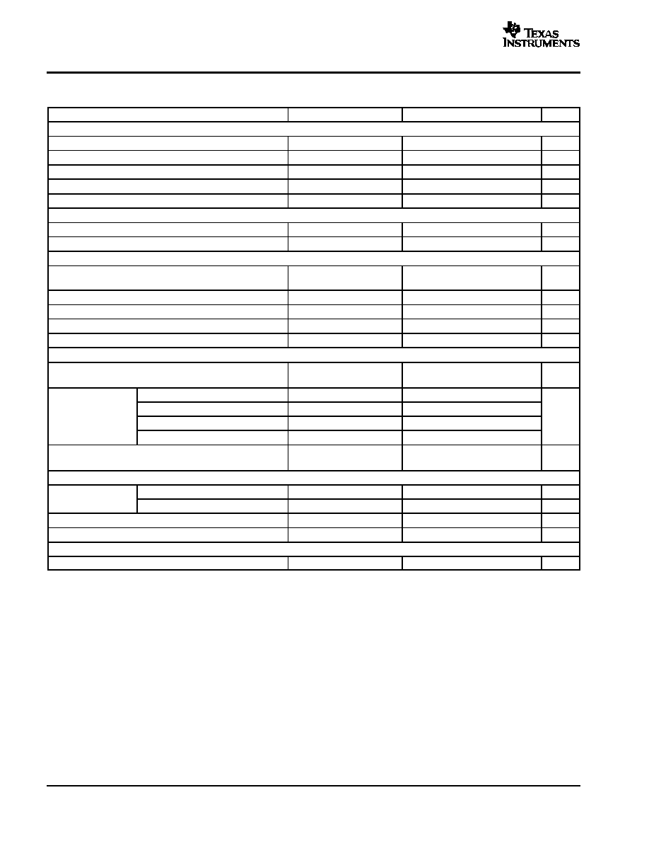
SPECIFICATIONS (CONTINUED)
TA = ≠40
∞
C to 85
∞
C, +VA = +5 V, +VBD = 3 V or 5 V, Vref = 4.096 V, fSAMPLE = 1.25 MHz (unless otherwise noted)
PARAMETER
TEST CONDITIONS
MIN
TYP
MAX
UNIT
Dynamic Characteristics
Total harmonic distortion (THD) (see Note 1)
VIN = 8 Vpp at 100 kHz
≠95
dB
Signal-to-noise ratio (SNR)
VIN = 8 Vpp at 100 kHz
90
dB
Signal-to-noise + distortion (SINAD)
VIN = 8 Vpp at 100 kHz
88
dB
Spurious free dynamic range (SFDR)
VIN = 8 Vpp at 100 kHz
95
dB
≠3dB Small signal bandwidth
5
MHz
External Voltage Reference Input
Reference voltage at REFIN, Vref
2.5
4.096
4.2
V
Reference resistance (see Note 2)
500
k
Internal Reference Output
Internal reference start-up time
From 95% (+VA), with 1
µ
F
storage capacity
120
ms
Vref range
IOUT = 0
4.065
4.096
4.13
V
Source Current
Static load
10
µ
A
Line Regulation
+VA = 4.75 ~ 5.25 V
0.6
mV
Drift
IOUT = 0
36
PPM/C
Digital Input/Output
Logic family
CMO
S
VIH
IIH = 5
µ
A
+VBD≠1
+VBD + 0.3
L
i l
l
VIL
IIL = 5
µ
A
≠0.3
0.8
V
Logic level
VOH
IOH = 2 TTL loads
+VBD ≠ 0.6
+VBD
V
VOL
IOL = 2 TTL loads
0
0.4
Data format
2's
Complement
Power Supply Requirements
P
l
lt
+VBD (see Notes 3 and 4)
2.95
3.3
5.25
V
Power supply voltage
+VA (see Note 4)
4.75
5
5.25
V
+VA Supply current (see Note 5)
fs = 1.25 MHz
31
34
mA
Power dissipation (see Note 5)
fs = 1.25 MHz
155
mW
Temperature Range
Operating free-air
≠40
85
∞
C
(1) Calculated on the first nine harmonics of the input frequency
(2) Can vary
±
20%
(3) The difference between +VA and +VBD should not be less than 2.3 V, i.e., if +VA is 5.25 V, +VBD should be minimum of 2.95 V.
(4) +VBD
+VA ≠ 2.3 V
(5) This includes only VA+ current. +VBD current is typically 1 mA with 5 pF load capacitance on output pins.
ADS8402
SLAS154B ≠ DECEMBER 2002 ≠ REVISED MAY 2003
www.ti.com
5
TIMING CHARACTERISTICS
All specifications typical at ≠40
∞
C to 85
∞
C, +VA = +VBD = 5 V (see Notes 1, 2, and 3)
PARAMETER
MIN
TYP
MAX
UNIT
tCONV
Conversion time
600
610
ns
tACQ
Acquisition time
150
ns
tpd1
CONVST low to conversion started (BUSY high)
35
ns
tpd2
Propagation delay time, End of conversion to BUSY low
20
ns
tw1
Pulse duration, CONVST low
20
ns
tsu1
Setup time, CS low to CONVST low
0
ns
tw2
Pulse duration, CONVST high
20
ns
CONVST falling edge jitter
10
ps
tw3
Pulse duration, BUSY signal low
Min(tACQ)
ns
tw4
Pulse duration, BUSY signal high
630
ns
th1
Hold time, First data bus data transition (RD low, or CS low for read cycle, or BYTE input
changes) after CONVST low
40
ns
td1
Delay time, CS low to RD low
0
ns
tsu2
Setup time, RD high to CS high
0
ns
tw5
Pulse duration, RD low time
50
ns
ten
Enable time, RD low (or CS low for read cycle) to data valid
20
ns
td2
Delay time, data hold from RD high
0
ns
td3
Delay time, BYTE rising edge
or falling edge to data valid
2
20
ns
tw6
RD high
20
ns
th2
Hold time, last RD (or CS for read cycle ) rising edge to CONVST falling edge
50
ns
tpd4
Propagation delay time, BUSY falling edge to next RD (or CS for read cycle) falling edge
Max(td5)
ns
tsu3
Setup time, BYTE rising edge to RD falling edge
0
ns
th3
Hold time, BYTE falling edge to RD falling edge
0
ns
tdis
Disable time, RD High (CS high for read cycle) to 3-stated data bus
20
ns
td5
Delay time, BUSY low to MSB data valid
0
ns
(1) All input signals are specified with tr = tf = 5 ns (10% to 90% of +VBD) and timed from a voltage level of (VIL + VIH)/2.
(2) See timing diagrams.
(3) All timings are measured with 20 pF equivalent loads on all data bits and BUSY pins.
ADS8402
SLAS154B ≠ DECEMBER 2002 ≠ REVISED MAY 2003
www.ti.com
6
TIMING CHARACTERISTICS
All specifications typical at ≠40
∞
C to 85
∞
C, +VA = 5 V, +VBD = 3 V (see Notes 1, 2, and 3)
PARAMETER
MIN
TYP
MAX
UNIT
tCONV
Conversion time
600
610
ns
tACQ
Acquisition time
150
ns
tpd1
CONVST low to conversion started (BUSY high)
40
ns
tpd2
Propagation delay time, end of conversion to BUSY low
20
ns
tw1
Pulse duration, CONVST low
20
ns
tsu1
Setup time, CS low to CONVST low
0
ns
tw2
Pulse duration, CONVST high
20
ns
CONVST falling edge jitter
10
ps
tw3
Pulse duration, BUSY signal low
Min(tACQ)
ns
tw4
Pulse duration, BUSY signal high
630
ns
th1
Hold time, first data bus transition (RD low, or CS low for read cycle, or BYTE or BUS
16/16 input changes) after CONVST low
40
ns
td1
Delay time, CS low to RD low
0
ns
tsu2
Setup time, RD high to CS high
0
ns
tw5
Pulse duration, RD low
50
ns
ten
Enable time, RD low (or CS low for read cycle) to data valid
30
ns
td2
Delay time, data hold from RD high
0
ns
td3
Delay time, BUS16/16
or
BYTE rising edge
or falling edge to data valid
2
30
ns
tw6
Pulse duration, RD high time
20
ns
th2
Hold time, last RD (or CS for read cycle ) rising edge to CONVST falling edge
50
ns
tpd4
Propagation delay time, BUSY falling edge to next RD (or CS for read cycle) falling edge
Max(td5)
ns
tsu3
Setup time, BYTE rising edge to RD falling edge
0
ns
th3
Hold time, BYTE falling edge to RD falling edge
0
ns
tdis
Disable time, RD High (CS high for read cycle) to 3-stated data bus
30
ns
td5
Delay time, BUSY low to MSB data valid delay time
0
ns
(1) All input signals are specified with tr = tf = 5 ns (10% to 90% of +VBD) and timed from a voltage level of (VIL + VIH)/2.
(2) See timing diagrams.
(3) All timings are measured with 10 pF equivalent loads on all data bits and BUSY pins.
ADS8402
SLAS154B ≠ DECEMBER 2002 ≠ REVISED MAY 2003
www.ti.com
7
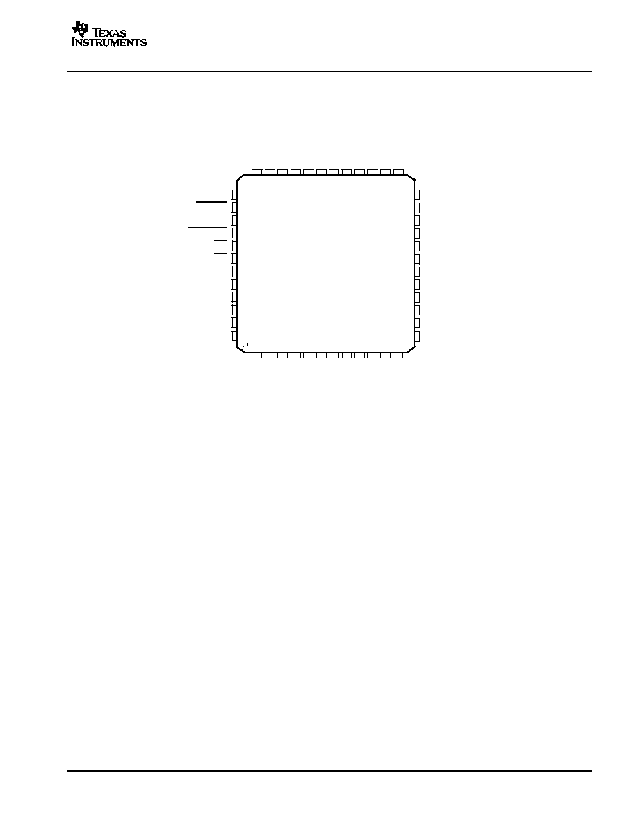
PIN ASSIGNMENTS
11
NC ≠ No connection
+VBD
DB8
DB9
DB10
DB11
DB12
DB13
DB14
DB15
AGND
AGND
+VA
1 2
37
38
39
40
41
42
43
44
45
46
47
48
+VBD
RESET
BYTE
CONVST
RD
CS
+VA
AGND
AGND
+VA
REFM
REFM
3
4 5
6
PFB PACKAGE
(TOP VIEW)
DB4
DB5
DB6
DB7
35 34 33 32 31
36
30
BUSY
BDGND
+VBD
DB0
DB1
DB2
DB3
AGND
+V
A
+V
A
REFIN
REFOUT
NC
+V
A
AGND
+IN
≠
IN
28 27 26
29
7 8
9 10
AGND
24
23
22
21
20
19
18
17
16
15
14
13
AGND
12
BDGND
25
ADS8402
SLAS154B ≠ DECEMBER 2002 ≠ REVISED MAY 2003
www.ti.com
8
TERMINAL FUNCTIONS
NAME
NO.
I/O
DESCRIPTION
AGND
5, 8, 11, 12,
14, 15, 44, 45
≠
Analog ground
BDGND
25, 35
≠
Digital ground for bus interface digital supply
BUSY
36
O
Status output. High when a conversion is in progress.
BYTE
39
I
Byte select input. Used for 8-bit bus reading.
0: No fold back
1: Low byte D[7:0] of the 16 most significant bits is folded back to high byte of the 16 most significant
pins DB[15:8].
CONVST
40
I
Convert start
CS
42
I
Chip select
D t B
8-Bit Bus
16-Bit Bus
Data Bus
BYTE = 0
BYTE = 1
BYTE = 0
DB15
16
O
D15 (MSB)
D7
D15 (MSB)
DB14
17
O
D14
D6
D14
DB13
18
O
D13
D5
D13
DB12
19
O
D12
D4
D12
DB11
20
O
D11
D3
D11
DB10
21
O
D10
D2
D10
DB9
22
O
D9
D1
D9
DB8
23
O
D8
D0 (LSB)
D8
DB7
26
O
D7
All ones
D7
DB6
27
O
D6
All ones
D6
DB5
28
O
D5
All ones
D5
DB4
29
O
D4
All ones
D4
DB3
30
O
D3
All ones
D3
DB2
31
O
D2
All ones
D2
DB1
32
O
D1
All ones
D1
DB0
33
O
D0 (LSB)
All ones
D0 (LSB)
≠IN
7
I
Inverting input channel
+IN
6
I
Non inverting input channel
NC
3
≠
No connection
REFIN
1
I
Reference input
REFM
47, 48
I
Reference ground
REFOUT
2
O
Reference output. Add 1
µ
F capacitor between the REFOUT pin and REFM pin when internal reference
is used.
RESET
38
I
Current conversion is aborted and output latches are cleared (set to zeros) when this pin is asserted low.
RESET works independantly of CS.
RD
41
I
Synchronization pulse for the parallel output.
+VA
4, 9, 10, 13,
43, 46
≠
Analog power supplies, 5-V dc
+VBD
24, 34, 37
≠
Digital power supply for bus
ADS8402
SLAS154B ≠ DECEMBER 2002 ≠ REVISED MAY 2003
www.ti.com
9
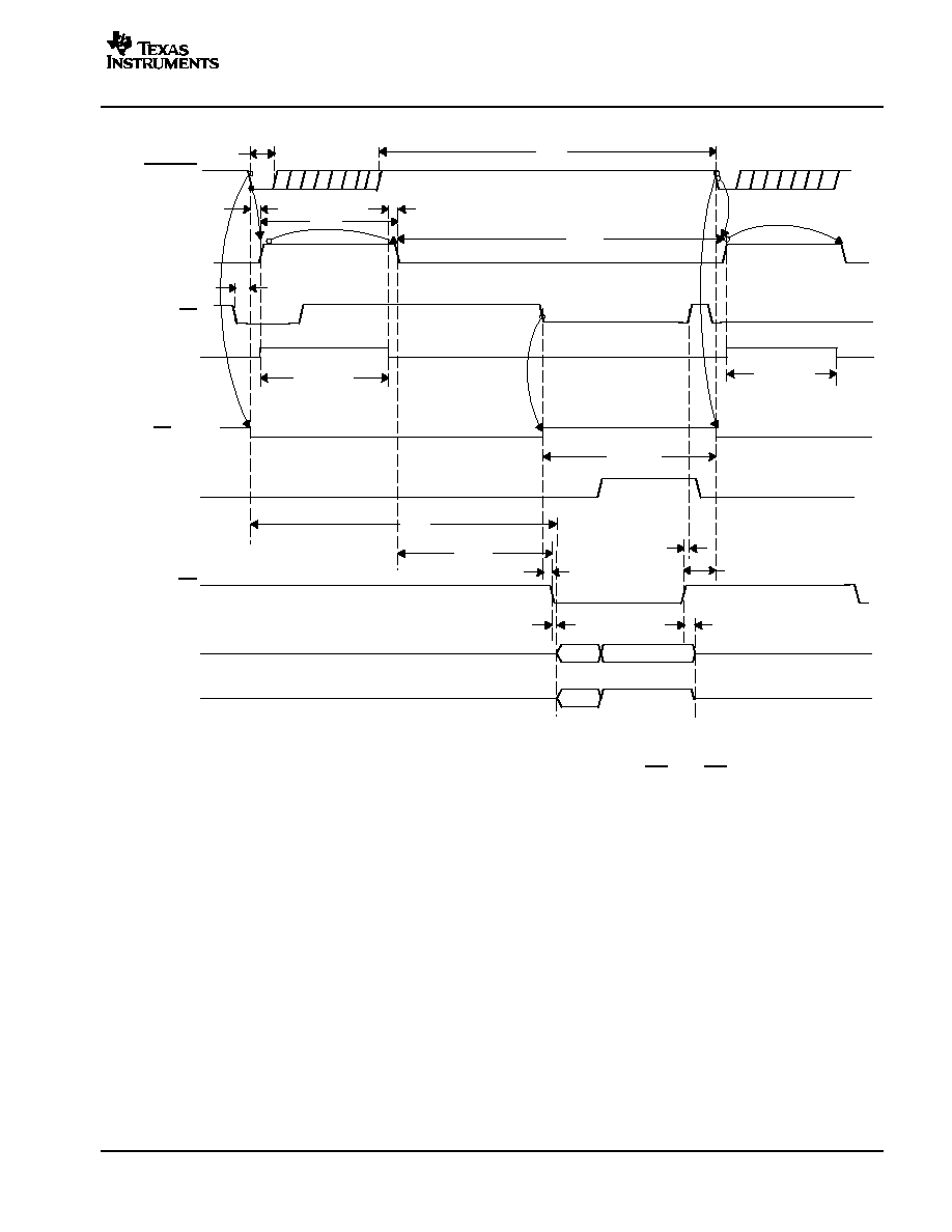
TIMING DIAGRAMS
tw1
CONVST
tpd1
tpd2
tw4
tsu1
BUSY
CS
CONVERT
t(CONV)
SAMPLING
(When CS Toggle)
BYTE
tw2
tw3
t(ACQ)
th1
tpd4
ten
RD
td1
tdis
th2
tsu2
t(CONV)
Signal internal to device
D [7:0]
Hi≠Z
Hi≠Z
DB[15:8]
Hi≠Z
Hi≠Z
D [15:8]
D [7:0]
DB[7:0]
Figure 1. Timing for Conversion and Acquisition Cycles With CS and RD Toggling
ADS8402
SLAS154B ≠ DECEMBER 2002 ≠ REVISED MAY 2003
www.ti.com
10
Signal internal to device
CONVST
BUSY
CS
CONVERT
SAMPLING
(When CS Toggle)
BYTE
RD = 0
tw1
tpd1
tpd2
tw4
tw2
tw3
tsu1
t(CONV)
t(ACQ)
t(CONV)
th1
tpd4
ten
th2
tdis
D [7:0]
Hi≠Z
Hi≠Z
DB[15:8]
Hi≠Z
Hi≠Z
D [15:8]
D [7:0]
DB[7:0]
Figure 2. Timing for Conversion and Acquisition Cycles With CS Toggling, RD Tied to BDGND
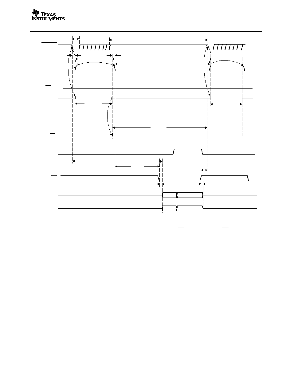
ADS8402
SLAS154B ≠ DECEMBER 2002 ≠ REVISED MAY 2003
www.ti.com
11
Signal internal to device
t(CONV)
CONVST
BUSY
CS = 0
CONVERT
SAMPLING
(When CS = 0)
BYTE
RD
tw1
tpd2
tpd1
tw4
tw2
tw3
t(CONV)
t(ACQ)
th1
tpd4
th2
ten
tdis
D [7:0]
Hi≠Z
Hi≠Z
DB[15:8]
Hi≠Z
Hi≠Z
D [15:8]
D [7:0]
DB[7:0]
Figure 3. Timing for Conversion and Acquisition Cycles With CS Tied to BDGND, RD Toggling
ADS8402
SLAS154B ≠ DECEMBER 2002 ≠ REVISED MAY 2003
www.ti.com
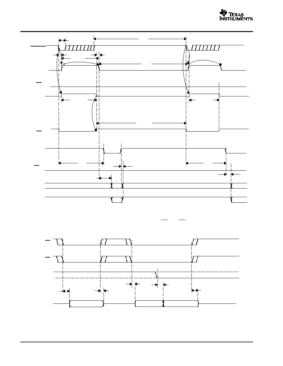
12
Signal internal to device
Previous D [7:0]
Next D [15:8]
tw1
tw2
tpd1
tpd2
tw4
t(CONV)
tw3
t(CONV)
t(ACQ)
th1
td5
th1
CONVST
BUSY
CS = 0
SAMPLING
(When CS = 0)
BYTE
RD = 0
DB[15:8]
D [7:0]
D [15:8]
D [7:0]
Next D [7:0]
DB[7:0]
CONVERT
tdis
td3
Figure 4. Timing for Conversion and Acquisition Cycles With CS and RD Tied to BDGND--Auto Read
Valid
Hi≠Z
ten
tdis
ten
td3
tdis
Valid
Valid
Hi≠Z
Hi≠Z
CS
RD
BYTE
DB[15:0]
Figure 5. Detailed Timing for Read Cycles
ADS8402
SLAS154B ≠ DECEMBER 2002 ≠ REVISED MAY 2003
www.ti.com
13
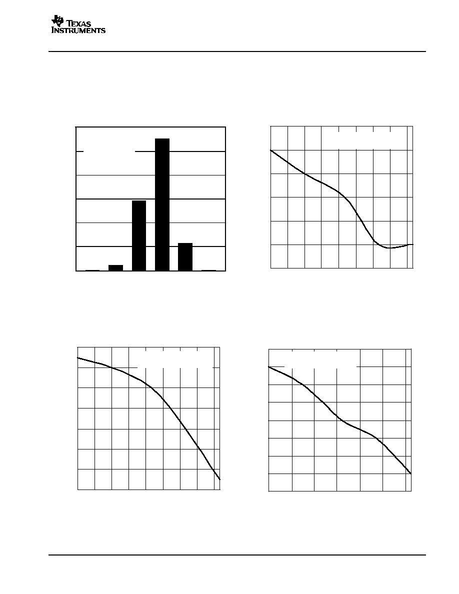
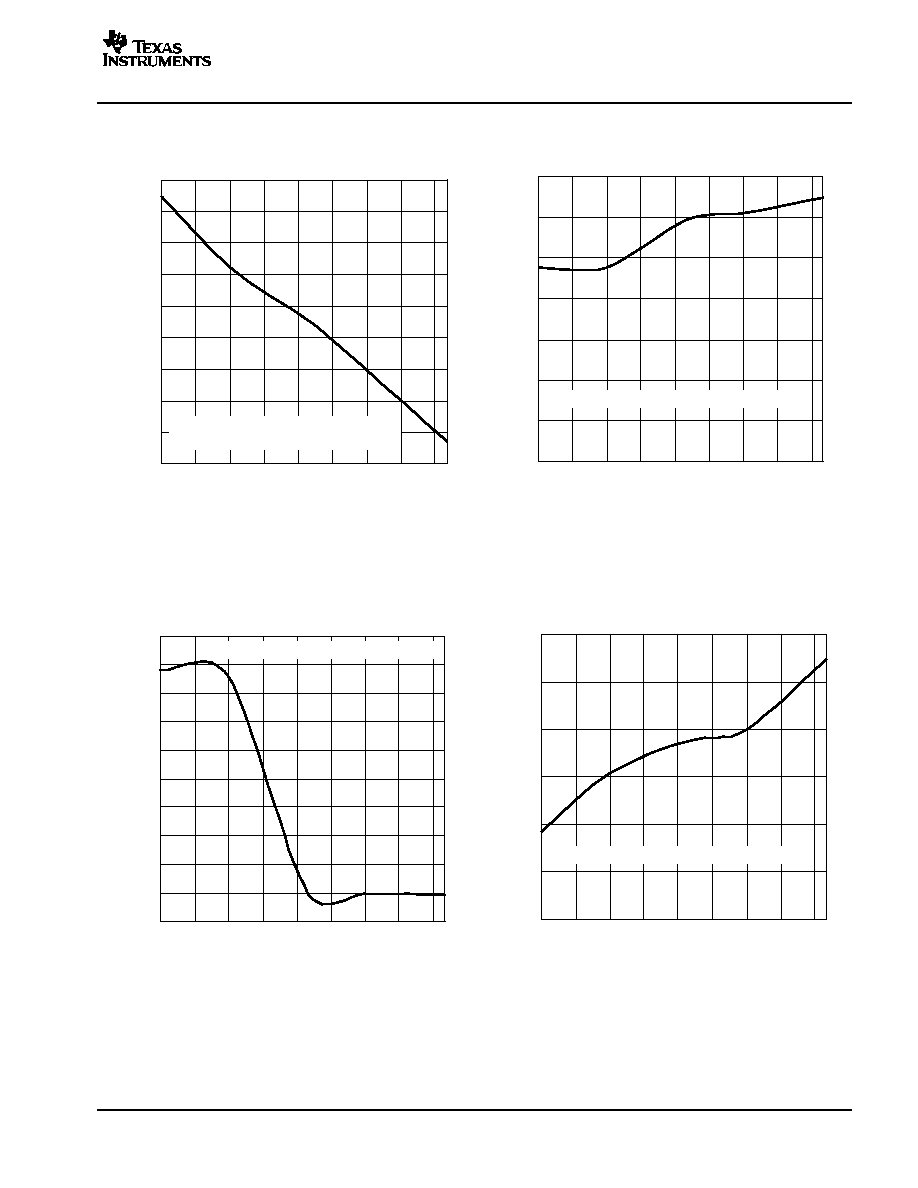
TYPICAL CHARACTERISTICS
Figure 6
0
20000
40000
60000
80000
100000
120000
HISTOGRAM (DC Code Spread)
NEAR POSITIVE FULL SCALE
196608 CONVERSIONS
+VA = 5 V,
Code = 61383
61380
61385
61383
Figure 7
SNR
≠
Signal-T
o- Noise Ratio
≠
dB
SIGNAL-TO-NOISE RATIO
vs
FREE-AIR TEMPERATURE
TA ≠ Free-Air Temperature ≠
∞
C
90.3
90.4
90.5
90.6
90.7
90.8
90.9
≠40
≠25
≠10
5
20
35
50
65
80
fi = 50 kHz
(+IN≠ ≠IN) = Full Scale
Figure 8
SINAD
≠
Signal-T
o-Noise Plus Distortion
≠
dB
SIGNAL-TO-NOISE PLUS DISTORTION
vs
FREE-AIR TEMPERATURE
TA ≠ Free-Air Temperature ≠
∞
C
89
89.2
89.4
89.6
89.8
90
90.2
90.4
≠40
≠25
≠10
5
20
35
50
65
80
fi = 50 kHz
(+IN≠ ≠IN) = Full Scale
Figure 9
≠40
0
40
80
≠20
20
60
SFDR
≠
Spurious Free-Dynamic Range
≠
dB
SPURIOUS FREE-DYNAMIC RANGE
vs
FREE-AIR TEMPERATURE
TA ≠ Free-Air Temperature ≠
∞
C
fi = 50 kHz
(+IN≠ ≠IN) = Full Scale
94
95
96
97
98
99
100
101
102
At ≠40
∞
C to 85
∞
C, +VA = 5 V, +VBD = 5 V, REFIN = 4.096 V (internal reference used) and fsample = 1.25 MHz (unless otherwise noted)
ADS8402
SLAS154B ≠ DECEMBER 2002 ≠ REVISED MAY 2003
www.ti.com
14
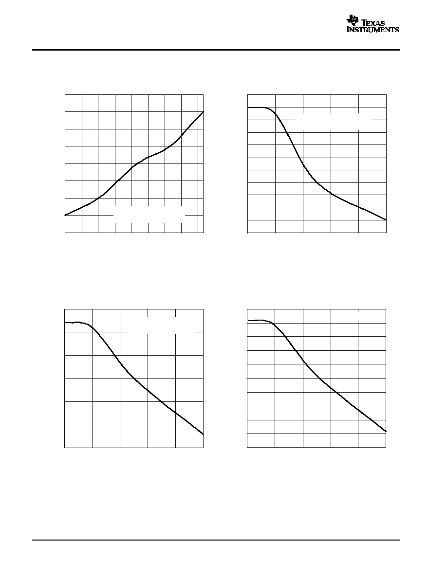
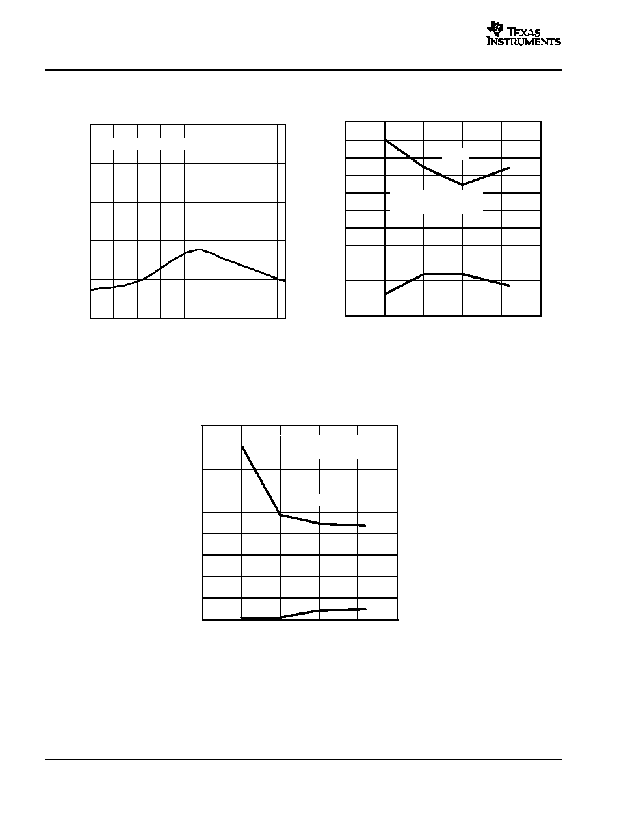
Figure 10
THD
≠
T
otal Harmonic Distortion
≠
dB
TOTAL HARMONIC DISTORTION
vs
FREE-AIR TEMPERATURE
TA ≠ Free-Air Temperature ≠
∞
C
≠102
≠101
≠100
≠99
≠98
≠97
≠96
≠95
≠94
≠40
≠25
≠10
5
20
35
50
65
80
fi = 50 kHz
(+IN≠ ≠IN) = Full Scale
Figure 11
SNR
≠
Signal-T
o- Noise Ratio
≠
dB
SIGNAL-TO-NOISE RATIO
vs
INPUT FREQUENCY
fi ≠ Input Frequency ≠ kHz
89.8
90
90.2
90.4
90.6
90.8
91
91.2
91.4
91.6
91.8
92
0
20
40
60
80
100
TA = 25
∞
C
(+IN≠ ≠IN) = Full Scale
Figure 12
SINAD
≠
Signal-T
o-Noise Plus Distortion
≠
dB
SIGNAL-TO-NOISE PLUS DISTORTION
vs
INPUT FREQUENCY
fi ≠ Input Frequency ≠ kHz
88.5
89
89.5
90
90.5
91
91.5
0
20
40
60
80
100
TA = 25
∞
C
(+IN≠ ≠IN) = Full Scale
14.4
14.45
14.5
14.55
14.6
14.65
14.7
14.75
14.8
14.85
14.9
0
20
40
60
80
100
ENOB
≠
Bit
ENOB
vs
INPUT FREQUENCY
fi ≠ Input Frequency ≠ kHz
Vref = 4.096 V
Figure 13
At ≠40
∞
C to 85
∞
C, +VA = 5 V, +VBD = 5 V, REFIN = 4.096 V (internal reference used) and fsample = 1.25 MHz (unless otherwise noted)
ADS8402
SLAS154B ≠ DECEMBER 2002 ≠ REVISED MAY 2003
www.ti.com
15
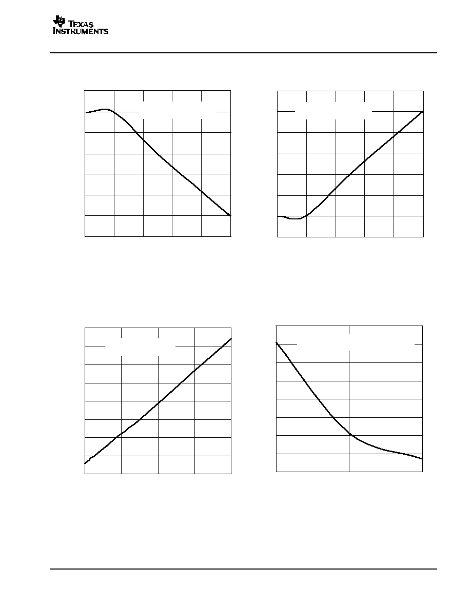
Figure 14
SFDR
≠
Spurious Free-Dynamic Range
≠
dB
SPURIOUS FREE-DYNAMIC RANGE
vs
INPUT FREQUENCY
fi ≠ Input Frequency ≠ kHz
0
20
40
60
80
100
TA = 25
∞
C
(+IN≠ ≠IN) = Full Scale
94
95
96
97
98
99
100
101
Figure 15
THD
≠
T
otal Harmonic Distortion
≠
dB
TOTAL HARMONIC DISTORTION
vs
INPUT FREQUENCY
fi ≠ Input Frequency ≠ kHz
≠101
≠100
≠99
≠98
≠97
≠96
≠95
≠94
0
20
40
60
80
100
TA = 25
∞
C
(+IN≠ ≠IN) = Full Scale
Figure 16
Sample Rate ≠ KSPS
SUPPLY CURRENT
vs
SAMPLE RATE
I CC
≠
Supply Current
≠
mA
28
28.5
29
29.5
30
30.5
31
31.5
32
250
500
750
1000
1250
TA = 25
∞
C
Current of +VA only
Figure 17
GAIN ERROR
vs
SUPPLY VOLTAGE
+VA ≠ Supply Voltage ≠ V
≠0.0024
≠0.0012
0
0.0012
0.0024
0.0036
0.0048
0.0061
0.0073
4.75
5
5.25
TA = 25
∞
C
External Reference = 4.096 V (REFIN)
≠
Gain Error
≠
%FS
E
G
At ≠40
∞
C to 85
∞
C, +VA = 5 V, +VBD = 5 V, REFIN = 4.096 V (internal reference used) and fsample = 1.25 MHz (unless otherwise noted)
ADS8402
SLAS154B ≠ DECEMBER 2002 ≠ REVISED MAY 2003
www.ti.com
16
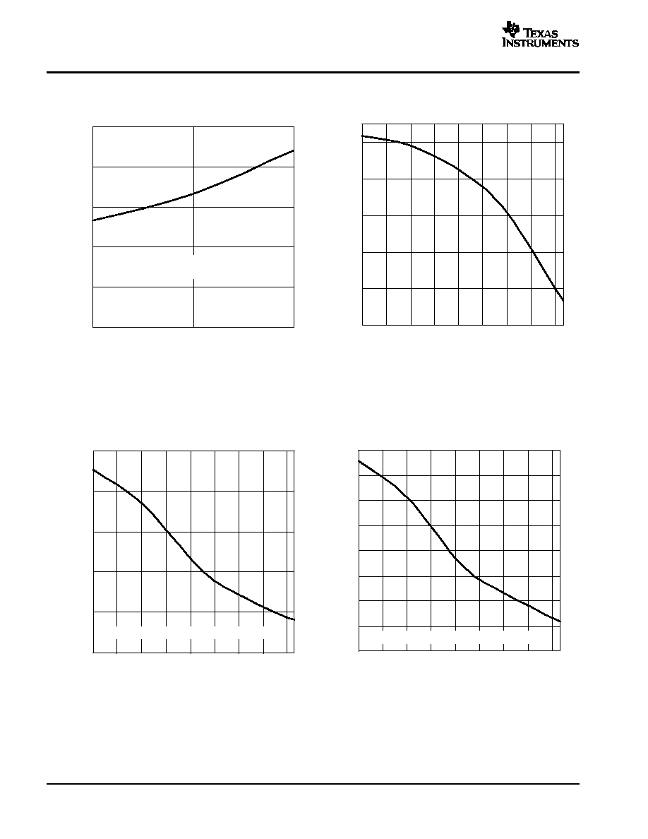
Figure 18
≠
Offset Error
≠
mV
OFFSET ERROR
vs
SUPPLY VOLTAGE
+VA ≠ Supply Voltage ≠ V
E
O
0
0.05
0.1
0.15
0.2
0.25
4.75
5
5.25
TA = 25
∞
C
External Reference = 4.096 V (REFIN)
Figure 19
≠
Internal Reference V
oltage
≠
V
INTERNAL REFERENCE VOLTAGE
vs
FREE-AIR TEMPERATURE
TA ≠ Free-Air Temperature ≠
∞
C
V
ref
4.088
4.090
4.092
4.094
4.096
4.098
≠40
≠25
≠10
5
20
35
50
65
80
Figure 20
GAIN ERROR
vs
FREE-AIR TEMPERATURE
TA ≠ Free-Air Temperature ≠
∞
C
≠0.012
≠0.006
0
0.006
0.012
0.018
≠40 ≠25
≠10
5
20
35
50
65
80
External Reference = 4.096 V (REFIN)
≠
Gain Error
≠
%FS
E
G
Figure 21
≠
Offset Error
≠
mV
OFFSET ERROR
vs
FREE-AIR TEMPERATURE
E
O
TA ≠ Free-Air Temperature ≠
∞
C
≠1
≠0.8
≠0.6
≠0.4
≠0.2
0
0.2
0.4
0.6
≠40
≠25
≠10
5
20
35
50
65
80
External Reference = 4.096 V (REFIN)
At ≠40
∞
C to 85
∞
C, +VA = 5 V, +VBD = 5 V, REFIN = 4.096 V (internal reference used) and fsample = 1.25 MHz (unless otherwise noted)
ADS8402
SLAS154B ≠ DECEMBER 2002 ≠ REVISED MAY 2003
www.ti.com
17
Figure 22
SUPPLY CURRENT
vs
FREE-AIR TEMPERATURE
I CC
≠
Supply Current
≠
mA
TA ≠ Free-Air Temperature ≠
∞
C
≠40
≠25
≠10
5
20
35
50
65
80
30.30
30.35
30.40
30.45
30.50
30.55
30.60
30.65
30.70
30.75
External Reference = 4.096 V (REFIN)
Current of +VA only
Figure 23
DNL
≠
Differential Nonlinearity (Max)
≠
LSB
DIFFERENTIAL NONLINEARITY (MAX)
vs
FREE-AIR TEMPERATURE
TA ≠ Free-Air Temperature ≠
∞
C
0
0.2
0.4
0.6
0.8
1
1.2
1.4
≠40
≠25
≠10
5
20
35
50
65
80
External Reference = 4.096 V (REFIN)
Figure 24
DNL
≠
Differential Nonlinearity (MIN)
≠
LSB
DIFFERENTIAL NONLINEARITY (MIN)
vs
FREE-AIR TEMPERATURE
TA ≠ Free-Air Temperature ≠
∞
C
≠0.78
≠0.77
≠0.76
≠0.75
≠0.74
≠0.73
≠0.72
≠0.71
≠0.70
≠0.69
≠0.68
≠40
≠25
≠10
5
20
35
50
65
80
External Reference = 4.096 V (REFIN)
Figure 25
0
0.5
1
1.5
2
2.5
3
≠40
≠25
≠10
5
20
35
50
65
80
INL
≠
Integral Nonlinearity (MAX)
≠
LSB
INTEGRAL NONLINEARITY (MAX)
vs
FREE-AIR TEMPERATURE
TA ≠ Free-Air Temperature ≠
∞
C
External Reference = 4.096 V (REFIN)
At ≠40
∞
C to 85
∞
C, +VA = 5 V, +VBD = 5 V, REFIN = 4.096 V (internal reference used) and fsample = 1.25 MHz (unless otherwise noted)
ADS8402
SLAS154B ≠ DECEMBER 2002 ≠ REVISED MAY 2003
www.ti.com
18
Figure 26
INL
≠
Integral Nonlinearity (MIN)
≠
LSB
INTEGRAL NONLINEARITY (MIN)
vs
FREE-AIR TEMPERATURE
TA ≠ Free-Air Temperature ≠
∞
C
≠2.5
≠2
≠1.5
≠1
≠0.5
0
≠40
≠25
≠10
5
20
35
50
65
80
External Reference = 4.096 V (REFIN)
Figure 27
≠2.5
≠2.0
≠1.5
≠1.0
≠0.5
0.0
0.5
1.0
1.5
2.0
2.5
3.0
2.0
2.5
3.0
3.5
4.0
4.5
INL
≠
Integral Nonlinearity
≠
LSB
INTEGRAL NONLINEARITY
vs
REFERENCE VOLTAGE
Vref ≠ Reference Voltage ≠ V
+VA = +VBD = 5 V,
TA = 25
∞
C
Min
Max
Figure 28
≠1.0
≠0.5
0.0
0.5
1.0
1.5
2.0
2.5
3.0
3.5
2.0
2.5
3.0
3.5
4.0
4.5
DNL
≠
Differential Nonlinearity
≠
LSB
DIFFERENTIAL NONLINEARITY
vs
REFERENCE VOLTAGE
Vref ≠ Reference Voltage ≠ V
+VA = +VBD = 5 V,
TA = 25
∞
C
Max
Min
At ≠40
∞
C to 85
∞
C, +VA = 5 V, +VBD = 5 V, REFIN = 4.096 V (internal reference used) and fsample = 1.25 MHz (unless otherwise noted)
ADS8402
SLAS154B ≠ DECEMBER 2002 ≠ REVISED MAY 2003
www.ti.com
19
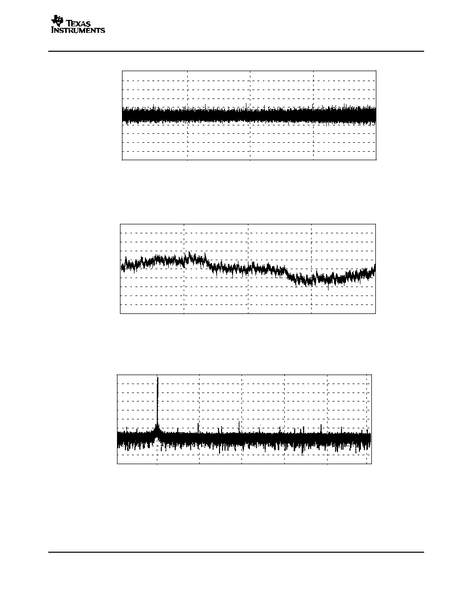
Figure 29
TA = 25
∞
C, External Reference = 4.096 V (REFIN)
0
16384
32768
DNL
≠
LSB
Code
DNL
49152
65536
≠0.5
≠1
1
0
0.5
1.5
2
2.5
≠1.5
≠2
≠2.5
Figure 30
TA = 25
∞
C, External Reference = 4.096 V (REFIN)
≠1
≠3
0
16384
32768
1
3
49152
65536
≠2
≠0
2
INL
≠
LSB
Code
INL
≠4
≠5
4
5
Figure 31
≠160
≠200
0
100
300
≠100
≠60
0
400
≠180
≠120
≠140
≠80
≠40
≠20
Magnitude
≠
dB of Full Scale
Frequency ≠ kHz
FFT SPECTRUM RESPONSE
600
500
200
32768 Points, fS = 1.25 MHz,
Internal Reference = 4.096 V (REFIN),
TA = 25
∞
C, fi = 100 kHz, (+IN≠ ≠IN) = Full Scale
At ≠40
∞
C to 85
∞
C, +VA = 5 V, +VBD = 5 V, REFIN = 4.096 V (internal reference used) and fsample = 1.25 MHz (unless otherwise noted)
ADS8402
SLAS154B ≠ DECEMBER 2002 ≠ REVISED MAY 2003
www.ti.com
20
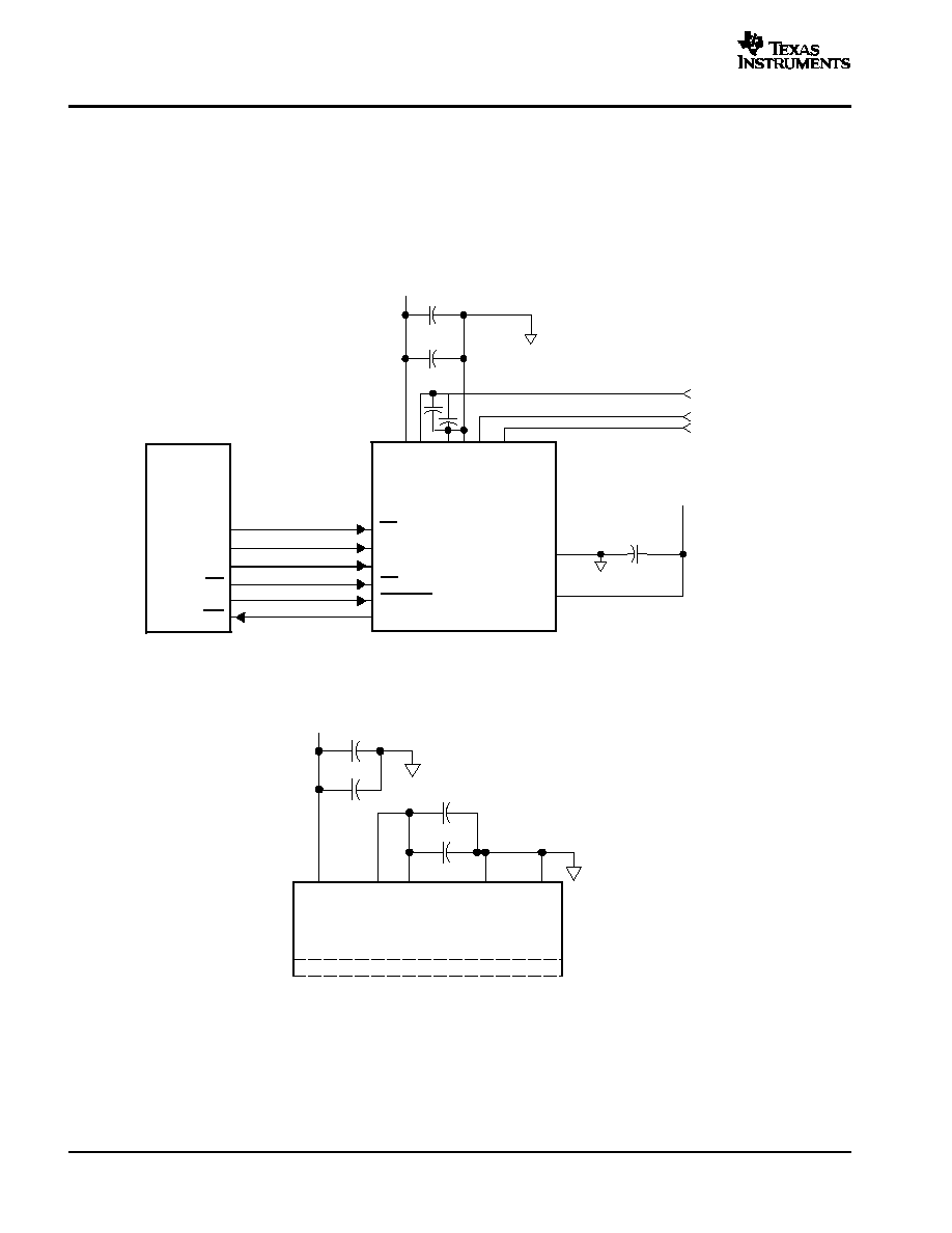
APPLICATION INFORMATION
MICROCONTROLLER INTERFACING
ADS8402 to 8-Bit Microcontroller Interface
Figure 32 shows a parallel interface between the ADS8402 and a typical microcontroller using the 8-bit data bus.
The BUSY signal is used as a falling-edge interrupt to the microcontroller.
CS
RD
CONVST
BUSY
BDGND
+VBD
DB[15:8]
Micro
Controller
RD
GPIO
INT
10
µ
F
0.1
µ
F
Analog 5 V
0.1
µ
F
Digital 3 V
Ext Ref Input
Analog Input
+V
A
REFM
AGND
+IN
≠
IN
ADS8402
0.1
µ
F
REFIN
1
µ
F
AGND
BDGND
P[7:0]
GPIO
BYTE
GPIO
Figure 32. ADS8402 Application Circuitry (using external reference)
+V
A
REFOUT
REFIN
REFM
AGND
0.1
µ
F
1
µ
F
0.1
µ
F
10
µ
F
Analog 5 V
ADS8402
AGND
AGND
Figure 33. Use Internal Reference

ADS8402
SLAS154B ≠ DECEMBER 2002 ≠ REVISED MAY 2003
www.ti.com
21
PRINCIPLES OF OPERATION
The ADS8402 is a high-speed successive approximation register (SAR) analog-to-digital converter (ADC). The
architecture is based on charge redistribution, which inherently includes a sample/hold function. See Figure 32 for
the application circuit for the ADS8402.
The conversion clock is generated internally. The conversion time of 610 ns is capable of sustaining a 1.25-MHz
throughput.
The analog input is provided to two input pins: +IN and ≠IN. When a conversion is initiated, the differential input on
these pins is sampled on the internal capacitor array. While a conversion is in progress, both inputs are disconnected
from any internal function.
REFERENCE
The ADS8402 can operate with an external reference with a range from 2.5 V to 4.2 V. A 4.096-V internal reference
is included. When internal reference is used, pin 2 (REFOUT) should be connected to pin 1 (REFIN) with an 0.1
µ
F
decoupling capacitor and 1
µ
F storage capacitor between pin 2 (REFOUT) and pins 47 and 48 (REFM) (see
Figure 33). The internal reference of the converter is double buffered. If an external reference is used, the second
buffer provides isolation between the external reference and the CDAC. This buffer is also used to recharge all of
the capacitors of the CDAC during conversion. Pin 2 (REFOUT) can be left unconnected (floating) if external
reference is used.
ANALOG INPUT
When the converter enters the hold mode, the voltage difference between the +IN and ≠IN inputs is captured on the
internal capacitor array. Both +IN and ≠IN input has a range of ≠0.2 V to V
ref
+ 0.2 V. The input span
(+IN ≠ (≠IN)) is limited to ≠V
ref
to V
ref
.
The input current on the analog inputs depends upon a number of factors: sample rate, input voltage, and source
impedance. Essentially, the current into the ADS8402 charges the internal capacitor array during the sample period.
After this capacitance has been fully charged, there is no further input current. The source of the analog input voltage
must be able to charge the input capacitance (25 pF) to an 16-bit settling level within the acquisition time (150 ns)
of the device. When the converter goes into the hold mode, the input impedance is greater than 1 G
.
Care must be taken regarding the absolute analog input voltage. To maintain the linearity of the converter, the +IN
and ≠IN inputs and the span (+IN ≠ (≠IN)) should be within the limits specified. Outside of these ranges, the
converter's linearity may not meet specifications. To minimize noise, low bandwidth input signals with low-pass filters
should be used.
Care should be taken to ensure that the output impedance of the sources driving +IN and ≠IN inputs are matched.
If this is not observed, the two inputs could have different setting time. This may result in offset error, gain error and
linearity error which varies with temperature and input voltage.
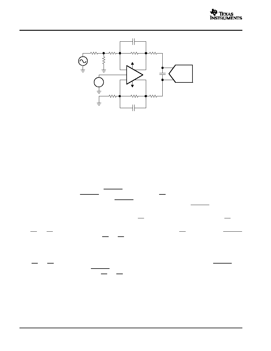
A typical input circuit using TI's THS4503 is shown in Figure 34. Input from a single-ended source may be converted
into differential signal for ADS8402 as shown in the figure. In case the source itself is differential then THS4503 may
be used in differential input and differential output mode.
ADS8402
SLAS154B ≠ DECEMBER 2002 ≠ REVISED MAY 2003
www.ti.com
22
_
+
_
+
IN≠
IN+
ADS8402
_
+
VCC+
VCC≠
1 k
1 k
THS4503
68 pF
68 pF
50
50
20 pF
RG
RS
RT
OCM
1 k
RG, RS, and RT should be chosen such that
RG + RS || RT = 1 k
VOCM = 2 V, +VCC = 7 V, and ≠VCC = ≠7 V
Figure 34. Using THS4503 With ADS8402
DIGITAL INTERFACE
Timing and Control
See the timing diagrams in the specifications section for detailed information on timing signals and their requirements.
The ADS8402 uses an internal oscillator generated clock which controls the conversion rate and in turn the
throughput of the converter. No external clock input is required.
Conversions are initiated by bringing the CONVST pin low for a minimum of 20 ns (after the 20 ns minimum
requirement has been met, the CONVST pin can be brought high), while CS is low. The ADS8402 switches from the
sample to the hold mode on the falling edge of the CONVST command. A clean and low jitter falling edge of this signal
is important to the performance of the converter. The BUSY output is brought high after CONVST goes low. BUSY
stays high throughout the conversion process and returns low when the conversion has ended.
Sampling starts with the falling edge of the BUSY signal when CS is tied low or starts with the falling edge of CS when
BUSY is low.
Both RD and CS can be high during and before a conversion with one exception (CS must be low when CONVST
goes low to initiate a conversion). Both the RD and CS pins are brought low in order to enable the parallel output bus
with the conversion.
Reading Data
The ADS8402 outputs full parallel data in two's complement format as shown in Table 1. The parallel output is active
when CS and RD are both low. There is a minimal quiet zone requirement around the falling edge of CONVST. This
is 100 ns prior to the falling edge of CONVST and 40 ns after the falling edge. No data read should be attempted
within this zone. Any other combination of CS and RD sets the parallel output to 3-state. BYTE is used for multiword
read operations. BYTE is used whenever lower bits of the conversion result are output on the higher byte of the bus.
Refer to Table 1 for ideal output codes.
ADS8402
SLAS154B ≠ DECEMBER 2002 ≠ REVISED MAY 2003
www.ti.com
23
Table 1. Ideal Input Voltages and Output Codes
DESCRIPTION
ANALOG VALUE
DIGITAL OUTPUT TWOS COMPLEMENT
FULL SCALE RANGE
2Vref
DIGITAL OUTPUT TWOS COMPLEMENT
Least significant bit (LSB)
2Vref/65536
BINARY CODE
HEX CODE
Full scale
Vref
0111 1111 1111 1111
7FFF
Midscale
0
0000 0000 0000 0000
0000
Zero
≠Vref
1000 0000 0000 0000
8000
The output data is a full 16-bit word (D15≠D0) on DB15≠DB0 pins (MSB≠LSB) if BYTE is low.
The result may also be read on an 8-bit bus for convenience. This is done by using only pins DB15≠DB8. In this case
two reads are necessary: the first as before, leaving BYTE low and reading the 8 most significant bits on pins
DB15≠DB8, then bringing BYTE high. When BYTE is high, the low bits (D7≠D0) appears on pins DB15≠D8.
These multiword read operations can be done with multiple active RD (toggling) or with RD tied low for simplicity.
BYTE
DATA READ OUT
BYTE
DB15≠DB8
DB7≠DB0
High
D7≠D0
All one's
Low
D15≠D8
D7≠D0
RESET
RESET is an asynchronous active low input signal (that works independantly of CS). Minimum RESET low time is
20 ns. Current conversion will be aborted no later than 50 ns after the converter is in the reset mode. In addition, all
output latches are cleared (set to zero's) after RESET. The converter goes back to normal operation mode no later
than 20 ns after RESET input is brought high.
The converter starts the first sampling period 20 ns after the rising edge of RESET. Any sampling period except for
the one immediately after a RESET is started with the falling edge of the previous BUSY signal or the falling edge
of CS, whichever is later.
POWER-ON INITIALIZATION
One RESET pulse followed by three conversion cycles must be given to the converter after powerup to ensure proper
operation. The next pulse can be issued once both +VA and +VBD reach 95% of the minimum required value.
LAYOUT
For optimum performance, care should be taken with the physical layout of the ADS8402 circuitry.
As the ADS8402 offers single-supply operation, it is often used in close proximity with digital logic, microcontrollers,
microprocessors, and digital signal processors. The more digital logic present in the design and the higher the
switching speed, the more difficult it is to achieve good performance from the converter.
The basic SAR architecture is sensitive to glitches or sudden changes on the power supply, reference, ground
connections and digital inputs that occur just prior to latching the output of the analog comparator. Thus, driving any
single conversion for an n-bit SAR converter, there are at least n windows in which large external transient voltages
can affect the conversion result. Such glitches might originate from switching power supplies, nearby digital logic,
or high power devices.
The degree of error in the digital output depends on the reference voltage, layout, and the exact timing of the external
event.
On average, the ADS8402 draws very little current from an external reference, as the reference voltage is internally
buffered. If the reference voltage is external and originates from an op amp, make sure that it can drive the bypass
capacitor or capacitors without oscillation. A 0.1-
µ
F bypass capacitor and 1-
µ
F storage capacitor are recommended
from pin 1 (REFIN) directly to pin 48 (REFM). REFM and AGND should be shorted on the same ground plane under
the device.
ADS8402
SLAS154B ≠ DECEMBER 2002 ≠ REVISED MAY 2003
www.ti.com
24
The AGND and BDGND pins should be connected to a clean ground point. In all cases, this should be the analog
ground. Avoid connections which are close to the grounding point of a microcontroller or digital signal processor. If
required, run a ground trace directly from the converter to the power supply entry point. The ideal layout consists of
an analog ground plane dedicated to the converter and associated analog circuitry.
As with the AGND connections, +VA
should be connected to a 5-V power supply plane or trace that is separate from
the connection for digital logic until they are connected at the power entry point. Power to the ADS8402 should be
clean and well bypassed. A 0.1-
µ
F ceramic bypass capacitor should be placed as close to the device as possible.
See Table 2 for the placement of the capacitor. In addition, a 1-
µ
F to 10-
µ
F capacitor is recommended. In some
situations, additional bypassing may be required, such as a 100-
µ
F electrolytic capacitor or even a Pi filter made up
of inductors and capacitors--all designed to essentially low-pass filter the 5-V supply, removing the high frequency
noise.
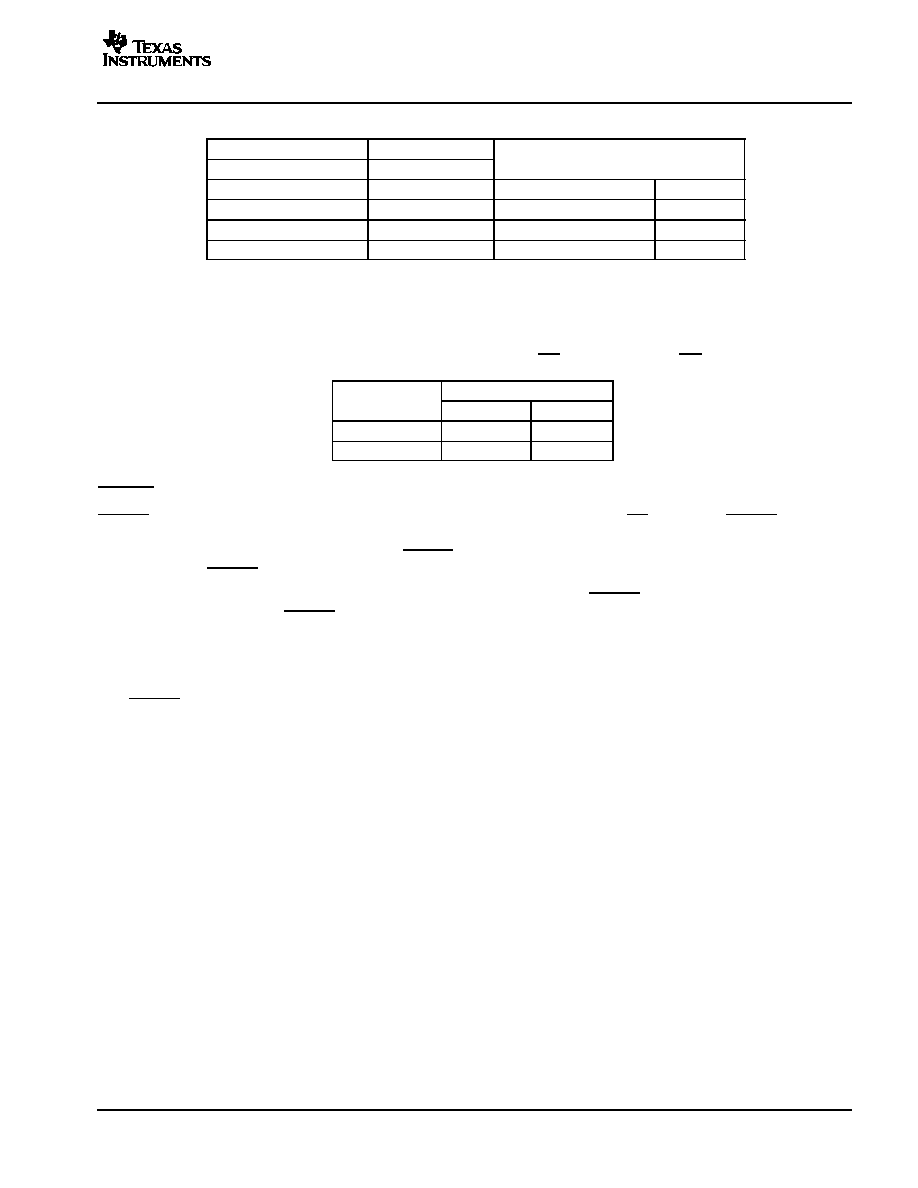
Table 2. Power Supply Decoupling Capacitor Placement
POWER SUPPLY PLANE
CONVERTER ANALOG SIDE
CONVERTER DIGITAL SIDE
SUPPLY PINS
CONVERTER ANALOG SIDE
CONVERTER DIGITAL SIDE
Pin pairs that require shortest path to decoupling capacitors
(4,5), (8,9), (10,11), (13,15),
(43,44), (45,46)
(24,25), (34, 35)
Pins that require no decoupling
12, 14
37

IMPORTANT NOTICE
Texas Instruments Incorporated and its subsidiaries (TI) reserve the right to make corrections, modifications,
enhancements, improvements, and other changes to its products and services at any time and to discontinue
any product or service without notice. Customers should obtain the latest relevant information before placing
orders and should verify that such information is current and complete. All products are sold subject to TI's terms
and conditions of sale supplied at the time of order acknowledgment.
TI warrants performance of its hardware products to the specifications applicable at the time of sale in
accordance with TI's standard warranty. Testing and other quality control techniques are used to the extent TI
deems necessary to support this warranty. Except where mandated by government requirements, testing of all
parameters of each product is not necessarily performed.
TI assumes no liability for applications assistance or customer product design. Customers are responsible for
their products and applications using TI components. To minimize the risks associated with customer products
and applications, customers should provide adequate design and operating safeguards.
TI does not warrant or represent that any license, either express or implied, is granted under any TI patent right,
copyright, mask work right, or other TI intellectual property right relating to any combination, machine, or process
in which TI products or services are used. Information published by TI regarding third≠party products or services
does not constitute a license from TI to use such products or services or a warranty or endorsement thereof.
Use of such information may require a license from a third party under the patents or other intellectual property
of the third party, or a license from TI under the patents or other intellectual property of TI.
Reproduction of information in TI data books or data sheets is permissible only if reproduction is without
alteration and is accompanied by all associated warranties, conditions, limitations, and notices. Reproduction
of this information with alteration is an unfair and deceptive business practice. TI is not responsible or liable for
such altered documentation.
Resale of TI products or services with statements different from or beyond the parameters stated by TI for that
product or service voids all express and any implied warranties for the associated TI product or service and
is an unfair and deceptive business practice. TI is not responsible or liable for any such statements.
Mailing Address:
Texas Instruments
Post Office Box 655303
Dallas, Texas 75265
Copyright
2003, Texas Instruments Incorporated