Burr Brown Products
from Texas Instruments
FEATURES
APPLICATIONS
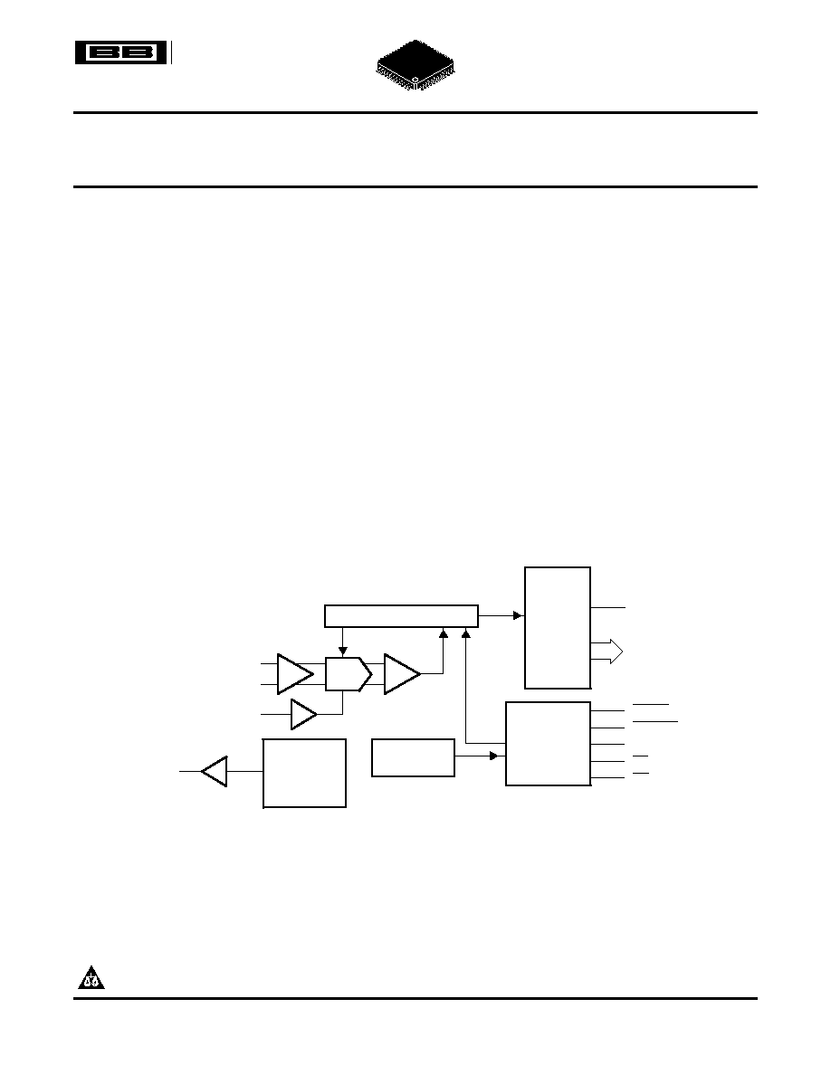
DESCRIPTION
CDAC
_
+
Output
Latches
and
3-State
Drivers
BYTE
16-/8-Bit
Parallel DATA
Output Bus
SAR
Conversion
and
Control Logic
Comparator
Clock
+IN
-IN
REFIN
CONVST
BUSY
CS
RD
RESET
4.096-V
Internal
Reference
REFOUT
ADS8412
SLAS384A ≠ JUNE 2003 ≠ REVISED DECEMBER 2004
16-BIT, 2 MSPS, UNIPOLAR DIFFERENTIAL INPUT, MICROPOWER SAMPLING
ANALOG-TO-DIGITAL CONVERTER WITH PARALLEL INTERFACE AND REFERENCE
∑
DWDM
∑
2-MHz Sample Rate
∑
Instrumentation
∑
16-Bit NMC Ensured Over Temperature
∑
High-Speed, High-Resolution, Zero Latency
∑
Zero Latency
Data Acquisition Systems
∑
Unipolar Differential Input Range: V
ref
to -V
ref
∑
Transducer Interface
∑
Onboard Reference
∑
Medical Instruments
∑
Onboard Reference Buffer
∑
Communication
∑
High-Speed Parallel Interface
∑
Power Dissipation: 175 mW at 2 MHz Typ
∑
Wide Digital Supply
The ADS8412 is a 16-bit, 2 MHz A/D converter with
an internal 4.096-V reference. The device includes a
∑
8-/16-Bit Bus Transfer
16-bit capacitor-based SAR A/D converter with in-
∑
48-Pin TQFP Package
herent sample and hold. The ADS8412 offers a full
∑
ESD Sensitive - HBM Capability of 500 V,
16-bit interface and an 8-bit option where data is read
1000 V at All Input Pins
using two 8-bit read cycles.
The ADS8412 has a unipolar differential input. It is
available
in
a
48-lead
TQFP
package
and
is
characterized over the industrial -40
∞
C to 85
∞
C tem-
perature range.
Please be aware that an important notice concerning availability, standard warranty, and use in critical applications of Texas
Instruments semiconductor products and disclaimers thereto appears at the end of this data sheet.
PRODUCTION DATA information is current as of publication date.
Copyright © 2003≠2004, Texas Instruments Incorporated
Products conform to specifications per the terms of the Texas
Instruments standard warranty. Production processing does not
necessarily include testing of all parameters.
www.ti.com
ABSOLUTE MAXIMUM RATINGS
ADS8412
SLAS384A ≠ JUNE 2003 ≠ REVISED DECEMBER 2004
These devices have limited built-in ESD protection. The leads should be shorted together or the device
placed in conductive foam during storage or handling to prevent electrostatic damage to the MOS gates.
ORDERING INFORMATION
(1)
MAXIMUM
MAXIMUM
NO MISSING
TRANSPORT
INTEGRAL
DIFFERENTIAL
CODES
PACKAGE
PACKAGE
TEMPERATURE
ORDERING
MODEL
MEDIA
LINEARITY
LINEARITY
RESOLUTION
TYPE
DESIGNATOR
RANGE
INFORMATION
QUANTITY
(LSB)
(LSB)
(BIT)
Tape and
ADS8412IPFBT
reel 250
48 Pin
ADS8412I
≠6 ~ 6
≠2~+3
15
PFB
≠40
∞
C to 85
∞
C
TQFP
Tape and
ADS8412IPFBR
reel 1000
Tape and
ADS8412IBPFBT
reel 250
48 Pin
ADS8412IB
≠2.5 ~ 2.5
≠1~+2
16
PFB
≠40
∞
C to 85
∞
C
TQFP
Tape and
ADS8412IBPFBR
reel 1000
(1)
For the most current specifications and package information, refer to our website at www.ti.com.
over operating free-air temperature range unless otherwise noted
(1)
UNIT
+IN to AGND
≠0.4 V to +VA + 0.1 V
Voltage
≠IN to AGND
≠0.4 V to +VA + 0.1 V
+VA to AGND
≠0.3 V to 7 V
Voltage range
+VBD to BDGND
≠0.3 V to 7 V
+VA to +VBD
≠0.3 V to 2.55 V
Digital input voltage to BDGND
≠0.3 V to +VBD + 0.3 V
Digital output voltage to BDGND
≠0.3 V to +VBD + 0.3 V
Operating free-air temperature range, T
A
≠40
∞
C to 85
∞
C
Storage temperature range, T
stg
≠65
∞
C to 150
∞
C
Junction temperature (T
J
max)
150
∞
C
Power dissipation
(T
J
Max - T
A
)/
JA
TQFP package
JA
thermal impedance
86
∞
C/W
Vapor phase (60 sec)
215
∞
C
Lead temperature, soldering
Infrared (15 sec)
220
∞
C
(1)
Stresses beyond those listed under "absolute maximum ratings" may cause permanent damage to the device. These are stress ratings
only, and functional operation of the device at these or any other conditions beyond those indicated under "recommended operating
conditions" is not implied. Exposure to absolute-maximum-rated conditions for extended periods may affect device reliability.
2
www.ti.com
SPECIFICATIONS
ADS8412
SLAS384A ≠ JUNE 2003 ≠ REVISED DECEMBER 2004
T
A
= ≠40
∞
C to 85
∞
C, +VA = 5 V, +VBD = 3 V or 5 V, V
ref
= 4.096 V, f
SAMPLE
= 2 MHz (unless otherwise noted)
PARAMETER
TEST CONDITIONS
MIN
TYP
MAX
UNIT
ANALOG INPUT
Full-scale input voltage
(1)
+IN ≠ (≠IN)
≠V
ref
V
ref
V
+IN
≠0.2
V
ref
+ 0.2
Absolute input voltage
V
≠IN
≠0.2
V
ref
+ 0.2
Common-mode input
ADS8412I
(V
ref
/2) ≠ 0.2
V
ref
/2
(V
ref
/2) + 0.2
V
range
Input capacitance
25
pF
Input leakage current
0.5
nA
SYSTEM PERFORMANCE
Resolution
16
Bits
ADS8412I
15
No missing codes
Bits
ADS8412IB
16
ADS8412I
≠6
±
4
6
INL
Integral linearity
(2) (3)
LSB
ADS8412IB
≠2.5
±
1.5
2.5
ADS8412I
≠2
±
1
3
DNL
Differential linearity
LSB
ADS8412IB
≠1
±
0.8
2
ADS8412I
≠3
±
1
3
E
O
Offset error
(4)
mV
ADS8412IB
≠1.5
±
0.5
1.5
ADS8412I
≠0.15
0.15
E
G
Gain error
(4) (5)
%FS
ADS8412IB
≠0.098
0.098
At dc (
±
0.2 V around V
ref
/2)
80
CMRR
Common-mode rejection ratio
dB
+IN ≠ (≠IN) = 1 V
pp
at 1 MHz
80
Noise
60
µV RMS
At 7FFFh output code,
PSRR
DC Power supply rejection ratio
+VA = 4.75 V to 5.25 V,
1
LSB
Vref = 4.096 V
(4)
SAMPLING DYNAMICS
Conversion time
340
400
ns
Acquisition time
100
ns
Throughput rate
2
MHz
Aperture delay
2
ns
Aperture jitter
25
ps
Step response
100
ns
Overvoltage recovery
100
ns
DYNAMIC CHARACTERISTICS
V
IN
= 8 V
pp
at 100 kHz
≠95
THD
Total harmonic distortion
(6)
dB
V
IN
= 8 V
pp
at 500 kHz
≠90
SNR
Signal-to-noise ratio
V
IN
= 8 V
pp
at 100 kHz
90
dB
SINAD
Signal-to-noise + distortion
V
IN
= 8 V
pp
at 100 kHz
88
V
IN
= 8 V
pp
at 100 kHz
95
SFDR
Spurious free dynamic range
dB
V
IN
= 8 V
pp
at 500 kHz
93
≠3 dB Small signal bandwidth
5
MHz
(1)
Ideal input span, does not include gain or offset error.
(2)
LSB means least significant bit
(3)
This is endpoint INL, not best fit
(4)
Measured relative to an ideal full-scale input [+IN ≠ (≠IN)] of 8.192 V
(5)
This specification does not include the internal reference voltage error and drift.
(6)
Calculated on the first nine harmonics of the input frequency
3
www.ti.com
ADS8412
SLAS384A ≠ JUNE 2003 ≠ REVISED DECEMBER 2004
SPECIFICATIONS (continued)
T
A
= ≠40
∞
C to 85
∞
C, +VA = 5 V, +VBD = 3 V or 5 V, V
ref
= 4.096 V, f
SAMPLE
= 2 MHz (unless otherwise noted)
PARAMETER
TEST CONDITIONS
MIN
TYP
MAX
UNIT
EXTERNAL VOLTAGE REFERENCE INPUT
V
ref
Reference voltage at REFIN
3.9
4.096
4.2
V
Reference resistance
(7)
500
k
INTERNAL REFERENCE OUTPUT
From 95% (+VA), with 1 µF
Internal reference start-up time
120
ms
storage capacity
V
ref
Reference voltage
IOUT = 0
4.065
4.096
4.13
V
Source current
Static load
10
µA
Line regulation
+VA = 4.75 ~ 5.25 V
0.6
mV
Drift
IOUT = 0
36
PPM/
∞
C
DIGITAL INPUT/OUTPUT
Logic family -- CMOS
V
IH
High level input voltage
I
IH
= 5 µA
+VBD ≠ 1
+VBD + 0.3
V
IL
Low level input voltage
I
IL
= 5 µA
≠0.3
0.8
V
V
OH
High level output voltage
I
OH
= 2 TTL loads
+VBD ≠ 0.6
+VBD
V
OL
Low level output voltage
I
OL
= 2 TTL loads
0
0.4
Data format ≠ 2's complement
POWER SUPPLY REQUIREMENTS
+VBD
2.7
3
5.25
Power supply voltage
V
+VA
4.75
5
5.25
+VA Supply current
(8)
f
s
= 2 MHz
35
40
mA
P
D
Power dissipation
(8)
f
s
= 2 MHz
175
200
mW
TEMPERATURE RANGE
T
A
Operating free-air
≠40
85
∞
C
(7)
Can vary
±
20%
(8)
This includes only +VA current. +VBD current is typically 1 mA with 5-pF load capacitance on output pins.
4
www.ti.com
TIMING CHARACTERISTICS
ADS8412
SLAS384A ≠ JUNE 2003 ≠ REVISED DECEMBER 2004
All specifications typical at ≠40
∞
C to 85
∞
C, +VA = +VBD = 5 V
(1) (2) (3)
PARAMETER
MIN
TYP
MAX
UNIT
t
CONV
Conversion time
340
400
ns
t
ACQ
Acquisition time
100
ns
t
pd1
CONVST low to BUSY high
30
ns
t
pd2
Propagation delay time, end of conversion to BUSY low
5
ns
t
w1
Pulse duration, CONVST low
20
ns
t
su1
Setup time, CS low to CONVST low
0
ns
t
w2
Pulse duration, CONVST high
20
ns
CONVST falling edge jitter
10
ps
t
w3
Pulse duration, BUSY signal low
Min(t
ACQ
)
ns
t
w4
Pulse duration, BUSY signal high
370
ns
Hold time, first data bus data transition (RD low, or CS low for read
t
h1
40
ns
cycle, or BYTE input changes) after CONVST low
t
d1
Delay time, CS low to RD low (or BUSY low to RD low)
0
ns
t
su2
Setup time, RD high to CS high
0
ns
t
w5
Pulse duration, RD low
50
ns
t
en
Enable time, RD low (or CS low for read cycle) to data valid
20
ns
t
d2
Delay time, data hold from RD high
0
ns
t
d3
Delay time, BYTE rising edge or falling edge to data valid
2
20
ns
t
w6
Pulse duration, RD high
20
ns
t
w7
Pulse duration, CS high
20
ns
Hold time, last RD (or CS for read cycle ) rising edge to CONVST
t
h2
50
ns
falling edge
t
su3
Setup time, BYTE transition to RD falling edge
0
ns
t
h3
Hold time, BYTE transition to RD falling edge
0
ns
t
dis
Disable time, RD high (CS high for read cycle) to 3-stated data bus
20
ns
t
d5
Delay time, end of conversion to MSB data valid
10
ns
Byte transition setup time, from BYTE transition to the next BYTE
t
su4
50
ns
transition
t
d6
Delay time, CS rising edge to BUSY falling edge
50
ns
t
d7
Delay time, BUSY falling edge to CS rising edge
50
ns
Setup time, from the falling edge of CONVST (used to start the valid
conversion) to the next falling edge of CONVST (when CS = 0 and
t
su(AB)
60
340
ns
CONVST used to abort) or to the next falling edge of CS (when CS is
used to abort)
Setup time, falling edge of CONVST to read valid data (MSB) from
t
su5
MAX(t
CONV
) + MAX(t
d5
)
ns
current conversion
Hold time, data (MSB) from previous conversion hold valid from falling
t
h4
MIN(t
CONV
)
ns
edge of CONVST
(1)
All input signals are specified with t
r
= t
f
= 5 ns (10% to 90% of +VBD) and timed from a voltage level of (V
IL
+ V
IH
)/2.
(2)
See timing diagrams.
(3)
All timings are measured with 20 pF equivalent loads on all data bits and BUSY pins.
5