 | –≠–ª–µ–∫—Ç—Ä–æ–Ω–Ω—ã–π –∫–æ–º–ø–æ–Ω–µ–Ω—Ç: ADS8481 | –°–∫–∞—á–∞—Ç—å:  PDF PDF  ZIP ZIP |
Burr Brown Products
from Texas Instruments
FEATURES
APPLICATIONS
DESCRIPTION
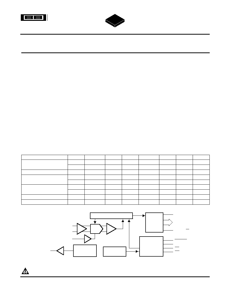
CDAC
_
+
Output
Latches
and
3-State
Drivers
BYTE
16-/8-Bit
Parallel DATA
Output Bus
SAR
Conversion
and
Control Logic
Comparator
Clock
+IN
-IN
REFIN
CONVST
BUSY
CS
RD
4.096-V
Internal
Reference
REFOUT
BUS 18/16
ADS8481
SLAS385A ≠ FEBRUARY 2006 ≠ REVISED MARCH 2006
18-BIT, 1-MSPS, PSEUDO-DIFFERENTIAL UNIPOLAR INPUT, MICROPOWER SAMPLING
ANALOG-TO-DIGITAL CONVERTER WITH PARALLEL INTERFACE AND REFERENCE
∑
Medical Instruments
∑
0 to 1 MSPS Sampling Rate
∑
Optical Networking
∑
18-Bit NMC Ensured Over Temperature
∑
Transducer Interface
∑
Low ±0.1 mV Offset Error
∑
High Accuracy Data Acquisition Systems
∑
Low 0.2 ppm/∞C Offset Error Temperature
∑
Magnetometers
Drift
∑
Low 0.6 ppm/∞C Gain Error Temperature Drift
∑
Zero Latency
The ADS8481 is an 18-bit, 1-MSPS A/D converter
∑
Low Power: 220 mW at 1 MSPS
with
an
internal
4.096-V
reference
and
a
∑
Unipolar Single-Ended Input Range: 0 V to
pseudo-differential unipolar single-ended input. The
V
ref
device includes a 18-bit capacitor-based SAR A/D
converter with inherent sample and hold. The
∑
Onboard Reference
ADS8481 offers a full 18-bit interface, a 16-bit option
∑
Onboard Reference Buffer
where data is read using two read cycles, or an 8-bit
∑
High-Speed Parallel Interface
bus option using three read cycles.
∑
Wide Digital Supply 2.7 V ~ 5.25 V
The ADS8481 is available in a 7x7 QFN package
∑
8-/16-/18-Bit Bus Transfer
and is characterized over the industrial ≠40∞C to
85∞C temperature range.
∑
7x7 QFN Package
HIGH SPEED SAR CONVERTER FAMILY
TYPE/SPEED
500 kHz
580 kHz
750 kHz
1 MHz
1.25 MHz
2 MHz
3 MHz
4MHz
ADS8383
ADS8381
ADS8481
18-Bit Pseudo-Diff
ADS8380(S)
18-Bit Pseudo-Bipolar, Fully Diff
ADS8382(S)
ADS8482
ADS8371
ADS8471
ADS8401
ADS8411
16-Bit Pseudo-Diff
ADS8405
ADS8472
ADS8402
ADS8412
16-Bit Pseudo-Bipolar, Fully Diff
ADS8406
14-Bit Pseudo-Diff
ADS7890 (s)
ADS7891
12-Bit Pseudo-Diff
ADS7886
ADS7883
ADS7881
Please be aware that an important notice concerning availability, standard warranty, and use in critical applications of Texas
Instruments semiconductor products and disclaimers thereto appears at the end of this data sheet.
PRODUCTION DATA information is current as of publication date.
Copyright © 2006, Texas Instruments Incorporated
Products conform to specifications per the terms of the Texas
Instruments standard warranty. Production processing does not
necessarily include testing of all parameters.
www.ti.com
ABSOLUTE MAXIMUM RATINGS
(1)
ADS8481
SLAS385A ≠ FEBRUARY 2006 ≠ REVISED MARCH 2006
These devices have limited built-in ESD protection. The leads should be shorted together or the device placed in conductive foam
during storage or handling to prevent electrostatic damage to the MOS gates.
ORDERING INFORMATION
(1)
MAXIMUM
MAXIMUM
NO MISSING
TRANS-
TEMPER-
INTEGRAL
DIFFERENTIAL
CODES
PACKAGE
PACKAGE
ORDERING
PORT
MODEL
ATURE
LINEARITY
LINEARITY (LSB)
RESOLUTION
TYPE
DESIGNATOR
INFORMATION
MEDIA
RANGE
(LSB)
(BIT)
QTY.
ADS8482IRGZT
Tape and
reel 250
7x7 48 Pin
≠40∞C to
ADS8481I
±5
≠1 to +2.5
18
RGZ
QFN
85∞C
ADS8481IRGZR
Tape and
reel 1000
ADS8481IBRGZT
Tape and
reel 250
7x7 48 Pin
≠40∞C to
ADS8481IB
±3.5
≠1 to +1.5
18
RGZ
QFN
85∞C
ADS8481IBRGZR
Tape and
reel 1000
(1)
For the most current specifications and package information, refer to our website at
www.ti.com
.
over operating free-air temperature range (unless otherwise noted)
VALUE
UNIT
+IN to AGND
≠0.4 to +VA + 0.1
V
≠IN to AGND
≠0.4 to 0.5
V
Voltage
+VA to AGND
≠0.3 to 7
V
+VBD to BDGND
≠0.3 to 7
V
+VA to +VBD
≠0.3 to 2.55
V
Digital input voltage to BDGND
≠0.3 to +VBD + 0.3
V
Digital output voltage to BDGND
≠0.3 to +VBD + 0.3
V
T
A
Operating free-air temperature range
≠40 to 85
∞C
T
stg
Storage temperature range
≠65 to 150
∞C
Junction temperature (T
J
max)
150
∞C
Power dissipation
(T
J
Max ≠ T
A
)/
JA
QFN package
JA
thermal impedance
22
∞C/W
Vapor phase (60 sec)
215
∞C
Lead temperature, soldering
Infrared (15 sec)
220
∞C
(1)
Stresses beyond those listed under absolute maximum ratings may cause permanent damage to the device. These are stress ratings
only, and functional operation of the device at these or any other conditions beyond those indicated under recommended operating
conditions is not implied. Exposure to absolute-maximum-rated conditions for extended periods may affect device reliability.
2
Submit Documentation Feedback
www.ti.com
SPECIFICATIONS
ADS8481
SLAS385A ≠ FEBRUARY 2006 ≠ REVISED MARCH 2006
T
A
= ≠40∞C to 85∞C, +VA = 5 V, +VBD = 3 V or 5 V, V
ref
= 4.096 V, f
SAMPLE
= 1 MSPS (unless otherwise noted)
PARAMETER
TEST CONDITIONS
MIN
TYP
MAX
UNIT
ANALOG INPUT
Full-scale input voltage
(1)
+IN ≠ (≠IN)
0
V
ref
V
+IN
≠0.2
V
ref
+0.2
Absolute input voltage
V
≠IN
≠0.2
0.2
Input capacitance
65
pF
Input leakage current
1
nA
SYSTEM PERFORMANCE
Resolution
18
Bits
ADS8481I
18
18
No missing codes
Bits
ADS8481IB
18
ADS8481I
≠5 ≠1.5/+1.9
5
LSB
Integral linearity
(2) (3)
(18 bit)
ADS8481IB
≠3.5 ≠1.5/+1.9
3.5
ADS8481I
≠1 ≠0.5/+0.7
2.5
LSB
Differential linearity
(18 bit)
ADS8481IB
≠1 ≠0.5/+0.7
1.5
ADS8481I
≠0.5
±0.1
0.5
Offset error
(4)
mV
ADS8481IB
≠0.5
±0.1
0.5
Offset error temperature drift
±0.2
ppm/∞C
ADS8481I
V
ref
= 4.096 V
≠0.075
±0.05
0.075
%FS
Gain error
(4) (5)
ADS8481IB
V
ref
= 4.096 V
≠0.075
±0.05
0.075
%FS
Gain error temperature drift
±0.6
ppm/∞C
Noise
30
µ
V RMS
Power supply rejection ratio
At 3FFFFh output code
60
dB
SAMPLING DYNAMICS
Conversion time
650
710
ns
Acquisition time
250
ns
Throughput rate
1
MHz
Aperture delay
4
ns
Aperture jitter
5
ps
Step response
150
ns
Over voltage recovery
150
ns
(1)
Ideal input span, does not include gain or offset error.
(2)
LSB means least significant bit
(3)
This is endpoint INL, not best fit.
(4)
Measured relative to an ideal full-scale input [+IN ≠ (≠IN)] of 4.096 V
(5)
This specification does not include the internal reference voltage error and drift.
3
Submit Documentation Feedback
www.ti.com
SPECIFICATIONS (Continued)
ADS8481
SLAS385A ≠ FEBRUARY 2006 ≠ REVISED MARCH 2006
T
A
= ≠40∞C to 85∞C, +VA = 5 V, +VBD = 3 V or 5 V, V
ref
= 4.096 V, f
SAMPLE
= 1 MSPS (unless otherwise noted)
PARAMETER
TEST CONDITIONS
MIN
TYP
MAX
UNIT
DYNAMIC CHARACTERISTICS
ADS8481I
≠110
V
IN
= 4 V
pp
at 1 kHz
ADS8481IB
≠112
ADS8481I
≠106
Total harmonic distortion (THD)
(1)
V
IN
= 4 V
pp
at 10 kHz
dB
ADS8481IB
≠108
ADS8481I
≠98
V
IN
= 4 V
pp
at 100 kHz
ADS8481IB
≠99
ADS8481I
92
V
IN
= 4 V
pp
at 1 kHz
ADS8481IB
94
ADS8481I
91
Signal to noise ratio (SNR)
(1)
V
IN
= 4 V
pp
at 10 kHz
dB
ADS8481IB
93
ADS8481I
90
V
IN
= 4 V
pp
at 100 kHz
ADS8481IB
92
ADS8481I
91
V
IN
= 4 V
pp
at 1 kHz
ADS8481IB
93
ADS8481I
90
Signal to noise + distortion (SINAD)
(1)
V
IN
= 4 V
pp
at 10 kHz
dB
ADS8481IB
92
ADS8481I
89
V
IN
= 4 V
pp
at 100 kHz
ADS8481IB
91
ADS8481I
110
V
IN
= 4 V
pp
at 1 kHz
ADS8481IB
112
ADS8481I
108
Spurious free dynamic range (SFDR)
(1)
V
IN
= 4 V
pp
at 10 kHz
dB
ADS8481IB
107
ADS8481I
98
V
IN
= 4 V
pp
at 100 kHz
ADS8481IB
98
≠3dB Small signal bandwidth
15
MHz
VOLTAGE REFERENCE INPUT
Reference voltage at REFIN, Vref
3.0
4.096
4.2
V
Reference resistance
(2)
500
k
Reference current drain
f
s
= 1 MHz
1
mA
(1)
Calculated on the first nine harmonics of the input frequency.
(2)
Can vary ±20%
4
Submit Documentation Feedback
www.ti.com
SPECIFICATIONS (Continued)
ADS8481
SLAS385A ≠ FEBRUARY 2006 ≠ REVISED MARCH 2006
T
A
= ≠40∞C to 85∞C, +VA = 5 V, +VBD = 3 V or 5 V, V
ref
= 4.096 V, f
SAMPLE
= 1 MSPS (unless otherwise noted)
PARAMETER
TEST CONDITIONS
MIN
TYP
MAX
UNIT
INTERNAL REFERENCE OUTPUT
Internal reference start-up time
From 95% (+VA), with 1-
µ
F storage capacitor
120
ms
Reference voltage range, V
ref
I
O
= 0 A
4.081
4.096
4.111
V
Source current
Static load
10
µ
A
Line regulation
+VA = 4.75 V to 5.25 V
60
µ
V
Drift
I
O
= 0 A
±6
PPM/C
DIGITAL INPUT/OUTPUT
Logic family ≠ CMOS
V
IH
I
IH
= 5
µ
A
+VBD≠1
+V
BD
+0.3
V
IL
I
IL
= 5
µ
A
≠0.3
0.8
Logic level
V
V
OH
I
OH
= 2 TTL loads
+V
BD
≠ 0.6
V
OL
I
OL
= 2 TTL loads
0.4
Data format ≠ Straight Binary
POWER SUPPLY REQUIREMENTS
+VBD
2.7
3.3
5.25
V
Power supply
voltage
+VA
4.75
5
5.25
V
Supply current
(1)
f
s
= 1 MHz
44
48
mA
Power dissipation
(1)
f
s
= 1 MHz
220
240
mW
TEMPERATURE RANGE
Operating free-air
≠40
85
∞C
(1)
This includes only +VA current. +VBD current is typical 1 mA with 5 pF load capacitance on all output pins.
5
Submit Documentation Feedback