Burr Brown Products
from Texas Instruments
FEATURES
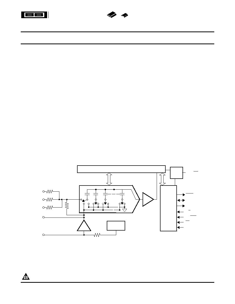
DESCRIPTION
APPLICATIONS
Successive Approximation Register
Clock
Comparator
CS
CDAC
Buffer
REF
CAP
R1
IN
10 k
4.9 k
Internal
+2.5 V Ref
4 k
Serial
Data
Out
&
Control
BUSY
DATACLK
DATA
2.5 k
9.8 k
R2
IN
R3
IN
EXT/INT
R/C
SB/BTC
PWRD
ADS8509
SLAS324A ≠ OCTOBER 2004 ≠ REVISED JUNE 2005
16-BIT 250-KSPS SERIAL CMOS SAMPLING ANALOG-TO-DIGITAL CONVERTER
∑
250-kHz Sampling Rate
The
ADS8509
is
a
complete
16-bit
sampling
analog-to-digital (A/D) converter using state-of-the-art
∑
4-V, 5-V, 10 V, ±3.33-V, ±5-V, and ±10-V Input
CMOS structures. It contains a complete 16-bit,
Ranges
capacitor-based, successive approximation register
∑
±2.0 LSB Max INL
(SAR) A/D converter with sample-and-hold, refer-
∑
±1 LSB Max DNL, 16-Bit No Missing Codes
ence, clock, and a serial data interface. Data can be
output
using
the
internal
clock
or
can
be
∑
SPI Compatible Serial Output with
synchronized to an external data clock. The ADS8509
Daisy-Chain (TAG) Feature
also provides an output synchronization pulse for
∑
Single 5-V Supply
ease of use with standard DSP processors.
∑
Pin-Compatible With ADS7809 (Low Speed)
The ADS8509 is specified at a 250-kHz sampling rate
and 12-Bit ADS8508/7808
over the full temperature range. Precision resistors
∑
Uses Internal or External Reference
provide various input ranges including ±10 V and 0 V
∑
70-mW Typ Power Dissipation at 250 KSPS
to 5 V, while the innovative design allows operation
from a single +5-V supply with power dissipation
∑
20-Pin SO and 28-Pin SSOP Packages
under 100 mW.
∑
Simple DSP Interface
The ADS8509 is available in 20-pin SO and 28-pin
SSOP packages, both fully specified for operation
over the industrial -40∞C to 85∞C temperature range.
∑
Industrial Process Control
∑
Data Acquisition Systems
∑
Digital Signal Processing
∑
Medical Equipment
∑
Instrumentation
Please be aware that an important notice concerning availability, standard warranty, and use in critical applications of Texas
Instruments semiconductor products and disclaimers thereto appears at the end of this data sheet.
PRODUCTION DATA information is current as of publication date.
Copyright © 2004≠2005, Texas Instruments Incorporated
Products conform to specifications per the terms of the Texas
Instruments standard warranty. Production processing does not
necessarily include testing of all parameters.
www.ti.com
ABSOLUTE MAXIMUM RATINGS
ADS8509
SLAS324A ≠ OCTOBER 2004 ≠ REVISED JUNE 2005
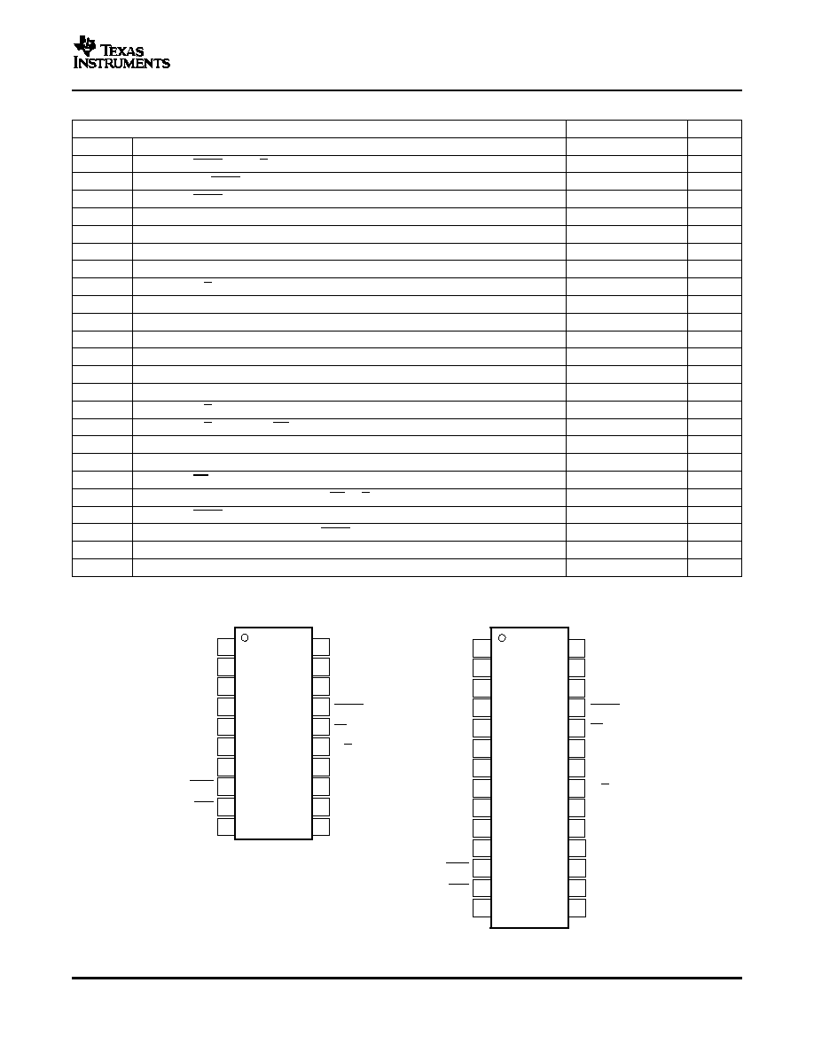
PACKAGE/ORDERING INFORMATION
(1)
MINIMUM
NO
MINIMUM
SPECIFICATION
RELATIVE
PACKAGE
PACKAGE
ORDERING
TRANSPORT
PRODUCT
MISSING
SINAD
TEMPERATURE
ACCURACY
LEAD
DESIGNATOR
NUMBER
MEDIA, QTY
CODE
(dB)
RANGE
(LSB)
ADS8509IBDW
Tube, 25
SO-20
DW
ADS8509IBDWR
Tape and Reel, 2000
ADS8509IB
±2
16
85
-40∞C to 85∞C
ADS8509IBDB
Tube, 50
SSOP-28
DB
ADS8509IBDBR
Tape and Reel, 2000
ADS8509IDW
Tube, 25
SO-20
DW
ADS8509IDWR
Tape and Reel, 2000
ADS8509I
±3
15
83
-40∞C to 85∞C
ADS8509IDB
Tube, 50
SSOP-28
DB
ADS8509IDBR
Tape and Reel, 2000
(1)
For the most current package and ordering information, see the Package Option Addendum at the end of this document, or see the TI
website at www.ti.com.
over operating free-air temperature range (unless otherwise noted)
(1)
UNIT
R1
IN
±25 V
R2
IN
±25 V
Analog inputs
R3
IN
±25 V
REF
+V
ANA
+ 0.3 V to AGND2 - 0.3 V
DGND, AGND2
±0.3 V
V
ANA
6 V
Ground voltage differences
V
DIG
to V
ANA
0.3 V
V
DIG
6 V
Digital inputs
-0.3 V to +V
DIG
+ 0.3 V
Maximum junction temperature
165∞C
Storage temperature range
≠65
∞
C to 150
∞
C
Internal power dissipation
700 mW
Lead temperature (soldering, 1.6 mm from case 10 seconds)
260∞C
(1)
All voltage values are with respect to network ground terminal.
2
www.ti.com
ELECTRICAL CHARACTERISTICS
ADS8509
SLAS324A ≠ OCTOBER 2004 ≠ REVISED JUNE 2005
At T
A
= -40∞C to 85∞C, f
s
= 250 kHz, V
DIG
= V
ANA
= 5 V, using internal reference and 0.1%, 0.25 W fixed resistors (See
Figure 29
and
Figure 30
) (unless otherwise specified)
ADS8509I
ADS8509IB
PARAMETER
TEST CONDITIONS
UNIT
MIN
TYP
MAX
MIN
TYP
MAX
Resolution
16
16
Bits
ANALOG INPUT
Voltage ranges
(1)
Impedance
(1)
Capacitance
50
50
pF
THROUGHPUT SPEED
Conversion cycle
Acquire and convert
4
4
µs
Throughput rate
250
250
kHz
DC ACCURACY
INL
Integral linearity error
-3
3
-2
2
LSB
(2)
DNL
Differential linearity error
-2
2
-1
1
LSB
No missing codes
15
16
Bits
Transition noise
(3)
1
1
LSB
±10 V range
Int. Ref. with 0.1% external
-0.5
0.5
-0.5
0.5
Full-scale
%FSR
fixed resistors
error
(4) (5)
All other ranges
-0.5
0.5
-0.5
0.5
Full-scale error drift
Int. Ref.
±7
±7
ppm/∞C
±10 V range
Ext. Ref. with 0.1% external
-0.5
0.5
-0.5
0.5
Full-scale
%FSR
fixed resistors
error
(4) (5)
All other ranges
-0.5
0.5
-0.5
0.5
Full-scale error drift
Ext. Ref.
±2
±2
ppm/∞C
Bipolar zero error
(4)
-10
10
-5
5
mV
Bipolar zero error drift
±0.4
±0.4
ppm/∞C
10 V range
-5
5
-5
5
Unipolar zero
mV
4 V and 5 V
-3
3
-3
3
error
(4)
range
Unipolar zero error drift
±2
±2
ppm/∞C
Recovery to rated accuracy after
1-µF Capacitor to CAP
1
1
ms
power down
Power supply sensitivity
-8
8
-8
8
+4.75 V < V
D
< +5.25 V
LSB
(V
DIG
= V
ANA
= V
D
)
AC ACCURACY
SFDR
Spurious-free dynamic range
f
I
= 20 kHz
90
99
95
99
dB
(6)
THD
Total harmonic distortion
f
I
= 20 kHz
-98
-90
-98
-93
dB
SINAD
f
I
= 20 kHz
83
88
85
88
dB
Signal-to-(noise+distortion)
≠60-dB Input
30
32
dB
SNR
Signal-to-noise ratio
f
I
= 20 kHz
83
88
86
88
dB
Full-power bandwidth
(7)
500
500
kHz
SAMPLING DYNAMICS
Aperture delay
5
5
ns
Transient response
FS Step
2
2
µs
Overvoltage recovery
(8)
150
150
ns
(1)
±10 V, 0 V to 5 V, etc. (see
Table 3
)
(2)
LSB means least significant bit. For the ±10-V input range, one LSB is 305 µV.
(3)
Typical rms noise at worst case transitions and temperatures.
(4)
As measured with fixed resistors shown in
Figure 29
and
Figure 30
. Adjustable to zero with external potentiometer. Factory calibrated
with 0.1%, 0.25 W resistors.
(5)
For bipolar input ranges, full-scale error is the worst case of -full-scale or +full-scale uncalibrated deviation from ideal first and last code
transitions, divided by the transition voltage (not divided by the full-scale range) and includes the effect of offset error. For unipolar input
ranges, full-scale error is the deviation of the last code transition divided by the transition voltage. It also includes the effect of offset
error.
(6)
All specifications in dB are referred to a full-scale ±10-V input.
(7)
Full-power bandwidth is defined as the full-scale input frequency at which signal-to-(noise + distortion) degrades to 60 dB.
(8)
Recovers to specified performance after 2 x FS input overvoltage.
3
www.ti.com
ADS8509
SLAS324A ≠ OCTOBER 2004 ≠ REVISED JUNE 2005
ELECTRICAL CHARACTERISTICS (continued)
At T
A
= -40∞C to 85∞C, f
s
= 250 kHz, V
DIG
= V
ANA
= 5 V, using internal reference and 0.1%, 0.25 W fixed resistors (See
Figure 29
and
Figure 30
) (unless otherwise specified)
ADS8509I
ADS8509IB
PARAMETER
TEST CONDITIONS
UNIT
MIN
TYP
MAX
MIN
TYP
MAX
REFERENCE
Internal reference voltage
No load
2.48
2.5
2.52
2.48
2.5
2.52
V
Internal reference source current
1
1
µA
(must use external buffer)
Internal reference drift
8
8
ppm/∞C
External reference voltage range
2.3
2.5
2.7
2.3
2.5
2.7
V
for specified linearity
External reference current drain
Ext. 2.5-V Ref.
100
100
µA
DIGITAL INPUTS
Logic levels
V
IL
Low-level input voltage
-0.3
0.8
-0.3
0.8
V
V
IH
High-level input voltage
2.0
V
DIG
+0.3 V
2.0
V
DIG
+0.3 V
V
I
IL
Low-level input current
V
IL
= 0 V
±10
±10
µA
I
IH
High-level input current
V
IH
= 5 V
±10
±10
µA
DIGITAL OUTPUTS
Data format (Serial 16-bits)
Data coding (Binary 2's comp-
lement or straight binary)
Pipeline delay (Conversion re-
sults only available after com-
pleted conversion.)
Data clock (Selectable for
internal or external data clock)
Internal clock (output only when
EXT/INT Low
9
9
MHz
transmitting data)
External clock (can run continu-
EXT/INT High
0.1
26
0.1
26
ally but not recommended for
MHz
optimum performance)
V
OL
Low-level output voltage
I
SINK
= 1.6 mA
0.4
0.4
V
V
OH
High-level output voltage
I
SOURCE
= 500 µA
4
4
V
Leakage current
Hi-Z state,
±5
±5
µA
V
OUT
= 0 V to V
DIG
Output capacitance
Hi-Z state
15
15
pF
POWER SUPPLIES
V
DIG
Digital input voltage
4.75
5
5.25
4.75
5
5.25
V
V
ANA
Analog input voltage
4.75
5
5.25
4.75
5
5.25
V
Must be
V
ANA
I
DIG
Digital input current
4
4
mA
I
ANA
Analog input current
10
10
mA
POWER DISSIPATION
PWRD Low
f
S
= 250 kHz
70
100
70
100
mW
PWRD High
50
50
µW
TEMPERATURE RANGE
Specified performance
-40
85
-40
85
∞C
Derated performance
(9)
-55
125
-55
125
∞C
Storage
-65
150
-65
150
∞C
THERMAL RESISTANCE (
JA
)
SSOP
62
62
∞C/W
SO
46
46
∞C/W
(9)
The internal reference may not be started correctly beyond the industrial temperature range (-40∞C to 85∞C), therefore use of an
external reference is recommended.
4
www.ti.com
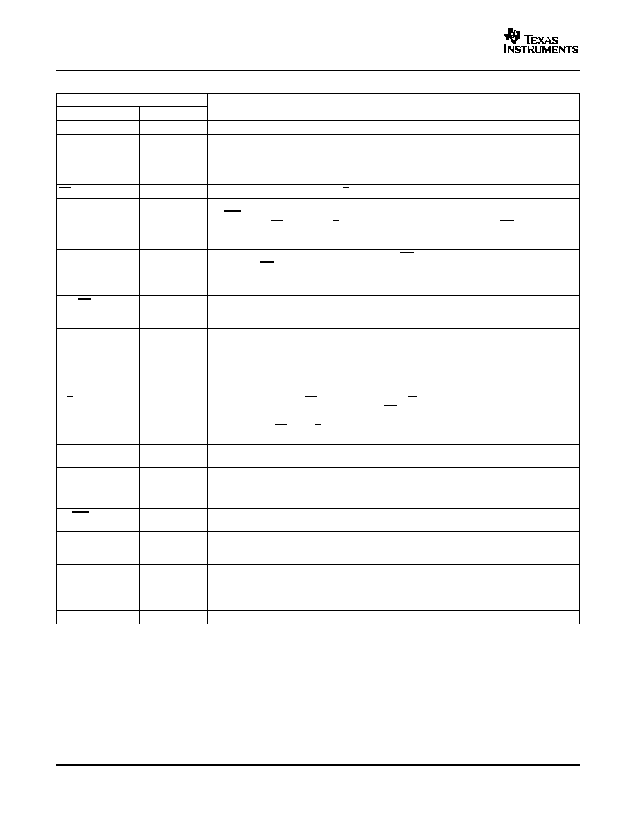
TIMING REQUIREMENTS, T
A
= ≠40∞C to 85∞C
VDIG
VANA
BUSY
CS
R/C
TAG
DATA
DATACLK
SYNC
R1IN
AGND1
REF
CAP
AGND2
1
2
3
4
5
6
7
8
9
10
20
19
18
17
16
15
14
13
12
11
DW PACKAGE
R2IN
R3IN
SB/BTC
EXT/INT
DGND
PWRD
VDIG
VANA
BUSY
CS
R/C
NC
TAG
NC
DATA
DATACLK
SYNC
R1IN
AGND1
NC
CAP
AGND2
NC
NC
NC
REF
DGND
1
2
3
4
5
6
7
8
9
10
11
12
13
14
28
27
26
25
24
23
22
21
20
19
18
17
16
15
DB PACKAGE
R2IN
SB/BTC
EXT/INT
PWRD
NC
(TOP VIEW)
(TOP VIEW)
NC
R3IN
ADS8509
SLAS324A ≠ OCTOBER 2004 ≠ REVISED JUNE 2005
PARAMETER
MIN
TYP
MAX
UNIT
t
w1
Pulse duration, convert
40
ns
t
d1
Delay time, BUSY from R/C low
6
20
ns
t
w2
Pulse duration, BUSY low
2.2
µs
t
d2
Delay time, BUSY, after end of conversion
5
ns
t
d3
Delay time, aperture
5
ns
t
conv
Conversion time
2.2
µs
t
acq
Acquisition time
1.8
µs
t
conv
+ t
acq
Cycle time
4
µs
t
d4
Delay time, R/C Low to internal DATACLK output
270
ns
t
c1
Cycle time, internal DATACLK
110
ns
t
d5
Delay time, data valid to internal DATACLK high
15
35
ns
t
d6
Delay time, data valid after internal DATACLK low
20
35
ns
t
c2
Cycle time, external DATACLK
35
ns
t
w3
Pulse duration, external DATACLK high
15
ns
t
w4
Pulse duration, external DATACLK low
15
ns
t
su1
Setup time, R/C rise/fall to external DATACLK high
15
t
C2
+ 5
ns
t
su2
Setup time, R/C transition to CS transition
10
ns
t
d7
Delay time, SYNC, after external DATACLK high
3
35
ns
t
d8
Delay time, data valid
2
20
ns
t
d9
Delay time, CS to rising edge
10
ns
t
d10
Delay time, previous data available after CS, R/C low
2
µs
t
su3
Setup time, BUSY transition to first external DATACLK
5
ns
t
d11
Delay time, final external DATACLK to BUSY falling edge
1
µs
t
su3
Setup time, TAG valid
0
ns
t
h1
Hold time, TAG valid
2
ns
5
www.ti.com
ADS8509
SLAS324A ≠ OCTOBER 2004 ≠ REVISED JUNE 2005
Terminal Functions
TERMINAL
DESCRIPTION
NAME
DB NO.
DW NO.
I/O
AGND1
2
2
≠
Analog ground. Used internally as ground reference point. Minimal current flow.
AGND2
9
7
≠
Analog ground
BUSY
25
17
O
Busy output. Falls when a conversion is started, and remains low until the conversion is completed
and the data is latched into the output shift register.
CAP
6
5
≠
Reference buffer capacitor. 2.2-µF Tantalum to ground.
CS
24
16
≠
Chip select. Internally ORed with R/C.
DATA
17
13
O
Serial data output. Data is synchronized to DATACLK, with the format determined by the level of
SB/BTC. In the external clock mode, after 16 bits of data, the ADS8509 outputs the level input on
TAG as long as CS is low and R/C is high (see
Figure 8
and
Figure 9
). If EXT/INT is low, data is
valid on both the rising and falling edges of DATACLK, and between conversions DATA stays at
the level of the TAG input when the conversion was started.
DATACLK
16
12
I/O
Either an input or an output depending on the EXT/INT level. Output data is synchronized to this
clock. If EXT/INT is low, DATACLK transmits 16 pulses after each conversion, and then remains
low between conversions.
DGND
14
10
≠
Digital ground
EXT/INT
13
9
≠
Selects external or internal clock for transmitting data. If high, data is output synchronized to the
clock input on DATACLK. If low, a convert command initiates the transmission of the data from the
previous conversion, along with 16-clock pulses output on DATACLK.
NC
5, 8, 10,
≠
≠
No connect
11, 18,
20, 22,
23
PWRD
26
18
I
Power down input. If high, conversions are inhibited and power consumption is significantly
reduced. Results from the previous conversion are maintained in the output shift register.
R/C
21
15
I
Read/convert input. With CS low, a falling edge on R/C puts the internal sample-and-hold into the
hold state and starts a conversion. When EXT/INT is low, this also initiates the transmission of the
data results from the previous conversion. If EXT/INT is high, a rising edge on R/C with CS low, or
a falling edge on CS with R/C high, transmits a pulse on SYNC and initiates the transmission of
data from the previous conversion.
REF
7
6
I/O
Reference input/output. Outputs internal 2.5-V reference. Can also be driven by external system
reference. In both cases, bypass to ground with a 2.2-µF tantalum capacitor.
R1
IN
1
1
I
Analog input. See
Table 3
for input range connections.
R2
IN
3
3
I
Analog input. See
Table 3
for input range connections.
R3
IN
4
4
I
Analog input. See
Table 3
for input range connections.
SB/BTC
12
8
O
Select straight binary or binary 2's complement data output format. If high, data is output in a
straight binary format. If low, data is output in a binary 2's complement format.
SYNC
15
11
O
Sync output. This pin is used to supply a data synchronization pulse when the EXT level is high
and at least one external clock pulse has occured when not in the read mode. See the external
clock modes desciptions.
TAG
19
14
I
Tag input for use in the external clock mode. If EXT is high, digital data input from TAG is output
on DATA with a delay that is dependent on the external clock mode. See
Figure 8
and
Figure 9
.
V
ANA
27
19
I
Analog supply input. Nominally +5 V. Connect directly to pin 20, and decouple to ground with
0.1-µF ceramic and 10-µF tantalum capacitors.
V
DIG
28
20
I
Digital supply input. Nominally +5 V. Connect directly to pin 19. Must be
V
ANA
.
6
www.ti.com
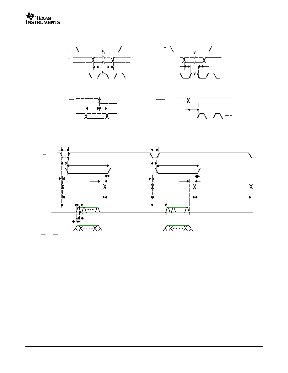
PARAMETER MEASUREMENT INFORMATION
1
2
t
su1
t
su1
CS
R/C
External
DATACLK
CS Set Low, Discontinuous Ext DATACLK
t
su1
t
su1
R/C
CS
External
DATACLK
R/C Set Low, Discontinuous Ext DATACLK
t
su2
t
su2
CS
R/C
t
su3
BUSY
External
DATACLK
CS Set Low, Discontinuous Ext DATACLK
R/C
BUSY
STATUS
(N+1)th Accquisition
(N+1)th Conversion
Error
Correction
Nth Conversion
Error
Correction
Internal
DATACLK
(N-1)th Conversion Data
DATA
Nth Conversion Data
(N+2)th Accquisition
1
2
16
2
16
D15
D0
D15
D0
TAG = 0
TAG = 0
TAG = 0
8 starts READ
CS, EXT/INT, and TAG are tied low
t
w1
t
d1
t
w2
t
d3
t
d11
t
d2
t
d3
t
w1
t
d1
t
w2
t
d11
t
d2
t
conv
t
acq
t
conv
t
acq
t
d4
t
d4
t
c1
t
d5
t
d6
1
ADS8509
SLAS324A ≠ OCTOBER 2004 ≠ REVISED JUNE 2005
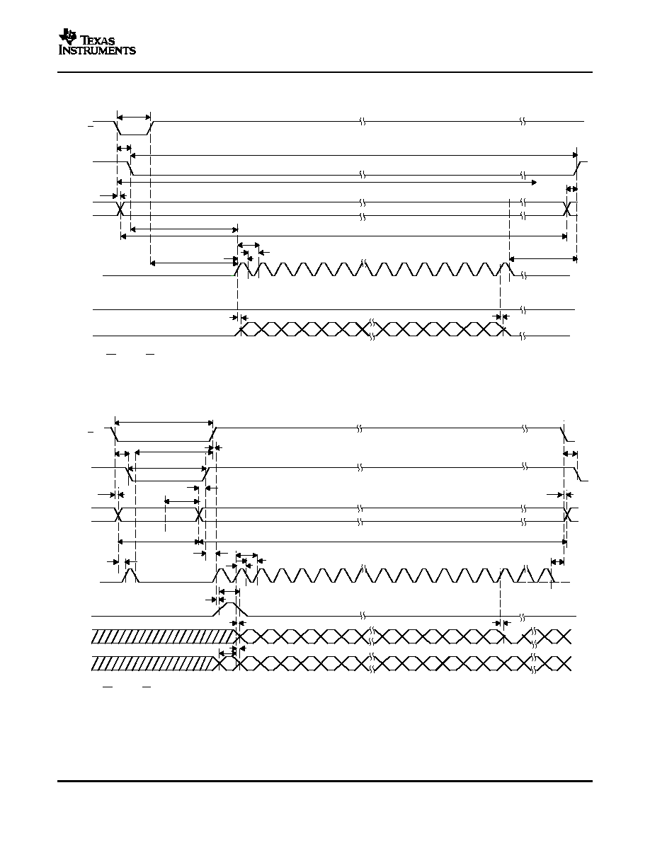
Figure 1. Critical Timing
Figure 2. Basic Conversion Timing - Internal DATACLK (Read Previous Data During Conversion)
7
www.ti.com
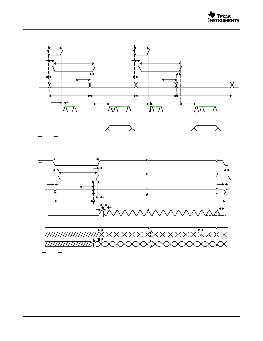
BUSY
STATUS
(N+1)th Accquisition
(N+1)th Conversion
Error
Correction
Nth Conversion
Error
Correction
External
DATACLK
DATA
Nth Data
(N+1)th Data
(N+2)th Accquisition
TAG = 0
No more
data to
shift out
No more
data to
shift out
TAG = 0
TAG = 0
TAG = 0
TAG = 0
R/C
EXT/INT tied high, CS and TAG are tied low
t
w1
+ t
su1
starts READ
t
w1
t
w1
t
d1
t
w2
t
d1
t
w2
t
d3
t
d11
t
d2
t
d3
t
d11
t
d2
t
su1
t
conv
t
acq
t
conv
t
acq
t
su3
t
su1
t
su3
1
16
1
2
16
1
16
1
2
16
BUSY
STATUS
(N+1) th Accquisition
Error
Correction
Nth Conversion
External
DATACLK
DATA
Nth Conversion Data
SYNC = 0
D15
0
1
2
3
15
14
16
TAG
T01
D05
D10
D12
D13
D14
T00
T04
T03
T02
T13
T12
T11
T06
T16
T15
T14
Tyy
5
4
11
12
13
10
D11
T05
D04
D03
D02
D01
Txx
T00
D00
Null
T17
Null
R/C
EXT/INT tied high, CS tied low
t
w1
+ t
su1
starts READ
t
w1
t
d1
t
w2
t
su1
t
d3
t
d11
t
d2
t
conv
t
acq
t
d3
t
d1
t
su3
t
w3
t
c2
t
w4
t
su1
t
d8
t
d8
t
su3
t
h1
ADS8509
SLAS324A ≠ OCTOBER 2004 ≠ REVISED JUNE 2005
PARAMETER MEASUREMENT INFORMATION (continued)
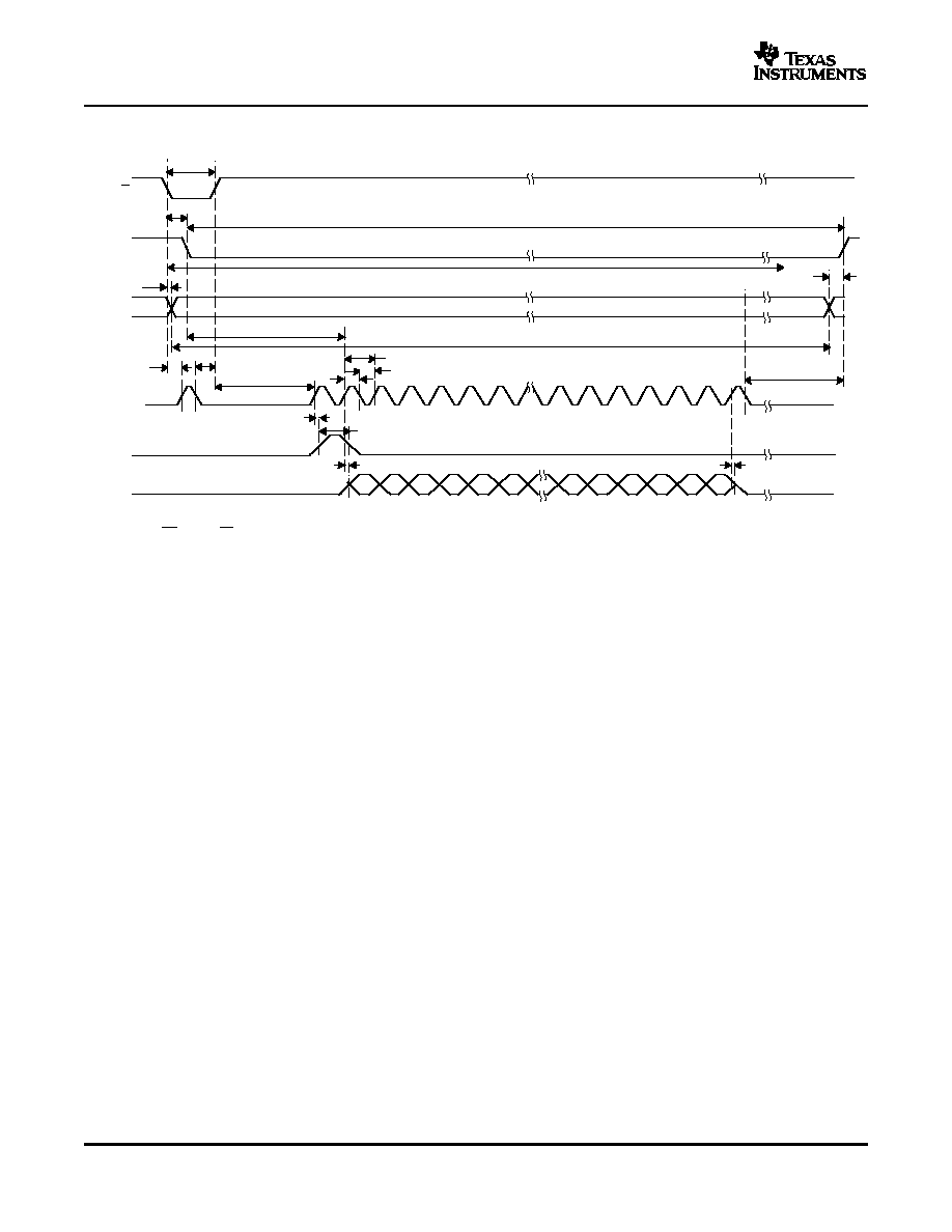
Figure 3. Basic Conversion Timing - External DATACLK
Figure 4. Read After Conversion (Discontinuous External DATACLK)
8
www.ti.com
BUSY
STATUS
Error
Correction
Nth Conversion
External
DATACLK
DATA
Nth Conversion Data
SYNC = 0
D15
0
1
2
3
15
14
16
D05
D10
D12
D13
D14
5
4
11
12
13
10
D11
D00
D04
D03
D02
D01
R/C
EXT/INT tied high, CS and TAG tied low
Rising DATACLK change DATA, t
w1
+ t
su1
Starts READ
TAG is not recommended for this mode. There is not enough
time to do so without violating t
d11
.
t
w1
t
d1
t
w2
t
d10
t
d3
t
su3
t
conv
t
d2
t
su1
t
w3
t
c2
t
w4
t
d11
t
d8
t
d8
BUSY
STATUS
(N+1)th Accquisition
Error
Correction
Nth Conversion
External
DATACLK
DATA
Nth Conversion Data
SYNC
D15
2
3
4
5
17
16
18
TAG
T01
D05
D10
D12
D13
D14
T00
T04
T03
T02
T13
T12
T11
T06
T16
T15
T14
Tyy
T17
7
6
13
14
15
12
D11
T05
D00
D04
D03
D02
D01
Txx
=0
0
1
T00
Null
R/C
EXT/INT tied high, CS tied low
t
w1
+ t
su1
starts READ
t
w1
t
su1
t
su1
t
d1
t
d1
t
d3
t
d11
t
d2
t
w2
t
d3
t
conv
t
acq
t
su1
t
su3
t
c2
t
w4
t
w3
t
c2
t
d7
t
d8
t
su3
t
h1
t
d8
t
su1
ADS8509
SLAS324A ≠ OCTOBER 2004 ≠ REVISED JUNE 2005
PARAMETER MEASUREMENT INFORMATION (continued)
Figure 5. Read During Conversion (Discontinuous External DATACLK)
Figure 6. Read After Conversion With SYNC (Discontinuous External DATACLK)
9
www.ti.com
BUSY
STATUS
Error
Correction
Nth Conversion
External
DATACLK
DATA
Nth Conversion Data
SYNC = 0
D15
2
3
4
5
17
16
18
D05
D10
D12
D13
D14
7
6
13
14
15
12
D11
D00
D04
D03
D02
D01
0
1
R/C
EXT/INT tied high, CS and TAG tied low
t
w1
+ t
su1
Starts READ
TAG is not recommended for this mode. There is not enough
time to do so without violating t
d11
.
t
w1
t
w2
t
d1
t
d3
t
d10
t
su3
t
su1
t
su1
t
w3
t
d7
t
c2
t
d8
t
c2
t
w4
t
su1
t
d8
t
d11
t
conv
t
d2
ADS8509
SLAS324A ≠ OCTOBER 2004 ≠ REVISED JUNE 2005
PARAMETER MEASUREMENT INFORMATION (continued)
Figure 7. Read During Conversion With SYNC (Discontinuous External DATACLK)
10
www.ti.com
0
1
2
3
4
17
18
Bit 15 (MSB)
Bit 14
Bit 1
Bit 0 (LSB)
T
ag 0
T
ag 1
T
ag 0
T
ag 1
T
ag 2
T
ag 15
T
ag 16
T
ag 17
T
ag 18
T
ag 19
t
c2
t
w4
t
w3
t
w1
t
su1
t
su2
t
d1
t su2
t
c2
t
d7
t
d8
t
d9
External
DA
T
ACLK
CS
R/C
BUSY
SYNC
DA
T
A
T
AG
ADS8509
SLAS324A ≠ OCTOBER 2004 ≠ REVISED JUNE 2005
PARAMETER MEASUREMENT INFORMATION (continued)
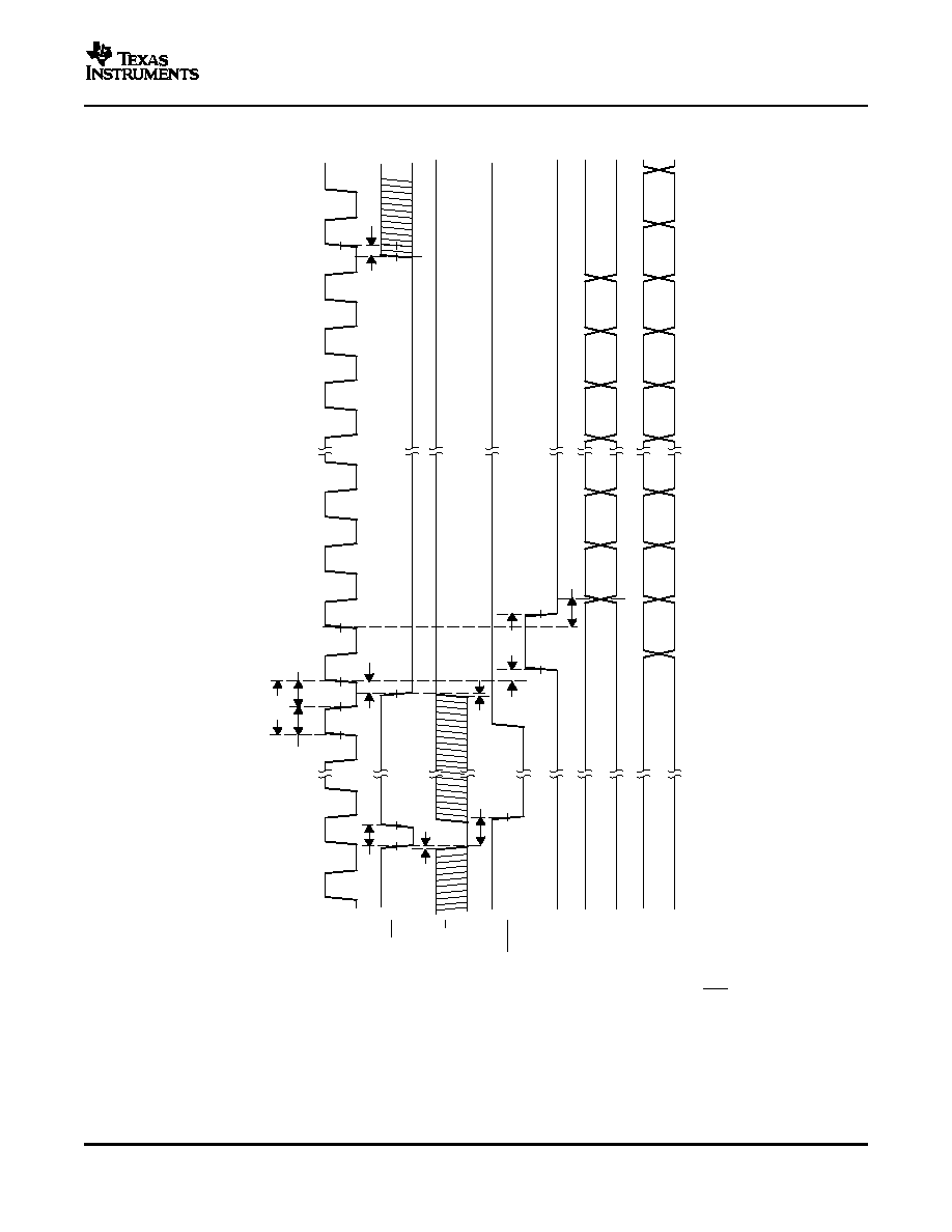
Figure 8. Conversion and Read Timing with Continuous External DATACLK (EXT/INT Tied High) Read
After Conversions (Not Recommended)
11
www.ti.com
t
c2
t
w4
t
w3
t
w1
t
su2
t
su1
t
d10
t
d8
t
d1
t
su1
t
c2
t
d8
External
DA
T
ACLK
CS
R/C
BUSY
SYNC
DA
T
A
T
AG
Bit 15 (MSB)
Bit 0 (LSB)
T
ag 0
T
ag 1
T
ag 0
T
ag 1
T
ag 16
T
ag 17
T
ag 18
T
ag 19
ADS8509
SLAS324A ≠ OCTOBER 2004 ≠ REVISED JUNE 2005
PARAMETER MEASUREMENT INFORMATION (continued)
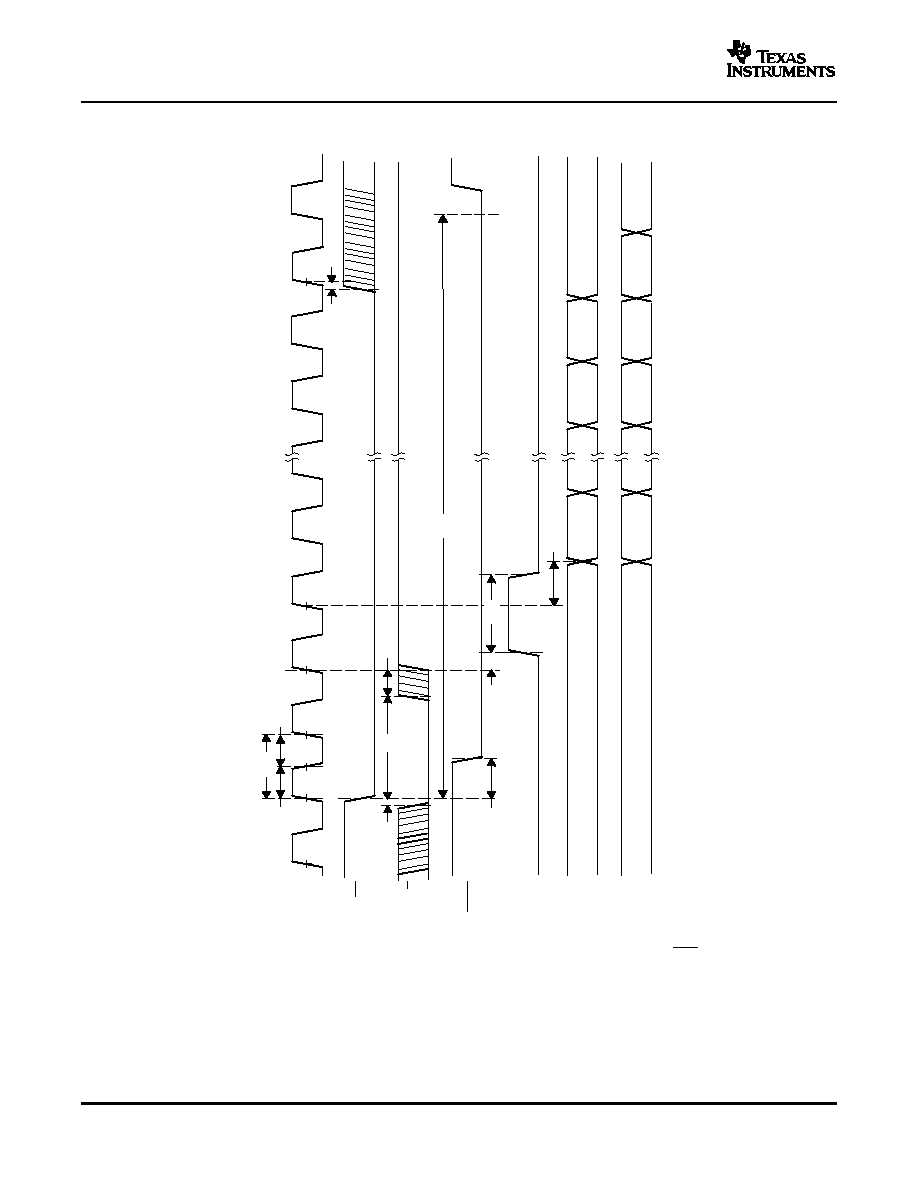
Figure 9. Conversion and Read Timing with Continous External DATACLK (EXT/INT Tied High) Read
Previous Conversion Results During Conversion (Not Recommended)
12
www.ti.com
TYPICAL CHARACTERISTICS
75
80
85
90
95
100
105
-40
25
85
SFDR - Spurious Free Dynamic Range - dB
T
A
- Free-Air Temperature -
5
C
f
s
= 250 KSPS,
f
i
= 20 kHz
-70
-75
-80
-85
-90
-95
-100
-40
25
85
THD - T
otal Harmonic Distortion - dB
T
A
- Free-Air Temperature -
5
C
f
s
= 250 KSPS,
f
i
= 20 kHz
SNR - Signal-to-Noise Ratio - dB
70
75
80
85
90
95
100
-40
25
85
T
A
- Free-Air Temperature -
5
C
f
s
= 250 KSPS,
f
i
= 20 kHz
70
75
80
85
90
95
100
-40
25
85
SINAD - Signal-T
o-Noise and Distortion - dB
T
A
- Free-Air Temperature -
5
C
f
s
= 250 KSPS,
f
i
= 20 kHz
SINAD - Signal-T
o-Noise and Distortion - dB
65
70
75
80
85
90
1
10
100
f
i
- Input Frequency - kHz
65
70
75
80
85
90
1
10
100
SNR - Signal-to-Noise Ratio - dB
f
i
- Input Frequency - kHz
ADS8509
SLAS324A ≠ OCTOBER 2004 ≠ REVISED JUNE 2005
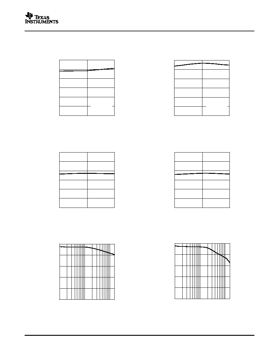
SPURIOUS FREE DYNAMIC RANGE
TOTAL HARMONIC DISTORTION
vs
vs
FREE-AIR TEMPERATURE
FREE-AIR TEMPERATURE
Figure 10.
Figure 11.
SIGNAL-TO-NOISE RATIO
SIGNAL-TO-NOISE AND DISTORTION
vs
vs
FREE-AIR TEMPERATURE
FREE-AIR TEMPERATURE
Figure 12.
Figure 13.
SIGNAL-TO-NOISE RATIO
SIGNAL-TO-NOISE AND DISTORTION
vs
vs
INPUT FREQUENCY
INPUT FREQUENCY
Figure 14.
Figure 15.
13
www.ti.com
70
75
80
85
90
95
100
105
1
10
100
SFDR - Spurious Free Dynamic Range - dB
f
i
- Input Frequency - kHz
-70
-75
-80
-85
-90
-95
-100
-105
1
10
100
THD - T
otal Harmonic Distortion - dB
f
i
- Input Frequency - kHz
2.490
2.492
2.494
2.496
2.498
2.500
2.502
2.504
2.506
2.508
2.510
-55 -35 -15
5
25
45
65
85
105
Internal Reference V
oltage - V
T
A
- Free-Air Temperature -
5
C
-5
-4
-3
-2
-1
0
1
2
3
4
5
-40 -25 -10
5
20
35
50
65
80
Bipolar Zero Scale Error - mV
T
A
- Free-Air Temperature -
5
C
External Reference,
±
10-V Range
-0.20
-0.15
-0.10
-0.05
0
0.05
0.10
0.15
0.20
-40 -25 -10
5
20
35
50
65
80
T
A
- Free-Air Temperature -
5
C
External Reference,
±
10 V Range
for 5 Representative
Parts
Full Scale Error - %FSR
10
11
12
13
14
15
16
17
18
19
20
-40 -25 -10
5
20
35
50
65
80
Supply Current - mA
T
A
- Free-Air Temperature -
5
C
ADS8509
SLAS324A ≠ OCTOBER 2004 ≠ REVISED JUNE 2005
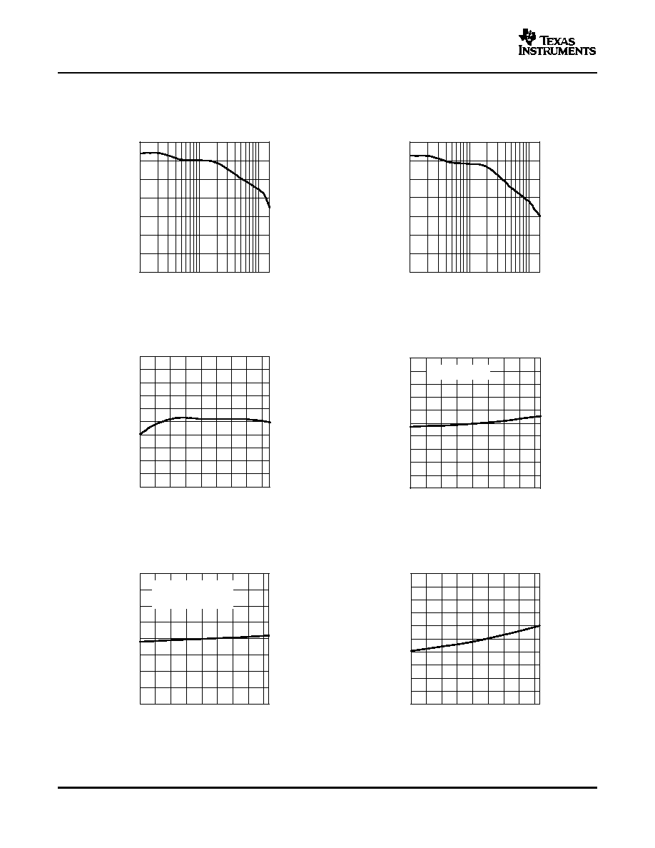
TYPICAL CHARACTERISTICS (continued)
SPURIOUS FREE DYNAMIC RANGE
TOTAL HARMONIC DISTORTION
vs
vs
INPUT FREQUENCY
INPUT FREQUENCY
Figure 16.
Figure 17.
INTERNAL REFERENCE VOLTAGE
BIPOLAR ZERO SCALE ERROR
vs
vs
FREE-AIR TEMPERATURE
FREE-AIR TEMPERATURE
Figure 18.
Figure 19.
FULL SCALE ERROR
SUPPLY CURRENT
vs
vs
FREE-AIR TEMPERATURE
FREE-AIR TEMPERATURE
Figure 20.
Figure 21.
14
www.ti.com
50
55
60
65
70
75
80
85
90
95
100
0
1
2
3
4
5
6
7
8
9
10 11
Performance
ESR - Resistance -
W
2.2
µ
F Capacitor on
CAP Pin (pin 6)
|THD|
SINAD
0
500
1000
1500
2000
2500
3000
3500
4000
4500
-3
-2
-1
0
1
2
3
4
149
2082
4224
4224
1484
238
11
Hits
Code
8192
Conversions
of a DC Input
-2.5
-2
-1.5
-1
-0.5
0
0.5
1
1.5
2
2.5
0
16384
32768
49152
65536
INL - LSBs
Code
f
s
= 250 KSPS
-2.5
-2
-1.5
-1
-0.5
0
0.5
1
1.5
2
2.5
0
16384
32768
49152
65536
DNL - LSBs
Code
f
s
= 250 KSPS
ADS8509
SLAS324A ≠ OCTOBER 2004 ≠ REVISED JUNE 2005
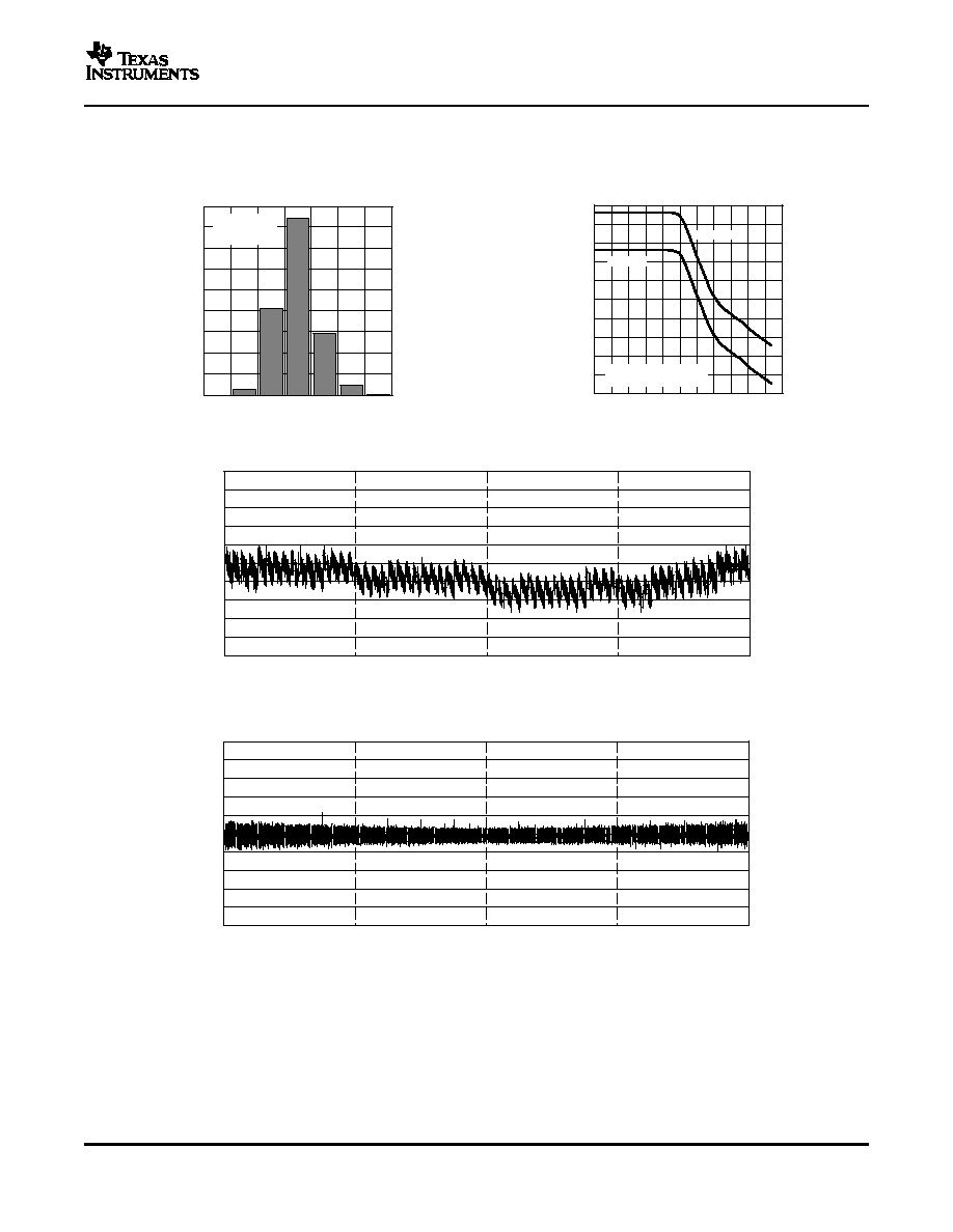
TYPICAL CHARACTERISTICS (continued)
HISTOGRAM
PERFORMANCE
vs
CAP PIN CAPACITOR ESR
Figure 22.
Figure 23.
INTEGRAL NONLINEARITY
Figure 24.
DIFFERENTIAL NONLINEARITY
Figure 25.
15
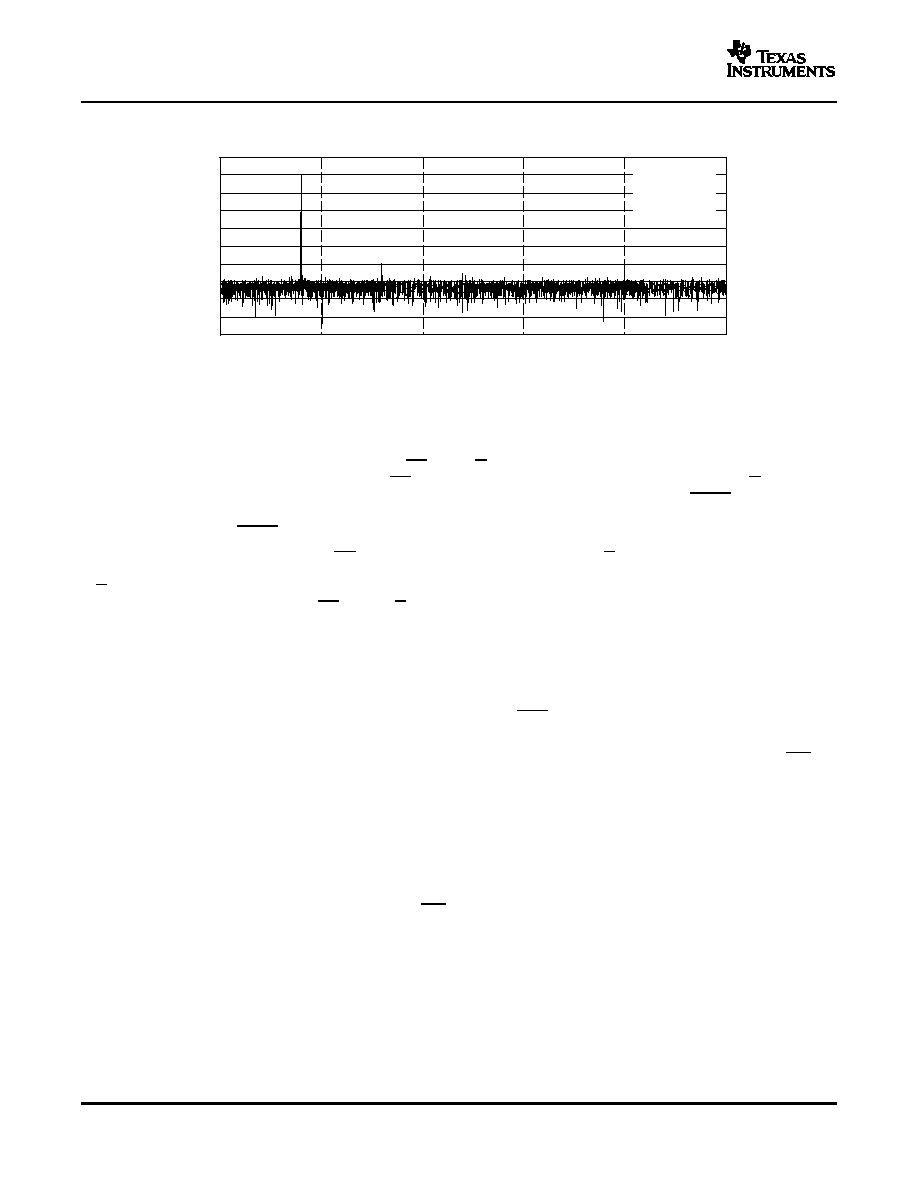
www.ti.com
-180
-160
-140
-120
-100
-80
-60
-40
-20
0
20
0
25
50
75
100
125
8192 Points,
f
s
= 250 KSPS,
f
i
= 20 kHz, 0 dB
SINAD = 86.0 dB,
THD = -98.7 dB
Amplitude - dB
f - Frequency - kHz
BASIC OPERATION
READING DATA
INTERNAL DATACLK
EXTERNAL DATACLK
ADS8509
SLAS324A ≠ OCTOBER 2004 ≠ REVISED JUNE 2005
TYPICAL CHARACTERISTICS (continued)
FFT (20 kHz Input)
Figure 26.
Two signals control conversion in the ADS8509: CS and R/C. These two signals are internally ORed together. To
start a conversion the chip must be selected, CS low, and the conversion signal must be active, R/C low. Either
signal can be brought low first. Conversion starts on the falling edge of the second signal. BUSY goes low when
conversion starts and returns high after the data from that conversion is shifted into the internal storage register.
Sampling begins when BUSY goes high.
To reduce the number of control pins CS can be tied low permanently. The R/C pin now controls conversion and
data reading exclusively. In the external clock mode this means that the ADS8509 will clock out data whenever
R/C is brought high and the external clock is active. In the internal clock mode data is clocked out every convert
cycle regardless of the states of CS and R/C. The ADS8509 provides a TAG input for cascading multiple
converters together.
The conversion result is available as soon as BUSY returns to high therefore, data always represents the
conversion previously completed even when it is read during a conversion. The ADS8509 outputs serial data in
either straight binary or binary two's compliment format. The SB/BTC pin controls the format. Data is shifted out
MSB first. The first conversion immediately following a power-up will not produce a valid conversion result.
Data can be clocked out with either the internally generated clock or with an external clock. The EXT/INT pin
controls this function. If external clock is used the TAG input can be used to daisy-chain multiple ADS8509 data
pins together.
In the internal clock mode data for the previous conversion is clocked out during each conversion period. The
internal data clock is synchronized to the internal conversion clock so that is does not interfere with the
conversion process.
The DATACLK pin becomes an output when EXT/INT is low. 16 clock pulses are generated at the beginning of
each conversion after timing t
8
is satisfied, i.e. you can only read previous conversion result during conversion.
DATACLK returns to low when it is inactive. The 16 bits of serial data are shifted out the DATA pin synchronous
to this clock with each bit available on a rising and then a falling edge. DATA pin returns to the state of TAG pin
input sensed at the start of transmission.
The external clock mode offers several ways to retrieve conversion results. However, since the external clock
cannot be synchronized to the internal conversion clock care must be taken to avoid corrupting the data.
16
www.ti.com
TAG FEATURE
ADS8509
SLAS324A ≠ OCTOBER 2004 ≠ REVISED JUNE 2005
When EXT/INT is set high, the R/C and CS signals control the read state. When the read state is initiated the
result from the previously completed conversion is shifted out the DATA pin synchronous to the external clock
that is connected to the DATACLK pin. Each bit is available on a falling and then a rising edge. The maximum
external clock speed of 28.5 MHz allows data shifted out quickly either at the beginning of conversion or the
beginning of sampling.
There are several modes of operation available when using an external clock. It is recommended that the
external clock run only while reading data. This is the discontinuous clock mode. Since the external clock is not
synchronized to the internal clock that controls conversion slight changes in the external clock can cause
conflicts that can corrupt the conversion process. Specifications with a continuously running external clock
cannot be guaranteed. It is especially important that the external clock does not run during the second half of the
conversion cycle (approximately the time period specified by t
d11
, see timing table).
In the discontinuous clock mode data can be read during conversion or during sampling, with or without a SYNC
pulse. Data read during a conversion must meet the t
d11
timing specification. Data read during sampling must be
complete before starting a conversion.
Whether reading during sampling or during conversion a SYNC pulse is generated whenever at least one rising
edge of the external clock occurs while the part is not in the read state. In the discontinuous external clock with
SYNC mode a SYNC pulse follows the first rising edge after the read command. The data is shifted out after the
SYNC pulse. The first rising clock edge after the read command generates a SYNC pulse. The SYNC pulse can
be detected on the next falling edge and then the next rising edge. Successively, each bit can be read first on the
falling edge and then on the next rising edge. Thus 17 clock pulses after the read command are required to read
on the falling edge. 18 clock pulses are necessary to read on the rising edge.
Table 2. DATACLK Pulses
DATACLK PULSES REQUIRED
DESCRIPTION
WITH SYNC
WITHOUT SYNC
Read on falling edge of DATACLK
17
16
Read on rising edge of DATACLK
18
17
If the clock is entirely inactive when not in the read state no SYNC pulse is generated. In this case the first rising
clock edge shifts out the MSB. The MSB can be read on the first falling edge or on the next rising edge. In this
discontinuous external clock mode with no SYNC, 16 clocks are necessary to read the data on the falling edge
and 17 clocks for reading on the rising edge. Data always represents the conversion already completed.
The TAG feature allows the data from multiple ADS8509 converters to be read on a single serial line. The
converters are cascaded together using the DATA pins as outputs and the TAG pins as inputs as illustrated in
Figure 27
. The DATA pin of the last converter drives the processor's serial data input. Data is then shifted
through each converter, synchronous to the externally supplied data clock, onto the serial data line. The internal
clock cannot be used for this configuration.
The preferred timing uses the discontinuous, external, data clock during the sampling period. Data must be read
during the sampling period because there is not sufficient time to read data from multiple converters during a
conversion period without violating the t
d11
constraint (see the EXTERNAL DATACLOCK section). The sampling
period must be sufficiently long to allow all data words to be read before starting a new conversion.
Note, in
Figure 27
, that a NULL bit separates the data word from each converter. The state of the DATA pin at
the end of a READ cycle reflects the state of the TAG pin at the start of the cycle. This is true in all READ
modes, including the internal clock mode. For example, when a single converter is used in the internal clock
mode the state of the TAG pin determines the state of the DATA pin after all 16 bits have shifted out. When
multiple converters are cascaded together this state forms the NULL bit that separates the words. Thus, with the
TAG pin of the first converter grounded as shown in
Figure 27
the NULL bit becomes a zero between each data
word.
17
www.ti.com
External
DATACLK
.
2
3
4
35
34
36
17
16
20
21
19
1
Null
D
Q
A00
D
Q
Null
D
Q
B00
D
Q
A15
D
Q
A16
D
Q
B15
D
Q
B16
D
Q
TAG(A)
TAG(B)
DATA (A)
DATA (B)
DATACLK
(both A & B )
SYNC
(both A & B )
(both A & B )
DATA ( B )
Nth Conversion Data
B15
A15
B00
B13
B14
B01
A00
A14
A13
A01
DATA ( A )
A15
A00
A13
A14
A01
18
Null
A
Null
B
Null
A
ADS8509A
TAG
DATA
DATACLK
ADS 8509B
TAG
DATA
DATACLK
Processor
SCLK
GPIO
GPIO
SDI
TAG(A) = 0
TAG(A) = 0
R/C
CS
R/C
CS
R/C
BUSY
EXT/INT tied high, CS of both converter A and B, TAG input of converter A are tied low.
ANALOG INPUTS
ADS8509
SLAS324A ≠ OCTOBER 2004 ≠ REVISED JUNE 2005
Figure 27. Timing of TAG Feature With Single Conversion (Using External DATACLK)
The ADS8509 has six analog input ranges as shown in
Table 3
. The offset and gain specifications are factory
calibrated with 0.1%, º-W, external resistors as shown in
Figure 29
and
Figure 30
. The external resistors can be
omitted if larger gain and offset errors are acceptable or if using software calibration. The hardware trim circuitry
shown in
Figure 29
and
Figure 30
can reduce the errors to zero.
The analog input pins R1
IN
, R2
IN
, and R3
IN
have ±25-V overvoltage protection. The input signal must be
referenced to AGND1. This will minimized the ground loop problem typical to analog designs. The analog input
should be driven by a low impedance source. A typical driving circuit using OPA627 or OPA132 is shown in
Figure 28
.
The ADS8509 can operate with its internal 2.5-V reference or an external reference. An external reference
connected to pin 6 (REF) bypasses the internal reference. The external reference must drive the 4-k
resistor
that separates pin 6 from the internal reference (see the illustration on page 1). The load will vary with the
difference between the internal and external reference voltages. The external reference voltage can vary from
2.3 V to 2.7 V. The internal reference will be approximately 2.5 V. The reference, whether internal or external, is
buffered internally with a buffer with its output on pin 5 (CAP).
The ADS8509 is factory tested with 2.2-µF capacitors connected to pins 5 and 6 (CAP and REF). Each capacitor
should be placed as close as possible to its pin. The capacitor on pin 6 band limits the internal reference noise. A
smaller capacitor can be used but it may degrade SNR and SINAD. The capacitor on pin 5 stabilizes the
reference buffer and provides switching charge to the CDAC during conversion. Capacitors smaller than 1 µF
can cause the buffer to become unstable may not hold sufficient charge for the CDAC. The parts are tested to
specifications with 2.2 µF so larger capacitors are not necessary. The equivalent series resistor (ESR) of these
compensation capacitors is also critical. Keep the total ESR under 3
. See the TYPICAL CHARACTERISTICS
section concerning how ESR affects performance.
Neither the internal reference nor the buffer should be used to drive an external load. Such loading can degrade
performance. Any load on the internal reference causes a voltage drop across the 4-k
resistor and will affect
gain. The internal buffer is capable of driving ±2-mA loads but any load can cause perturbations of the reference
at the CDAC, degrading performance. It should be pointed out that, unlike other competitor's parts with similar
input structure, the ADS8509 does not require a second high speed amplifier used as buffer to isolate the CAP
pin from the signal dependent current in the R3
IN
pin but can tolerate it if one do exist.
18
www.ti.com
OPA 627
GND
GND
GND
GND
GND
Pin 1
Pin 7
-
Pin 2
+
Pin3
Pin4
Pin 6
-15 V
+15 V
Vin
2.2
m
F
100 nF
2 k
W
22 pF
2 k
W
22 pF
200
W
100
W
33.2 k
W
2.2
m
F
2.2
m
F
100 nF
2.2
m
F
R1
IN
AGND1
R2
IN
R3
IN
CAP
REF
ADS8509
OPA 132
or
AGND2
DGND
GND
ADS8509
SLAS324A ≠ OCTOBER 2004 ≠ REVISED JUNE 2005
The external reference voltage can vary from 2.3 V to 2.7 V. The reference voltage determines the size of the
least significant bit (LSB). The larger reference voltages produce a larger LSB, which can improve SNR. Smaller
reference voltages can degrade SNR.
Figure 28. Typical Driving Circuitry (±10 V, No Trim)
19

www.ti.com
ADS8509
SLAS324A ≠ OCTOBER 2004 ≠ REVISED JUNE 2005
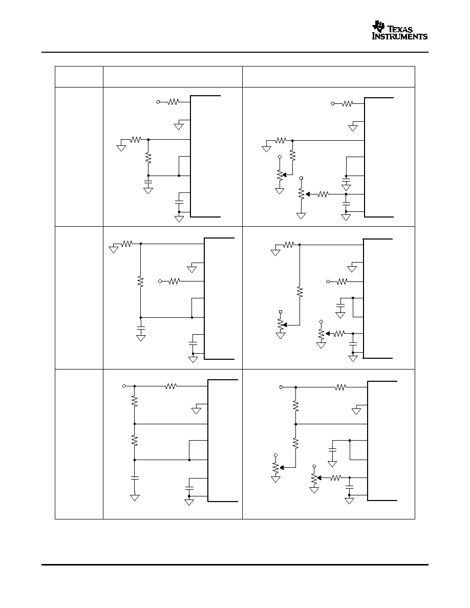
Table 3. Input Range Connections (see
Figure 29
and
Figure 30
for complete
information)
ANALOG
CONNECT R1
IN
VIA
CONNECT R2
IN
VIA
CONNECT
IMPEDANCE
INPUT RANGE
200
TO
100
TO
R3 TO
±10 V
V
IN
AGND
CAP
11.5 k
±5 V
AGND
V
IN
CAP
6.7 k
±3.33 V
V
IN
V
IN
CAP
5.4 k
0 V to 10 V
AGND
V
IN
AGND
6.7 k
0 V to 5 V
AGND
AGND
V
IN
5.0 k
0 V to 4 V
V
IN
AGND
V
IN
5.4 k
Table 4. Control Truth Table
SPECIFIC FUNCTION
CS
R/C
BUSY
EXT/INT
DATACLK
PWRD
SB/BTC
OPERATION
Initiate conversion and out-
1 > 0
0
1
0
Output
0
x
Initiates conversion n. Data from conversion n - 1
put data using internal clock
clocked out on DATA synchronized to 16 clock
0
1 > 0
1
0
Output
0
x
pulses output on DATACLK.
Initiate conversion and out-
1 > 0
0
1
1
Input
0
x
Initiates conversion n.
put data using external clock
0
1 > 0
1
1
Input
0
x
Initiates conversion n.
1 > 0
1
1
1
Input
x
x
Outputs data with or without SYNC pulse. See
section Reading Data.
1 > 0
1
0
1
Input
0
x
Outputs data with or without SYNC pulse. See
section Reading Data.
0
0 > 1
0
1
Input
0
x
No actions
0
0
0 > 1
x
x
0
x
This is an acceptable condition.
Power down
x
x
x
x
x
0
x
Analog circuitry powered. Conversion can pro-
ceed..
x
x
x
x
x
1
x
Analog circuitry disabled. Data from previous
conversion maintained in output registers.
Selecting output format
x
x
x
x
x
x
0
Serial data is output in binary 2s complement
format.
x
x
x
x
x
x
1
Serial data is output in straight binary format.
Table 5. Output Codes and Ideal Input Voltages
DIGITAL OUTPUT
BINARY 2's
STRAIGHT
DESCRIP-
ANALOG INPUT
COMPLEMENTS
BINARY
TION
(SB/BTC LOW)
(SB/BTC HIGH)
BINARY CODE
HEX CODE
BINARY CODE
HEX CODE
Full-scale
±10
±5
±3.33 V
0 V to 10 V
0 V to 5 V
0 V to 4 V
range
Least signifi-
cant bit
305 µV
153 µV
102 µV
153 µV
76 µV
61 µV
(LSB)
Full scale
9.999695 V
4.999847 V
3.333231 V
9.999847 V
4.999924 V
3.999939 V
0111 1111 1111 1111
7FFF
1111 1111 1111 1111
FFFF
(FS - 1LSB)
Midscale
0 V
0 V
0 V
5 V
2.5 V
2 V
0000 0000 0000 0000
0000
1000 0000 0000 0000
8000
One LSB
below
-305 µV
153 µV
±102 µV
4.999847 V
2.499924 V
1.999939 V
1111 1111 1111 1111
FFFF
0111 1111 1111 1111
7FFF
midscale
-Full scale
-10 V
-5 V
-3.333333 V
0 V
0 V
0 V
1000 0000 0000 0000
8000
0000 0000 0000 0000
0000
20
www.ti.com
+
+
+ 5 V
+
+
200
100
V
IN
33.2 k
2.2
µ
F
2.2
µ
F
R1
IN
AGND1
R2
IN
R3
IN
CAP
REF
AGND2
200
33.2 k
50 k
V
IN
100
R1
IN
AGND1
R2
IN
R3
IN
CAP
REF
AGND2
2.2
µ
F
+ 5 V
50 k
2.2
µ
F
576 k
+
+
+
+
R1
IN
AGND1
R2
IN
R3
IN
CAP
REF
AGND2
200
100
V
IN
2.2
µ
F
2.2
µ
F
33.2 k
200
33.2 k
+5 V
50 k
2.2
µ
F
100
V
IN
50 k
2.2
µ
F
576 k
R1
IN
AGND1
R2
IN
R3
IN
CAP
REF
AGND2
+
+
+
+
R1
IN
AGND1
R2
IN
R3
IN
CAP
REF
AGND2
V
IN
200
100
33.2 k
2.2
µ
F
2.2
µ
F
V
IN
200
100
33.2 k
+5 V
+5 V
+5 V
50 k
50 k
2.2
µ
F
576 k
2.2
µ
F
R1
IN
AGND1
R2
IN
R3
IN
CAP
REF
AGND2
Input Range
0 V - 10 V
0 V - 5 V
0 V - 4 V
Without Trim
With Trim
(Adjust Offset First at 0 V, Then Adjust Gain)
ADS8509
SLAS324A ≠ OCTOBER 2004 ≠ REVISED JUNE 2005
Figure 29. Offset/Gain Circuits for Unipolar Input Ranges
21
www.ti.com
Input Range
±
10 V
±
5 V
±
3.3 V
Without Trim
With Trim
(Adjust Offset First at 0 V, Then Adjust Gain)
+
+
+
+
R1
IN
AGND1
R2
IN
R3
IN
CAP
REF
AGND2
R1
IN
AGND1
R2
IN
R3
IN
CAP
REF
AGND2
200
100
V
IN
33.2 k
2.2
µ
F
2.2
µ
F
33.2 k
200
100
2.2
µ
F
+5 V
50 k
576 k
2.2
µ
F
50 k
+5 V
2.2 F
2.2 F
+
+
V
IN
200
V
IN
200
R1
IN
AGND1
R2
IN
R3
IN
CAP
REF
AGND2
R1
IN
AGND1
R2
IN
R3
IN
CAP
REF
AGND2
100
100
33.2 k
33.2 k
+5 V
+5 V
+
+
2.2
µ
F
2.2
µ
F
576 k
50 k
50 k
2.2 F
2.2 F
+
+
V
IN
R1
IN
AGND1
R2
IN
R3
IN
CAP
REF
AGND2
R1
IN
AGND1
R2
IN
R3
IN
CAP
REF
AGND2
V
IN
200
200
100
100
33.2 k
33.2 k
+
+
2.2
µ
F
2.2
µ
F
576 k
+5 V
50 k
50 k
+5 V
V
IN
ADS8509
SLAS324A ≠ OCTOBER 2004 ≠ REVISED JUNE 2005
Figure 30. Offset/Gain Circuits for Bipolar Input Ranges
22
PACKAGING INFORMATION
Orderable Device
Status
(1)
Package
Type
Package
Drawing
Pins Package
Qty
Eco Plan
(2)
Lead/Ball Finish
MSL Peak Temp
(3)
ADS8509IBDB
ACTIVE
SSOP
DB
28
50
TBD
Call TI
Call TI
ADS8509IBDBR
ACTIVE
SSOP
DB
28
2000
TBD
Call TI
Call TI
ADS8509IBDBRG4
ACTIVE
SSOP
DB
28
2000
TBD
Call TI
Call TI
ADS8509IBDW
ACTIVE
SOIC
DW
20
25
Green (RoHS &
no Sb/Br)
CU NIPDAU
Level-2-260C-1 YEAR
ADS8509IBDWR
ACTIVE
SOIC
DW
20
2000 Green (RoHS &
no Sb/Br)
CU NIPDAU
Level-2-260C-1 YEAR
ADS8509IBDWRG4
ACTIVE
SOIC
DW
20
2000 Green (RoHS &
no Sb/Br)
CU NIPDAU
Level-2-260C-1 YEAR
ADS8509IDB
ACTIVE
SSOP
DB
28
50
Green (RoHS &
no Sb/Br)
CU NIPDAU
Level-2-260C-1 YEAR
ADS8509IDBR
ACTIVE
SSOP
DB
28
2000 Green (RoHS &
no Sb/Br)
CU NIPDAU
Level-2-260C-1 YEAR
ADS8509IDBRG4
ACTIVE
SSOP
DB
28
2000 Green (RoHS &
no Sb/Br)
CU NIPDAU
Level-2-260C-1 YEAR
ADS8509IDW
ACTIVE
SOIC
DW
20
25
Green (RoHS &
no Sb/Br)
CU NIPDAU
Level-2-260C-1 YEAR
ADS8509IDWR
ACTIVE
SOIC
DW
20
2000 Green (RoHS &
no Sb/Br)
CU NIPDAU
Level-2-260C-1 YEAR
ADS8509IDWRG4
ACTIVE
SOIC
DW
20
2000 Green (RoHS &
no Sb/Br)
CU NIPDAU
Level-2-260C-1 YEAR
(1)
The marketing status values are defined as follows:
ACTIVE: Product device recommended for new designs.
LIFEBUY: TI has announced that the device will be discontinued, and a lifetime-buy period is in effect.
NRND: Not recommended for new designs. Device is in production to support existing customers, but TI does not recommend using this part in
a new design.
PREVIEW: Device has been announced but is not in production. Samples may or may not be available.
OBSOLETE: TI has discontinued the production of the device.
(2)
Eco
Plan
-
The
planned
eco-friendly
classification:
Pb-Free
(RoHS)
or
Green
(RoHS
&
no
Sb/Br)
-
please
check
http://www.ti.com/productcontent
for the latest availability information and additional product content details.
TBD: The Pb-Free/Green conversion plan has not been defined.
Pb-Free (RoHS): TI's terms "Lead-Free" or "Pb-Free" mean semiconductor products that are compatible with the current RoHS requirements
for all 6 substances, including the requirement that lead not exceed 0.1% by weight in homogeneous materials. Where designed to be soldered
at high temperatures, TI Pb-Free products are suitable for use in specified lead-free processes.
Green (RoHS & no Sb/Br): TI defines "Green" to mean Pb-Free (RoHS compatible), and free of Bromine (Br) and Antimony (Sb) based flame
retardants (Br or Sb do not exceed 0.1% by weight in homogeneous material)
(3)
MSL, Peak Temp. -- The Moisture Sensitivity Level rating according to the JEDEC industry standard classifications, and peak solder
temperature.
Important Information and Disclaimer:The information provided on this page represents TI's knowledge and belief as of the date that it is
provided. TI bases its knowledge and belief on information provided by third parties, and makes no representation or warranty as to the
accuracy of such information. Efforts are underway to better integrate information from third parties. TI has taken and continues to take
reasonable steps to provide representative and accurate information but may not have conducted destructive testing or chemical analysis on
incoming materials and chemicals. TI and TI suppliers consider certain information to be proprietary, and thus CAS numbers and other limited
information may not be available for release.
In no event shall TI's liability arising out of such information exceed the total purchase price of the TI part(s) at issue in this document sold by TI
to Customer on an annual basis.
PACKAGE OPTION ADDENDUM
www.ti.com
3-Oct-2005
Addendum-Page 1
MECHANICAL DATA
MSSO002E ≠ JANUARY 1995 ≠ REVISED DECEMBER 2001
POST OFFICE BOX 655303
∑
DALLAS, TEXAS 75265
DB (R-PDSO-G**)
PLASTIC SMALL-OUTLINE
4040065 /E 12/01
28 PINS SHOWN
Gage Plane
8,20
7,40
0,55
0,95
0,25
38
12,90
12,30
28
10,50
24
8,50
Seating Plane
9,90
7,90
30
10,50
9,90
0,38
5,60
5,00
15
0,22
14
A
28
1
20
16
6,50
6,50
14
0,05 MIN
5,90
5,90
DIM
A MAX
A MIN
PINS **
2,00 MAX
6,90
7,50
0,65
M
0,15
0
∞
≠ 8
∞
0,10
0,09
0,25
NOTES: A. All linear dimensions are in millimeters.
B. This drawing is subject to change without notice.
C. Body dimensions do not include mold flash or protrusion not to exceed 0,15.
D. Falls within JEDEC MO-150

IMPORTANT NOTICE
Texas Instruments Incorporated and its subsidiaries (TI) reserve the right to make corrections, modifications,
enhancements, improvements, and other changes to its products and services at any time and to discontinue
any product or service without notice. Customers should obtain the latest relevant information before placing
orders and should verify that such information is current and complete. All products are sold subject to TI's terms
and conditions of sale supplied at the time of order acknowledgment.
TI warrants performance of its hardware products to the specifications applicable at the time of sale in
accordance with TI's standard warranty. Testing and other quality control techniques are used to the extent TI
deems necessary to support this warranty. Except where mandated by government requirements, testing of all
parameters of each product is not necessarily performed.
TI assumes no liability for applications assistance or customer product design. Customers are responsible for
their products and applications using TI components. To minimize the risks associated with customer products
and applications, customers should provide adequate design and operating safeguards.
TI does not warrant or represent that any license, either express or implied, is granted under any TI patent right,
copyright, mask work right, or other TI intellectual property right relating to any combination, machine, or process
in which TI products or services are used. Information published by TI regarding third-party products or services
does not constitute a license from TI to use such products or services or a warranty or endorsement thereof.
Use of such information may require a license from a third party under the patents or other intellectual property
of the third party, or a license from TI under the patents or other intellectual property of TI.
Reproduction of information in TI data books or data sheets is permissible only if reproduction is without
alteration and is accompanied by all associated warranties, conditions, limitations, and notices. Reproduction
of this information with alteration is an unfair and deceptive business practice. TI is not responsible or liable for
such altered documentation.
Resale of TI products or services with statements different from or beyond the parameters stated by TI for that
product or service voids all express and any implied warranties for the associated TI product or service and
is an unfair and deceptive business practice. TI is not responsible or liable for any such statements.
Following are URLs where you can obtain information on other Texas Instruments products and application
solutions:
Products
Applications
Amplifiers
amplifier.ti.com
Audio
www.ti.com/audio
Data Converters
dataconverter.ti.com
Automotive
www.ti.com/automotive
DSP
dsp.ti.com
Broadband
www.ti.com/broadband
Interface
interface.ti.com
Digital Control
www.ti.com/digitalcontrol
Logic
logic.ti.com
Military
www.ti.com/military
Power Mgmt
power.ti.com
Optical Networking
www.ti.com/opticalnetwork
Microcontrollers
microcontroller.ti.com
Security
www.ti.com/security
Telephony
www.ti.com/telephony
Video & Imaging
www.ti.com/video
Wireless
www.ti.com/wireless
Mailing Address:
Texas Instruments
Post Office Box 655303 Dallas, Texas 75265
Copyright
2005, Texas Instruments Incorporated