 | –≠–ª–µ–∫—Ç—Ä–æ–Ω–Ω—ã–π –∫–æ–º–ø–æ–Ω–µ–Ω—Ç: ADS852Y | –°–∫–∞—á–∞—Ç—å:  PDF PDF  ZIP ZIP |

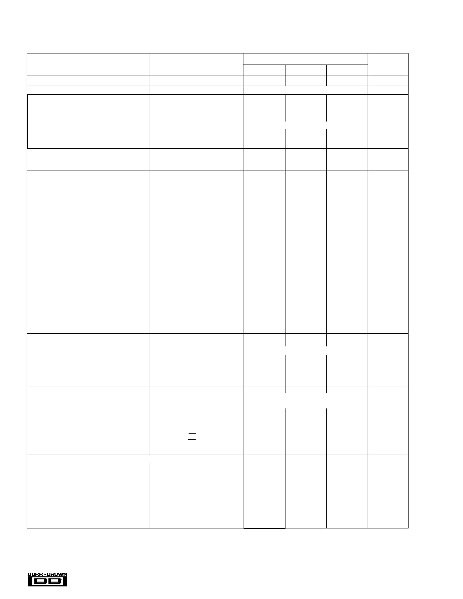
14-Bit
Pipelined
A/D Core
Reference and
Mode Select
Reference Ladder
and Driver
Timing Circuitry
Error
Correction
Logic
3-State
Outputs
T/H
D0
D13
∑
∑
∑
+V
S
ADS852
CLK
CLK
OE
SEL2
REFB
V
REF
REFT
VDRV
IN
2Vp-p
2Vp-p
CM
(+2.5V)
SEL1
OVR
IN
International Airport Industrial Park ∑ Mailing Address: PO Box 11400, Tucson, AZ 85734 ∑ Street Address: 6730 S. Tucson Blvd., Tucson, AZ 85706 ∑ Tel: (520) 746-1111 ∑ Twx: 910-952-1111
Internet: http://www.burr-brown.com/ ∑ FAXLine: (800) 548-6133 (US/Canada Only) ∑ Cable: BBRCORP ∑ Telex: 066-6491 ∑ FAX: (520) 889-1510 ∑ Immediate Product Info: (800) 548-6132
©
1998 Burr-Brown Corporation
PDS-1442
Printed in U.S.A. June, 1998
ADS852
Æ
14-Bit, 65MHz Sampling
ANALOG-TO-DIGITAL CONVERTER
TM
FEATURES
q
HIGH DYNAMIC RANGE:
High SFDR: 100dB at 20MHz f
IN
High SNR: 75dB at 20MHz f
IN
q
PREMIUM TRACK/HOLD:
High Bandwidth: 1GHz
Low Jitter: 0.25pS rms
Differential or Single-Ended Inputs
Selectable Full-Scale Input Range
q
FLEXIBLE CLOCKING:
Differential or Single-Ended
Accepts Sine or Square Wave Clocking
Down to 0.5Vp-p
Variable Threshold Level
DESCRIPTION
The ADS852 is a high-dynamic range 14-bit, 65MHz
pipelined analog-to-digital converter. It includes a high-
bandwidth linear track/hold that gives excellent spurious
performance up to and beyond the Nyquist rate. This high-
bandwidth track/hold also has a low jitter of only 0.25pS
rms, leading to excellent SNR performance. The clock input
can accept a low level differential sine wave or square wave
signal down to 0.5Vp-p, further improving the SNR perfor-
mance. It also accepts a single-ended clock signal and has
flexible threshold levels.
The ADS852 has a 4Vp-p differential input range (2Vp-p x
2 inputs, +16dBm) for optimum signal-to-noise ratio. The
differential operation gives the lowest even-order harmonic
components. A lower input voltage of 3Vp-p or 2Vp-p can
also be selected using the internal references, further opti-
mizing SFDR. Alternatively, a single-ended input range can
be used by tying the IN input to the common-mode voltage
if desired.
The ADS852 also provides an over-range flag that indicates
when the input signal has exceeded the converter's full-scale
range. This flag can also be used to reduce the gain of the
front end signal conditioning circuitry. It also employs
digital error correction techniques to provide excellent dif-
ferential linearity for demanding imaging applications. The
ADS852 is available in a small 48-lead TQFP package.
PRELIMINARY INFORMATION
SUBJECT TO CHANGE
WITHOUT NOTICE
APPLICATIONS
q
BASESTATION WIDEBAND RADIOS:
CDMA, GSM, TDMA, 3G, AMPS, NMT
q
TEST INSTRUMENTATION
q
CCD IMAGING
2
Æ
ADS852
SPECIFICATIONS
At T
A
= full specified temperature range, differential input range = 1.5V to 3.5V, sampling rate = 65MHz, and external reference, unless otherwise noted.
+3V/+5V Logic Compatible CMOS
Straight Offset Binary
+3V/+5V Logic Compatible CMOS
ADS852Y
PARAMETER
CONDITIONS
MIN
TYP
MAX
UNITS
RESOLUTION
14 Guaranteed
Bits
SPECIFIED TEMPERATURE RANGE
Ambient Air
≠40 to +85
∞
C
ANALOG INPUT
Standard Differential Input Range
(2Vp-p x 2, +16dBm)
1.5
3.5
V
Optional Single-Ended Input Range
4Vp-p
0.5
4.5
V
Common-Mode Voltage
2.5
V
Optional Input Ranges
Selectable
2Vp-p (+10dBm) or 3Vp-p (+13dBm)
V
Analog Input Bias Current
1
µ
A
Track-Mode Input Bandwidth
≠3dBFS
1
GHz
Input Impedance
1.25 || 9
M
|| pF
CONVERSION CHARACTERISTICS
Sample Rate
1M
65M
Samples/s
Data Latency
7
Clk Cyc
DYNAMIC CHARACTERISTICS
Differential Linearity Error (largest code error)
f = 2.2MHz
±
0.5
±
1.0
LSB
f = 20MHz
±
0.5
LSB
No Missing Codes
Guaranteed
Integral Nonlinearity Error, f = 1MHz
±
0.5
±
2.0
LSBs
Spurious Free Dynamic Range
(1)
f = 2.2MHz
105
dBFS
(2)
f = 20MHz
100
dBFS
f = 31MHz
100
dBFS
Two-Tone Intermodulation Distortion
(3)
f = 4.5MHz and 5.5MHz (≠7dB each tone)
≠95
dBc
Signal-to-Noise Ratio (SNR)
f = 2.2MHz
75
dBFS
f = 20MHz
75
dBFS
f = 31MHz
75
dBFS
Signal-to-(Noise + Distortion) (SINAD)
f = 2.2MHz
75
dB
f = 20MHz
75
dB
f = 31MHz
74
dBFS
Output Noise
Input Grounded
TBD
LSBs rms
Aperture Delay Time
3
ns
Aperture Jitter
0.25
ps rms
Overvoltage Recovery Time
2
ns
Full-Scale Step Acquisition Time
5
ns
DIGITAL INPUTS
Convert Command (Start Conversion)
Rising Edge of Convert Clock
+0.5
+V
S
Vp-p
Logic Family (Other Clock Inputs)
High Level Input Current
(4)
(V
IN
= 5V)
100
µ
A
Low Level Input Current (V
IN
= 0V)
10
µ
A
High Level Input Voltage
+2.0
V
Low Level Input Voltage
+1.0
V
Input Capacitance
5
pF
DIGITAL OUTPUTS
Logic Family
Logic Coding
Low Output Voltage (I
OL
= 50
µ
A to 1.6mA)
VDRV = 3V
+0.2
V
High Output Voltage, (I
OH
= 50
µ
A to 0.5mA)
+2.5
V
Low Output Voltage, (I
OL
= 50
µ
A to 1.6mA)
VDRV = 5V
+0.2
V
High Output Voltage, (I
OH
= 50
µ
A to 1.6mA)
+2.5
V
3-State Enable Time
OE = L
20
40
ns
3-State Disable Time
OE = H
2
10
ns
Output Capacitance
5
pF
ACCURACY (Internal Reference, = 2V, Unless Otherwise Noted)
Zero Error (Referred to ≠FS)
at 25
∞
C
0.5
3.0
%FS
Zero Error Drift (Referred to ≠FS)
12
ppm/
∞
C
Gain Error
(5)
at 25
∞
C
±
1.5
±
2.5
%FS
Gain Error Drift
(5)
38
ppm/
∞
C
Gain Error
(6)
at 25
∞
C
±
0.75
±
1.5
%FS
Gain Error Drift
(6)
20
ppm/
∞
C
Power Supply Rejection of Gain
V
S
=
±
5%
68
dB
Internal REF Tolerance
Deviation from Ideal
±
10
±
50
mV
External REF Voltage Range
0.9
2
2.025
V
Reference Input Resistance
1.0
k

3
Æ
ADS852
POWER SUPPLY REQUIREMENTS
Supply Voltage: +V
S
Operating
+4.75
+5.0
+5.25
V
Supply Current: +I
S
Operating
120
mA
Output Driver Supply Current (VDRV)
12
mA
Power Dissipation: VDRV = 5V
670
740
mW
VDRV = 3V
650
720
mW
Power Down
Operating
20
mW
Thermal Resistance,
JA
48-Lead TQFP
∞
C/W
NOTES: (1) Spurious Free Dynamic Range refers to the magnitude of the largest harmonic. (2) dBFS means dB relative to Full Scale. (3) Two-tone
intermodulation distortion is referred to the largest fundamental tone. This number will be 6dB higher if it is referred to the magnitude of the two-tone fundamental
envelope. (4) A 50k
pull-down resistor is inserted internally. (5) Includes internal reference. (6) Excludes internal reference.
SPECIFICATIONS
(CONT)
At T
A
= full specified temperature range, differential input range = 1.5V to 3.5V, sampling rate = 65MHz, and external reference, unless otherwise noted.
ADS852Y
PARAMETER
CONDITIONS
MIN
TYP
MAX
UNITS
+V
S
....................................................................................................... +6V
Analog Input ........................................................... (≠0.3V) to (+V
S
+0.3V)
Logic Input ............................................................. (≠0.3V) to (+V
S
+0.3V)
Case Temperature ......................................................................... +100
∞
C
Junction Temperature .................................................................... +150
∞
C
Storage Temperature ..................................................................... +150
∞
C
PACKAGE
DRAWING
TEMPERATURE
PRODUCT
PACKAGE
NUMBER
(1)
RANGE
ADS852Y
48-Lead TQFP
xxx
≠40
∞
C to +85
∞
C
NOTE: (1) For detailed drawing and dimension table, please see end of data
sheet, or Appendix C of Burr-Brown IC Data Book.
ABSOLUTE MAXIMUM RATINGS
PACKAGE/ORDERING INFORMATION
ELECTROSTATIC
DISCHARGE SENSITIVITY
This integrated circuit can be damaged by ESD. Burr-Brown
recommends that all integrated circuits be handled with
appropriate precautions. Failure to observe proper handling
and installation procedures can cause damage.
ESD damage can range from subtle performance degradation
to complete device failure. Precision integrated circuits may
be more susceptible to damage because very small parametric
changes could cause the device not to meet its published
specifications.
The information provided herein is believed to be reliable; however, BURR-BROWN assumes no responsibility for inaccuracies or omissions. BURR-BROWN
assumes no responsibility for the use of this information, and all use of such information shall be entirely at the user's own risk. Prices and specifications are subject
to change without notice. No patent rights or licenses to any of the circuits described herein are implied or granted to any third party. BURR-BROWN does not
authorize or warrant any BURR-BROWN product for use in life support devices and/or systems.

4
Æ
ADS852
1
BYP
Bypass Point
2
+V
S
Supply Voltage
3
+V
S
Supply Voltage
4
+V
S
Supply Voltage
5
GND
Ground
6
I
CLK
Clock Input
7
I
CLK
Complementary Clock Input
8
GND
Ground
9
GND
Ground
10
O
OVR
Overrange Indicator
11
O
DV
Data Valid Pulse: HI = Data Vaild
12
O
D13
Most Significant Bit (MSB)
13
O
D12
Data Bit 12
14
O
D11
Data Bit 11
15
O
D10
Data Bit 10
16
O
D9
Data Bit 9
17
O
D8
Data Bit 8
18
O
D7
Data Bit 7
19
O
D6
Data Bit 6
20
O
D5
Data Bit 5
21
O
D4
Data Bit 4
22
O
D3
Data Bit 3
23
O
D2
Data Bit 2
24
O
D1
Data Bit 1
25
O
D0
Least Significant Bit (LSB)
26
VDRV
Output Bit Driver Voltage Supply
27
GND
Ground
28
OE
Output Enable: HI = High Impedance;
LO or Floating: Normal Operation
29
I
PD
Power Down: HI = Power Down; LO = Normal
30
I
BTC
HI = Binary Two's Complement;
LO = Straight Binary
31
GND
Ground
32
SEL2
Reference Select 2: See Table
33
SEL1
Reference Select 1: See Table
34
V
REF
Internal Reference Voltage
35
GND
Ground
36
GND
Ground
37
GND
Ground
38
GND
Ground
39
REFN
Bottom Reference Voltage Bypass
40
CM
Common-Mode Voltage (mid-scale)
41
REFP
Top Reference Voltage Bypass
42
GND
Ground
43
GND
Ground
44
I
IN
Complementary Analog Input
45
GND
Ground
46
I
IN
Analog Input
47
+V
S
Supply Voltage
48
+V
S
Supply Voltage
36
35
34
33
32
31
30
29
28
27
26
25
GND
GND
V
REF
SEL1
SEL2
GND
BTC
PD
OE
GND
VDRV
D0 (LSB)
+V
S
+V
S
IN
GND
IN
GND
GND
REFP
CM
REFN
GND
GND
D12
D11
D10
D9
D8
D7
D6
D5
D4
D3
D2
D1
1
2
3
4
5
6
7
8
9
10
11
12
BYP
+V
S
+V
S
+V
S
GND
CLK
CLK
GND
GND
OVR
DV
D13 (MSB)
48
47
46
45
44
43
42
41
40
39
38
13
14
15
16
17
18
19
20
21
22
23
37
24
ADS852Y
PIN
I/O
DESIGNATOR
DESCRIPTION
PIN
I/O
DESIGNATOR
DESCRIPTION
PIN DESCRIPTIONS
PIN DIAGRAM

5
Æ
ADS852
7 Clock Cycles
Data Invalid
t
D
t
L
t
H
t
CONV
N≠7
N≠6
N≠5
N≠4
N≠3
N≠2
N≠1
N
Data Out
Clock
Analog In
N
t
2
N+1
N+2
N+3
N+4
N+5
N+6
N+7
t
1
TIMING DIAGRAM
SYMBOL
DESCRIPTION
MIN
TYP
MAX
UNITS
t
CONV
Convert Clock Period
15.4
1
µ
s
ns
t
L
Clock Pulse Low
7.6
t
CONV
/2
ns
t
H
Clock Pulse High
7.6
t
CONV
/2
ns
t
D
Aperture Delay
3
ns
t
1
Data Hold Time, C
L
= 0pF
3.9
ns
t
2
New Data Delay Time, C
L
= 15pF max
12
ns
DESIRED
INTERNAL
FULL SCALE RANGE
SEL1
SEL2
V
REF
4Vp-p (2Vp-p x 2, +16dBm)
GND
GND
2V
3Vp-p (1.5Vp-p x 2, +13dBm)
GND
+V
S
1.5V
2Vp-p (1Vp-p x 2, +10dBm)
V
REF
GND
1V
TABLE, REFERENCE/FULL SCALE RANGE SELECT
For External Reference Operation, tie V
REF
to +V
S
, the full scale range will be 2X the reference value. For instance, selecting a 2V External Reference will set
the full scale values of 1.5V to 3.5V for both IN and IN inputs.