 | –≠–ª–µ–∫—Ç—Ä–æ–Ω–Ω—ã–π –∫–æ–º–ø–æ–Ω–µ–Ω—Ç: ADS931 | –°–∫–∞—á–∞—Ç—å:  PDF PDF  ZIP ZIP |
1
Æ
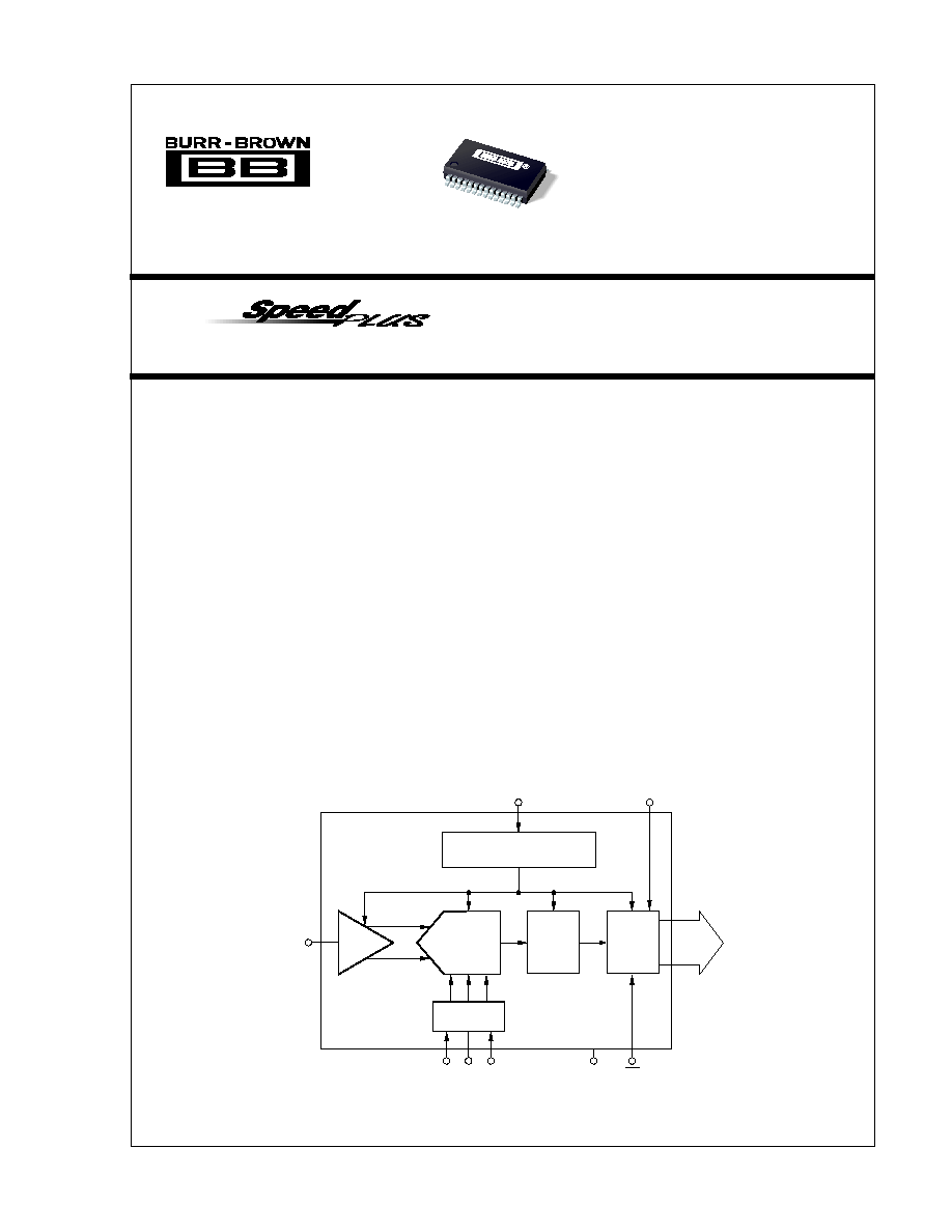
ADS931
Pipeline
A/D
Reference
Ladder
Timing
Circuitry
Error
Correction
Logic
3-State
Outputs
T/H
8-Bit
Digital
Data
CLK
ADS931
LV
DD
OE
Pwrdn
REFB
CM
REFT
IN
ADS931
Æ
FEATURES
q
+2.7V TO +5.5V SUPPLY OPERATION
q
LOW POWER: 69mW at +3V
q
ADJUSTABLE FULL SCALE RANGE WITH
EXTERNAL REFERENCE
q
NO MISSING CODES
q
POWER DOWN
q
28-LEAD SSOP PACKAGE
DESCRIPTION
The ADS931 is a high speed pipelined analog-to-
digital converter that is specified to operate from
standard +5V or +3V power supplies. This converter
includes a high bandwidth track/hold and an 8-bit
quantizer. The performance is specified with a single-
ended input range of 1V to 2V when operating off of
a +3V supply. This device also allows for standard
input ranges such as 2V to 4V or 2V to 3V, when
operating on +5V supplies. The full scale input range
is set by an external reference.
The ADS931 employs digital error correction tech-
niques to provide excellent differential linearity for
demanding imaging applications. Its low distortion and
high SNR give the extra margin needed for telecom-
munications, video and test instrumentation applica-
tions. This high performance A/D converter is speci-
fied for performance at a 30MHz sampling rate. The
ADS931 is available in a 28-Lead SSOP package.
8-Bit, 30MHz Sampling
ANALOG-TO-DIGITAL CONVERTER
TM
APPLICATIONS
q
BATTERY POWERED EQUIPMENT
q
CAMCORDERS
q
PORTABLE TEST EQUIPMENT
q
DIGITAL CAMERAS
q
COMMUNICATIONS
International Airport Industrial Park ∑ Mailing Address: PO Box 11400, Tucson, AZ 85734 ∑ Street Address: 6730 S. Tucson Blvd., Tucson, AZ 85706 ∑ Tel: (520) 746-1111 ∑ Twx: 910-952-1111
Internet: http://www.burr-brown.com/ ∑ FAXLine: (800) 548-6133 (US/Canada Only) ∑ Cable: BBRCORP ∑ Telex: 066-6491 ∑ FAX: (520) 889-1510 ∑ Immediate Product Info: (800) 548-6132
ADS931E
©
1996 Burr-Brown Corporation
PDS-1349C
Printed in U.S.A. March, 1998
2
Æ
ADS931
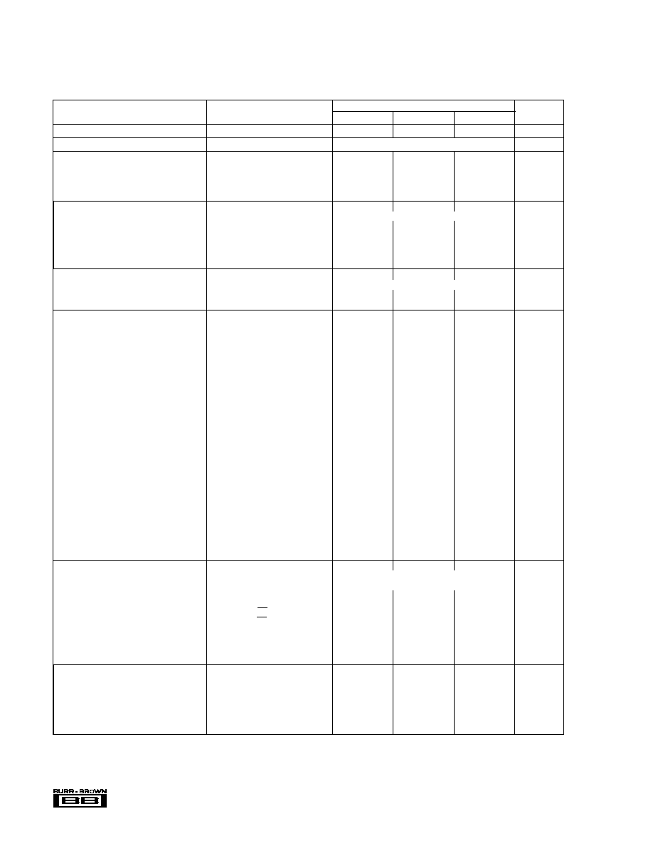
SPECIFICATIONS
At T
A
= full specified temperature range unless otherwise noted. +V
S
= LV
DD
= +3V, specified single-ended input (1V to 2V) and sampling rate = 30MHz, unless
otherwise specified. The input range is 2.25V to 3.25V when specified for +5V operation.
ADS931E
PARAMETER
CONDITIONS
MIN
TYP
MAX
UNITS
RESOLUTION
8
Bits
SPECIFIED TEMPERATURE RANGE
Ambient Air
≠40 to +85
∞
C
ANALOG INPUT
Specified Full Scale Input Range
(1)
1Vp-p
+1.0
+2.0
V
Common-mode Voltage
+1.5
V
Analog Input Bias Current
1
µ
A
Input Impedance
1.25 || 5
M
|| pF
DIGITAL INPUTS
Logic Family
TTL/HCT Compatible CMOS
High Input Voltage, V
IH
+2.0
LV
DD
V
Low Input Voltage, V
IL
+0.8
V
High Input Current, I
IH
±
10
µ
A
Low Input Current, I
IL
±
10
µ
A
Input Capacitance
5
pF
CONVERSION CHARACTERISTICS
Start Conversion
Rising Edge of Convert Clock
Sample Rate
10k
30M
Samples/s
Data Latency
5
Clk Cycles
DYNAMIC CHARACTERISTICS
Differential Linearity Error
V
S
= +3V and +5V
f = 500MHz
±
0.7
±
1.0
LSB
f = 12.5MHz
±
0.7
LSB
No Missing Codes
V
S
= +3V and +5V
Guaranteed
Integral Nonlinearity Error, f = 500kHz
V
S
= +3V and +5V
±
1.0
±
2.5
LSB
Spurious Free Dynamic Range
(2)
V
S
= +3V and +5V
f = 500kHz (≠1dBFS input)
49
dBFS
(3)
f = 12.5MHz (≠1dBFS input)
43
49
dBFS
Two-Tone Intermodulation Distortion
(4)
f = 3.6MHz and 3.5MHz (≠7dBFS each tone)
54
dBFS
Signal-to-Noise Ratio (SNR)
V
S
= +3V and +5V
f = 500kHz (≠1dBFS input)
48
dB
f = 12.5MHz (≠1dBFS input)
44
48
dB
Signal-to-(Noise + Distortion) (SINAD)
V
S
= +3V and +5V
f = 500kHz (≠1dBFS input)
45
dB
f = 12.5MHz (≠1dBFS input)
40
45
dB
Effective Number of Bits
f = 12MHz
(5)
7.2
Bits
Differential Gain Error
NTSC, PAL
2.3
%
Differential Phase Error
NTSC, PAL
1
degrees
Output Noise
Input AC-Grounded
0.2
LSBs rms
Aperture Delay Time
2
ns
Aperture Jitter
7
ps rms
Analog Input Bandwidth
Small Signal
≠20dBFS Input
350
MHz
Full Power
0dBFS Input
100
MHz
Overvoltage Recovery Time
(6)
2
ns
DIGITAL OUTPUTS
C
L
= 15pF
Logic Family
TTL/HCT Compatible CMOS
Logic Coding
Straight Offset Binary
High Output Voltage, V
OH
2.4
V
DD
V
Low Output Voltage, V
OL
0.4
V
3-State Enable Time
OE = L
20
40
ns
3-State Disable Time
OE = H
2
10
ns
Internal Pull-Down
50
k
Power-Down Enable Time
Pwrdn = L
133
ns
Power-Down Disable Time
Pwrdn = H
18
ns
Internal Pull-Down
50
k
ACCURACY
V
S
= +3V and +5V
Gain Error
2.4
3.5
%FS
Input Offset
(7)
Referred to Ideal Midscale
±
6.5
±
25
mV
Power Supply Rejection (Gain)
V
S
= +10%
42
75
dB
External REFT Voltage Range
REFB +0.5
2
V
S
≠0.8
V
External REFB Voltage Range
0.8
1
REFT ≠0.5
V
Reference Input Resistance
4
k
3
Æ
ADS931
The information provided herein is believed to be reliable; however, BURR-BROWN assumes no responsibility for inaccuracies or omissions. BURR-BROWN
assumes no responsibility for the use of this information, and all use of such information shall be entirely at the user's own risk. Prices and specifications are subject
to change without notice. No patent rights or licenses to any of the circuits described herein are implied or granted to any third party. BURR-BROWN does not
authorize or warrant any BURR-BROWN product for use in life support devices and/or systems.
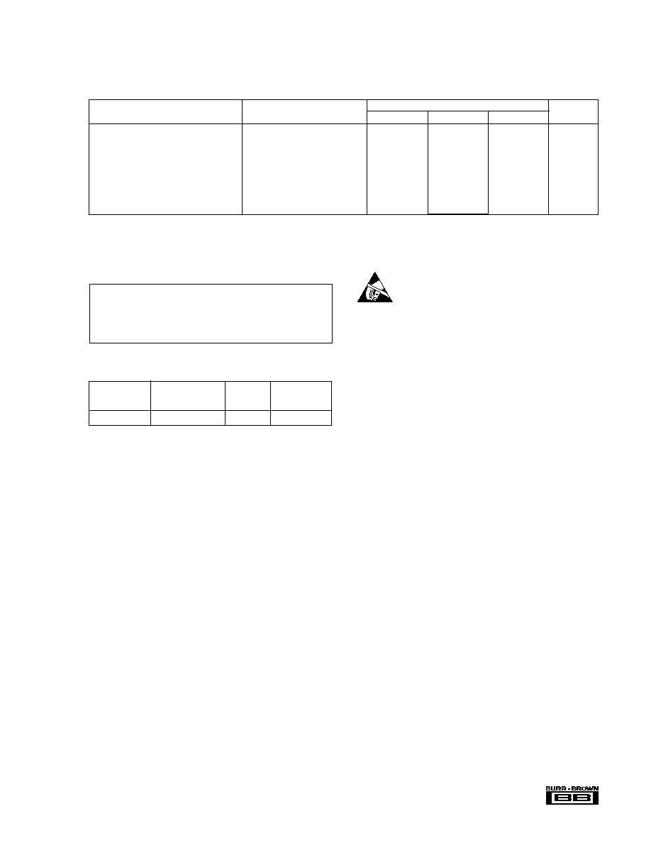
SPECIFICATIONS
(CONT)
At T
A
= full specified temperature range unless otherwise noted. +V
S
= LV
DD
= +3V, specified single-ended input (1V to 2V) and sampling rate = 30MHz, unless
otherwise specified. The input range is 2.25V to 3.25V when specified for +5V operation.
POWER SUPPLY REQUIREMENTS
Supply Voltage: +V
S
Operating
+2.7
+3.0
+5.5
V
Supply Current: +I
S
V
S
= +3V
23
29
mA
Power Dissipation
V
S
= +3V
69
87
mW
V
S
= +5V
154
mW
Power Dissipation (Power Down)
V
S
= +3V
10
mW
V
S
= +5V
15
mW
Thermal Resistance,
JA
28-Lead SSOP
50
∞
C/W
ADS931E
PARAMETER
CONDITIONS
MIN
TYP
MAX
UNITS
NOTES: (1) The single-ended input range is set by REFB and REFT values. (2) Spurious Free Dynamic Range refers to the magnitude of the largest harmonic.
(3) dBFS is dB relative to full scale. (4) Two-tone intermodulation distortion is referred to as the largest fundamental tone. (5) Based on (SINAD ≠1.76) /6.02. (6) No
"Rollover" of bits. (7) Offset deviation from ideal negative full scale.
ELECTROSTATIC
DISCHARGE SENSITIVITY
This integrated circuit can be damaged by ESD. Burr-Brown
recommends that all integrated circuits be handled with
appropriate precautions. Failure to observe proper handling
and installation procedures can cause damage.
ESD damage can range from subtle performance degradation
to complete device failure. Precision integrated circuits may
be more susceptible to damage because very small parametric
changes could cause the device not to meet its published
specifications.
+V
S
....................................................................................................... +6V
Analog Input ........................................................... (≠0.3V) to (+V
S
+0.3V)
Logic Input ............................................................. (≠0.3V) to (+V
S
+0.3V)
Case Temperature ......................................................................... +100
∞
C
Junction Temperature .................................................................... +150
∞
C
Storage Temperature ..................................................................... +150
∞
C
ABSOLUTE MAXIMUM RATINGS
PACKAGE
DRAWING
TEMPERATURE
PRODUCT
PACKAGE
NUMBER
(1)
RANGE
ADS931E
28-Lead SSOP
324
≠40
∞
C to +85
∞
C
NOTE: (1) For detailed drawing and dimension table, please see end of data
sheet, or Appendix C of Burr-Brown IC Data Book.
PACKAGE/ORDERING INFORMATION
4
Æ
ADS931
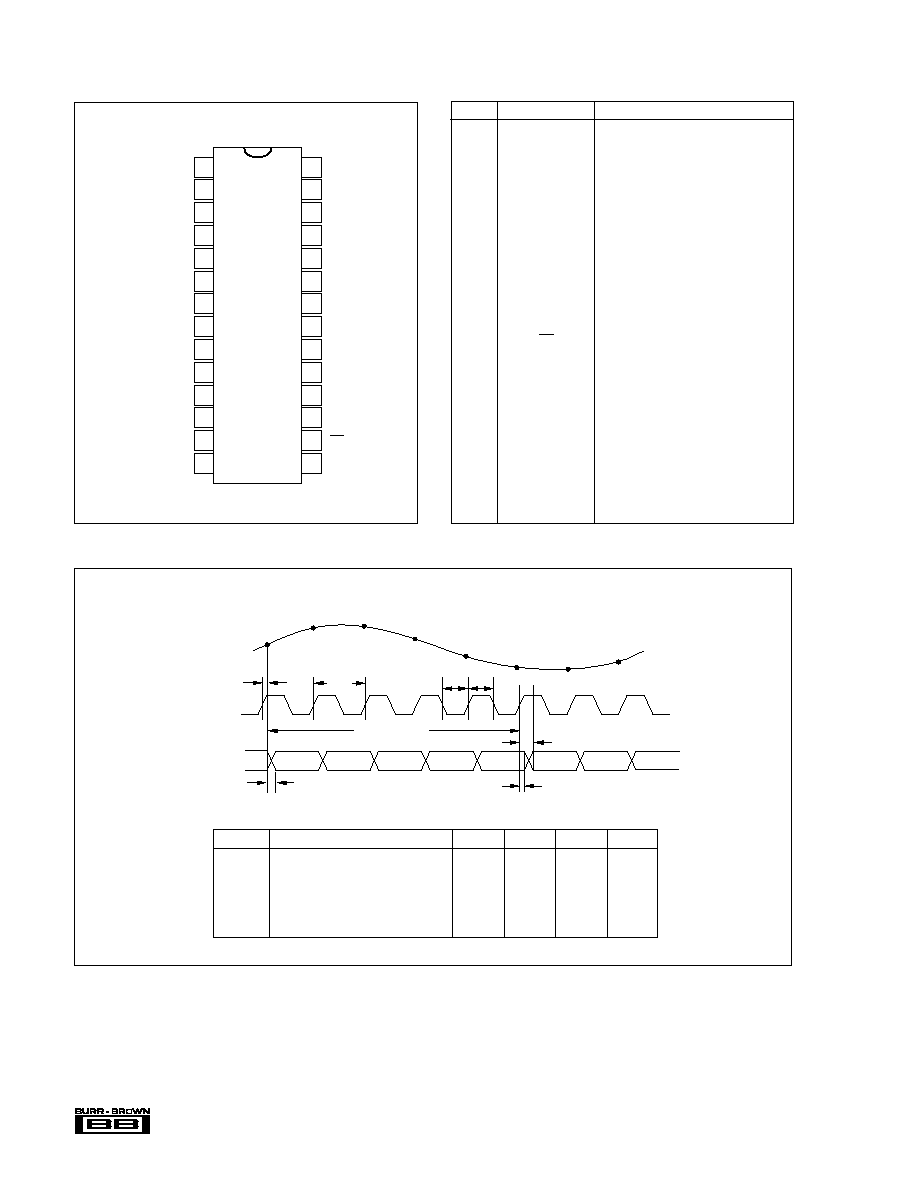
Top View
SSOP
PIN CONFIGURATION
PIN
DESIGNATOR
DESCRIPTION
1
+V
S
Analog Supply
2
LV
DD
Output Logic Driver Supply Voltage
3
NC
No Connection
4
NC
No Connection
5
Bit 8 (LSB)
Data Bit 8 (D7) LSB
6
Bit 7
Data Bit 7 (D6)
7
Bit 6
Data Bit 6 (D5)
8
Bit 5
Data Bit 5 (D4)
9
Bit 4
Data Bit 4 (D3)
10
Bit 3
Data Bit 3 (D2)
11
Bit 2
Data Bit 2 (D1)
12
Bit 1 (MSB)
Data Bit 1 (D0) MSB
13
GND
Analog Ground
14
GND
Analog Ground
15
CLK
Convert Clock Input
16
OE
Output Enable, Active Low
17
Pwrdn
Power Down Pin
18
+V
S
Analog Supply
19
GND
Analog Ground
20
GND
Analog Ground
21
LpBy
Positive Ladder Bypass
22
REFT
Reference Voltage Top
23
NC
No Connection
24
REFB
Reference Voltage Bottom
25
LnBy
Negative Ladder Bypass
26
CM
Common-Mode Pin
27
IN
Analog Input
28
+V
S
Analog Supply
PIN DESCRIPTIONS
TIMING DIAGRAM
SYMBOL
DESCRIPTION
MIN
TYP
MAX
UNITS
t
CONV
Convert Clock Period
33
100
µ
s
ns
t
L
Clock Pulse Low
15.5
16.5
ns
t
H
Clock Pulse High
15.5
16.5
ns
t
D
Aperture Delay
2
ns
t
1
Data Hold Time, C
L
= 0pF
3.9
ns
t
2
New Data Delay Time, C
L
= 15pF max
12
ns
5 Clock Cycles
Data Invalid
t
D
t
L
t
H
t
CONV
N≠5
N≠4
N≠3
N≠2
N≠1
N
N+1
N+2
Data Out
Clock
Analog In
N
t
2
N+1
N+2
N+3
N+4
N+5
N+6
N+7
t
1
+V
S
LV
DD
NC
NC
Bit 8 (LSB)
Bit 7
Bit 6
Bit 5
Bit 4
Bit 3
Bit 2
Bit 1 (MSB)
GND
GND
+V
S
IN
CM
LnBy
REFB
NC
REFT
LpBy
GND
GND
+V
S
Pwrdn
OE
CLK
ADS931
1
2
3
4
5
6
7
8
9
10
11
12
13
14
28
27
26
25
24
23
22
21
20
19
18
17
16
15
5
Æ
ADS931
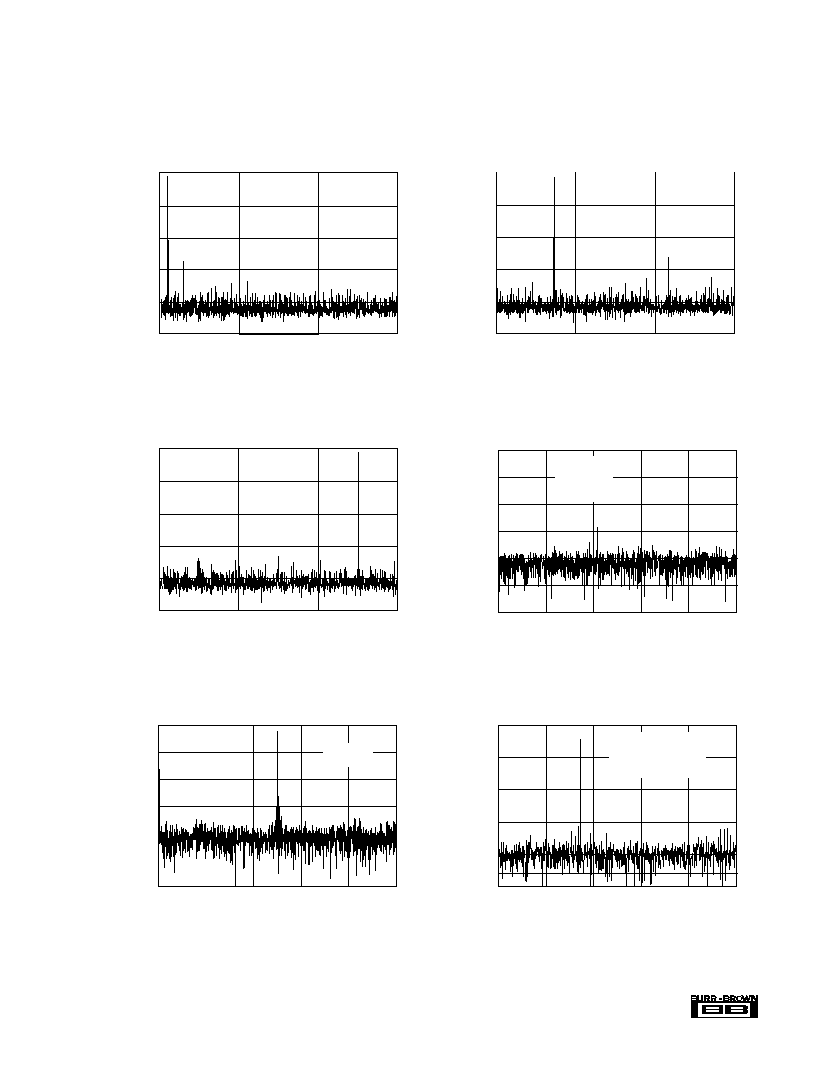
SPECTRAL PERFORMANCE
Frequency (MHz)
0
≠20
≠40
≠60
≠80
≠100
0
Amplitude (dB)
f
IN
= 3.58MHz
0
5
10
15
SPECTRAL PERFORMANCE
Frequency (MHz)
0
≠20
≠40
≠60
≠80
≠100
0
Amplitude (dB)
f
IN
= 12.5MHz
0
5
10
15
SPECTRAL PERFORMANCE
Frequency (MHz)
0
≠20
≠40
≠60
≠80
≠100
0
5
10
15
Amplitude (dB)
f
IN
= 500kHz
TYPICAL PERFORMANCE CURVES
At T
A
= +25
∞
C, V
S
= +3V, specified single-ended input (≠1dBFS) and sampling rate = 30MHz, unless otherwise specified.
SPECTRAL PERFORMANCE
Frequency (MHz)
0
≠20
≠40
≠60
≠80
≠100
≠120
0
3
6
12
9
15
Amplitude (dB)
f
IN
= 12.5MHz
V
S
= +5V
REFT
= +3.25V
REFB = +2.25V
UNDERSAMPLING PERFORMANCE
Frequency (MHz)
0
≠20
≠40
≠60
≠80
≠100
≠120
0
1.6
3.2
4.8
6.4
8.0
Amplitude (dB)
f
IN
= 20MHz
f
S
= 16MHz
TWO-TONE INTERMODULATION
Frequency (MHz)
0
≠20
≠40
≠60
≠80
≠100
0
2
4
8
6
10
Magnitude (dBFS)
f
1
= 3.6MHz at ≠7dB
f
2
= 3.5MHz at ≠7dB
2f
1
≠ f
2
55.7dBFS
2f
2
≠ f
1
54.6dBFS