 | –≠–ª–µ–∫—Ç—Ä–æ–Ω–Ω—ã–π –∫–æ–º–ø–æ–Ω–µ–Ω—Ç: AFE1115E | –°–∫–∞—á–∞—Ç—å:  PDF PDF  ZIP ZIP |
1
Æ
AFE1115
AFE1115
Æ
©
1997 Burr-Brown Corporation
PDS-1384
Printed in U.S.A. July, 1997
HDSL/MDSL ANALOG FRONT END WITH VCXO
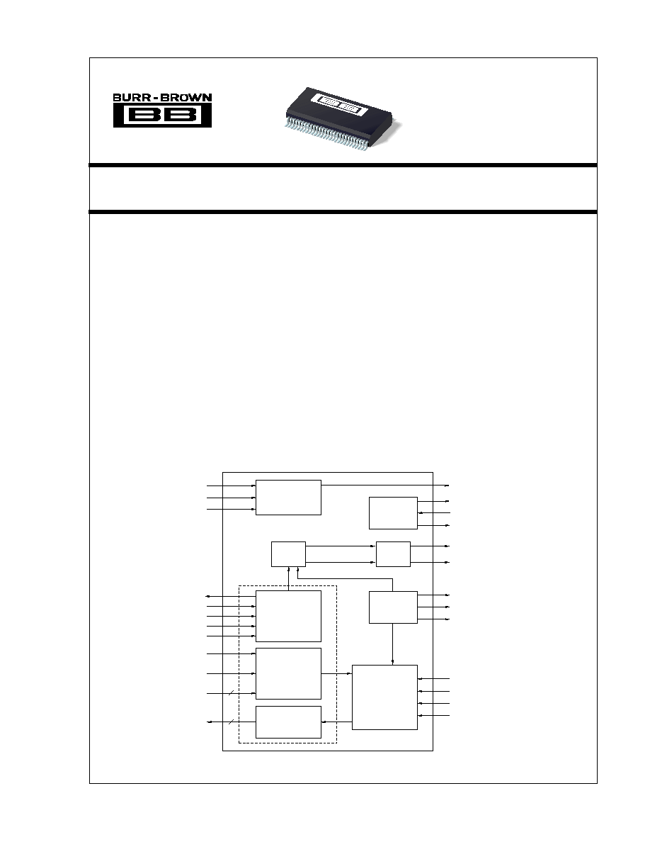
DESCRIPTION
Burr-Brown's Analog Front End greatly reduces the
size and cost of an HDSL (High bit rate Digital
Subscriber Line) system by providing all of the active
analog circuitry needed to connect an HDSL digital
signal processor to an external compromise hybrid and
a HDSL line transformer. The transmit and receive
filter responses automatically change with clock fre-
quency--allowing the AFE1115 to operate over a
range of data rates from 196kbps to 1.168Mbps.
Functionally, this unit consists of a transmit and a
receive section with a VCXO (Voltage Controlled
Crystal Oscillator) control DAC and VCXO circuitry.
The transmit section generates, filters, and buffers
outgoing 2B1Q data. The receive section filters and
digitizes the symbol data received on the telephone
line. Data to the VCXO and symbol data are sent to the
AFE1115 via two serial interfaces; the receive data is
available as a 14-bit parallel word. This IC operates on
a single 5V supply. The digital circuitry in the unit can
be connected to a supply from 3.3V to 5V. It is housed
in a small 56-pin SSOP package.
Pulse
Former
Filter
PLL
OUT
PLL
IN
txDATA+
txSCLK
txCLK
rxSYNC
rxLOOP
rxGAIN
rxDATA
Output
Buffer
Voltage
Reference
Delta-Sigma
Modulator
Transmit
Control
Receive
Control
Decimation
Filter
14
2
vcDATA
vcSCLK
vcLE
VCXO
DAC
txLINE≠
txLINE+
vcDAC
REF
P
V
CM
REF
N
Oscillator
VCXO Output
VCXO Input
VCXO Output Clock
rxLINE+
rxLINE≠
rxHYB+
rxHYB≠
Æ
AFE1115
International Airport Industrial Park ∑ Mailing Address: PO Box 11400, Tucson, AZ 85734 ∑ Street Address: 6730 S. Tucson Blvd., Tucson, AZ 85706 ∑ Tel: (520) 746-1111 ∑ Twx: 910-952-1111
Internet: http://www.burr-brown.com/ ∑ FAXLine: (800) 548-6133 (US/Canada Only) ∑ Cable: BBRCORP ∑ Telex: 066-6491 ∑ FAX: (520) 889-1510 ∑ Immediate Product Info: (800) 548-6132
q
+5V ONLY (5V or 3.3V Digital)
q
SCALEABLE DATA RATE
q
300mW POWER DISSIPATION
q
56-PIN SSOP
FEATURES
q
COMPLETE HDSL ANALOG INTERFACE
q
E1, T1 AND MDSL OPERATION
q
VCXO AND VCXO CONTROL CIRCUITRY

2
Æ
AFE1115
SPECIFICATIONS
Typical at 25
∞
C, AV
DD
= +5V, DV
DD
= +3.3V, f
tx
= 584kHz (E1 rate), unless otherwise specified.
AFE1115E
PARAMETER
COMMENTS
MIN
TYP
MAX
UNITS
RECEIVE CHANNEL
Number of Inputs
Differential
2
Input Voltage Range
Balanced Differential
(1)
±
3.0
V
Common-Mode Voltage
+2.5
V
Input Impedance All Inputs
See Typical Performance Curves
Input Capacitance
10
pF
Input Gain Matching
Line Input vs Hybrid Input
±
2
%
Resolution
14
Bits
Programmable Gain
Three Gains: ≠3dB, 3dB, and 9dB
≠3
+9
dB
Settling Time for Gain Change
6
Symbol Periods
Gain + Offset Error
Tested at Each Gain Range
5
%FSR
(2)
Output Data Coding
Two's Complement
Output Data Rate, rxSYNC
(3)
98
584
kHz
TRANSMIT CHANNEL
Transmit Clock Rate, f
tx
Symbol Rate
98
584
kHz
T1 Transmit ≠3dB Point
Bellcore TA-NWT-3017 Compliant
196
kHz
T1 Rate Power
(4, 5)
See Test Method Section
13
14
dBm
E1 Transmit ≠3dB Point
ETSI RTR/TM-03036 Compliant
292
kHz
E1 Transmit Power
(4, 5)
See Test Method Section
13
14
dBm
Pulse Output
See Typical Performance Curves
Common-Mode Voltage, V
CM
AV
DD
/2
V
Output Resistance
(6)
DC to 1MHz
1
TRANSCEIVER PERFORMANCE
Uncancelled Echo
(7)
rxGAIN = ≠3dB, Loopback Enabled
≠67
dB
rxGAIN = ≠3dB, Loopback Disabled
≠67
dB
rxGAIN = 3dB, Loopback Disabled
≠71
dB
rxGAIN = 9dB, Loopback Disabled
≠73
dB
VCXO PERFORMANCE
VCXO Control DAC Resolution
8
Bits
VCXO Control DAC Output
Positive Full Scale Output
4.5
V
VCXO Control DAC Output
Negative Full Scale Output
0.5
V
VCXO Performance
See VCXO Circuit and Layout Section
DIGITAL INTERFACE
(6)
Logic Levels
V
IH
|I
IH
| < 10
µ
A
DV
DD
≠1
DV
DD
+0.3
V
V
IL
|I
IL
| < 10
µ
A
≠0.3
+0.8
V
V
OH
I
OH
= ≠20
µ
A
DV
DD
≠0.5
V
V
OL
I
OL
= 20
µ
A
+0.4
V
POWER
Analog Power Supply Voltage
Specification
5
V
Analog Power Supply Voltage
Operating Range
4.75
5.25
V
Digital Power Supply Voltage
Specification
3.3
V
Digital Power Supply Voltage
Operating Range
3.15
5.25
V
Power Dissipation
(4, 5, 8)
AV
DD
= 5V, DV
DD
= 3.3V,
300
mW
Power Dissipation
(4, 5, 8)
AV
DD
= DV
DD
= 5V
350
mW
PSRR
60
dB
TEMPERATURE RANGE
Operating
(6)
≠40
+85
∞
C
NOTES: (1) With a balanced differential signal, the positive input is 180
∞
out of phase with the negative input, therefore the actual voltage swing about the common-
mode voltage on each pin is
±
1.5V to achieve a total input range of
±
3.0V or 6Vp-p. (2) FSR is Full-Scale Range. (3) The output data is available at twice the symbol
rate with interpolated values. (4) With a pseudo-random equiprobable sequence of HDSL pulses; 13.5dBm applied to the transformer (16.5dBm output from txLINEP
and txLINEN). (5) See the Test Method section of this data sheet for more information. (6) Guaranteed by design and characterization. (7) Uncancelled Echo is a
measure of the total analog errors in the transmitter and receiver sections including the effect of non-linearity and noise. See the Discussion of Specifications sections
of this data sheet for more information. (8) Power dissipation includes only the power dissipated with in the component and does not include power dissipated in the
external loads. See the Discussion of Specifications section for more information.
3
Æ
AFE1115
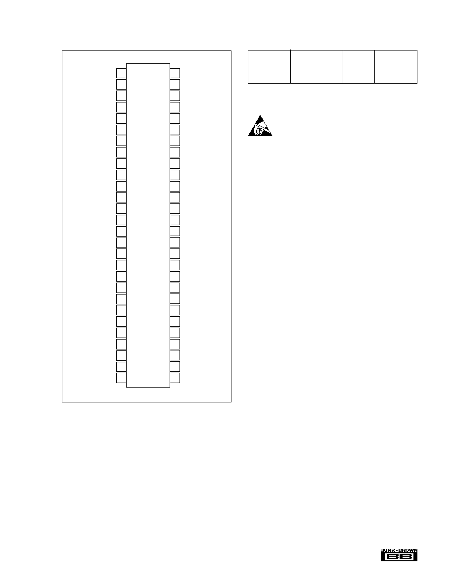
PIN CONFIGURATION
PACKAGE
DRAWING
TEMPERATURE
PRODUCT
PACKAGE
NUMBER
(1)
RANGE
AFE1115E
56-Pin Plastic SSOP
346
≠40
∞
C to +85
∞
C
NOTE: (1) For detailed drawing and dimension table, please see end of data
sheet, or Appendix C of Burr-Brown IC Data Book.
PACKAGE/ORDERING INFORMATION
ELECTROSTATIC
DISCHARGE SENSITIVITY
This integrated circuit can be damaged by ESD. Burr-Brown
recommends that all integrated circuits be handled with
appropriate precautions. Failure to observe proper handling
and installation procedures can cause damage.
ESD damage can range from subtle performance degradation
to complete device failure. Precision integrated circuits may
be more susceptible to damage because very small parametric
changes could cause the device not to meet its published
specifications.
vcOUT
vcINP
vcCLK
DVDD
Unused Pin
Unused Pin
txCLK
txSCLK
txDATA
rxDATA0
rxDATA1
rxDATA2
rxDATA3
rxDATA4
rxDATA5
GNDD
DV
DD
rxDATA6
rxDATA7
rxDATA8
rxDATA9
rxDATA10
rxDATA11
rxDATA12
rxDATA13
Unused Pin
rxSYNC
rxGAIN0
DGND
vcSCLK
vcDATA
vcLATCH
PLL
IN
PLL
OUT
AV
DD
AGND
AGND
vcDAC
AGND
txLINE+
AV
DD
txLINE≠
AGND
AV
DD
vrREF
V
CM
vrREF
AGND
AGND
rxLINE+
rxLINE≠
rxHYB+
rxHYB≠
AV
DD
rxLOOP
rxGAIN1
1
2
3
4
5
6
7
8
9
10
11
12
13
14
15
16
17
18
19
20
21
22
23
24
25
26
27
28
56
55
54
53
52
51
50
49
48
47
46
45
44
43
42
41
40
39
38
37
36
35
34
33
32
31
30
29
AFE1115E

4
Æ
AFE1115
PIN #
TYPE
NAME
DESCRIPTION
1
Output
vcOUT
VCXO Output
2
Input
vcINP
VCXO Input
3
Output
vcCLK
VCXO Output Clock
4
Power
DVDD
Digital Supply (+3.3 to +5V)
5
NC
Unused Pin
6
NC
Unused Pin
7
Input
txCLK
Transmit Baud Clock (XMTLE signal) (1168kHz for E1)
8
Input
txSCLK
Transmit Serial Clock
9
Input
txDATA
Transmit Data Input
10
Output
rxDATA0
ADC Output Bit-0
11
Output
rxDATA1
ADC Output Bit-1
12
Output
rxDATA2
ADC Output Bit-2
13
Output
rxDATA3
ADC Output Bit-3
14
Output
rxDATA4
ADC Output Bit-4
15
Output
rxDATA5
ADC Output Bit-5
16
Ground
GNDD
Digital Ground
17
Power
DV
DD
Digital Supply (+3.3 to +5V)
18
Output
rxDATA6
ADC Output Bit-6
19
Output
rxDATA7
ADC Output Bit-7
20
Output
rxDATA8
ADC Output Bit-8
21
Output
rxDATA9
ADC Output Bit-9
22
Output
rxDATA10
ADC Output Bit-10
23
Output
rxDATA11
ADC Output Bit-11
24
Output
rxDATA12
ADC Output Bit-12
25
Output
rxDATA13
ADC Output Bit-13
26
NC
Unused Pin
(DV
DD
may be connected for pinout compatibility with AFE1105)
27
Input
rxSYNC
ADC Sync Signal (392kHz for T1, 584kHz for E1)
28
Input
rxGAIN0
Receive Gain Control Bit-0
29
Input
rxGAIN1
Receive Gain Control Bit-1
30
Input
rxLOOP
Loopback Control Signal (loopback is enabled by positive signal)
31
Power
AV
DD
Analog Supply (+5V)
32
Input
rxHYB≠
Negative Input from Hybrid Network
33
Input
rxHYB+
Positive Input from Hybrid Network
34
Input
rxLINE≠
Negative Line Input
35
Input
rxLINE+
Positive Line Input
36
Ground
AGND
Analog Ground
37
Ground
AGND
Analog Ground
38
Output
vrREFP
Positive Reference Output
39
Output
V
CM
Common-mode Voltage (buffered)
40
Output
vrREFN
Negative Reference Output
41
Power
AV
DD
Analog Supply (+5V)
42
Ground
AGND
Analog Ground
43
Output
txLINE≠
Negative Line Output
44
Power
AV
DD
Analog Supply (+5V)
45
Output
txLINE+
Positive Line Output
46
Ground
AGND
Analog Ground
47
Output
vcDAC
VCXO Control
48
Ground
AGND
Analog Ground
49
Ground
AGND
PLL Ground
50
Power
AV
DD
PLL Supply
51
Output
PLL
OUT
PLL Filter Output
52
Input
PLL
IN
PLL Filter Input
53
Input
vcLATCH
VCXO Control Latch Enable
54
Input
vcDATA
VCXO Control Data
55
Input
vcSCLK
VCXO Control Serial Clock
56
Ground
DGND
Digital Ground
The information provided herein is believed to be reliable; however, BURR-BROWN assumes no responsibility for inaccuracies or omissions. BURR-BROWN
assumes no responsibility for the use of this information, and all use of such information shall be entirely at the user's own risk. Prices and specifications are subject
to change without notice. No patent rights or licenses to any of the circuits described herein are implied or granted to any third party. BURR-BROWN does not
authorize or warrant any BURR-BROWN product for use in life support devices and/or systems.
PIN DESCRIPTIONS
5
Æ
AFE1115
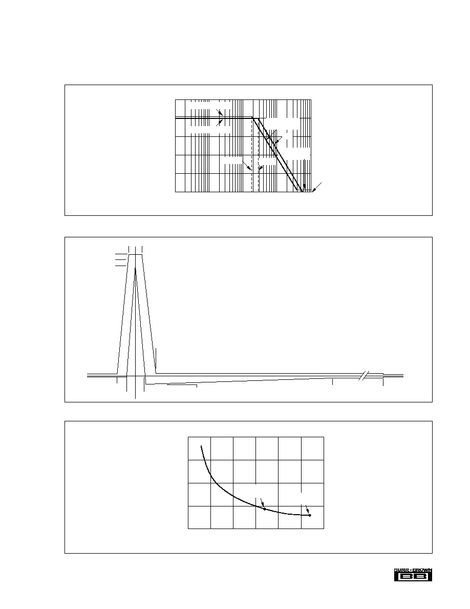
100
200
150
100
50
0
300
500
INPUT IMPEDANCE vs BIT RATE
Input Impedance (k
)
Bit Rate (kbps)
700
900
1300
1100
T1 = 784kbps,
45k
E1 = 1168kbps,
30k
1K
≠20
≠40
≠60
≠80
≠100
≠120
10K
100K
POWER SPECTRAL DENSITY LIMIT
Power Spectral Density (dBm/Hz)
Frequency (Hz)
1M
10M
≠38dBm/Hz for T1
≠40dBm/Hz for E1
196kHz
292kHz
≠80dB/decade
T1
≠120dBm/Hz
for E1
≠118dBm/Hz
for T1
E1
TYPICAL PERFORMANCE CURVES
At Output of Pulse Transformer
The curves shown below are measured at the line output of the HDSL transformer. Typical at 25
∞
C, AV
DD
= +5V, DV
DD
= +3.3V, unless otherwise specified.
CURVE 2. Transmitted Pulse Template and Actual Performance as Measured at Transformer Output.
CURVE 1. Upper Bound of Power Spectral Density Measured at Output of HDSL Transformer.
CURVE 3. Input Impedance of rxLINE and rxHYB.
0.4T
B = 1.07
C = 1.00
D = 0.93
0.4T
≠0.6T
≠1.2T
A = 0.01
E = 0.03
G = ≠0.16
A
B
C
D
E
F
G
H
0.01
1.07
1.00
0.93
0.03
≠0.01
≠0.16
≠0.05
0.0264
2.8248
2.6400
2.4552
0.0792
≠0.0264
≠0.4224
≠0.1320
≠0.0264
≠2.8248
≠2.6400
≠2.4552
≠0.0792
0.0264
0.4224
0.1320
0.0088
0.9416
0.8800
0.8184
0.0264
≠0.0088
≠0.1408
≠0.0440
≠0.0088
≠0.9416
≠0.8800
≠0.8184
≠0.0264
0.0088
0.1408
0.0440
NORMALIZED
LEVEL
QUATERNARY SYMBOLS
DON'T DELETE TABLE
UNTIL KNOWN IF TEEPLE IS LEAVING IT IN?
+3
≠3
+1
≠1
14T
H = ≠0.05
50T
F = ≠0.01
A = 0.01
F = ≠0.01
0.5T
1.25T