 | ÐлекÑÑоннÑй компоненÑ: AFE8201 | СкаÑаÑÑ:  PDF PDF  ZIP ZIP |
Äîêóìåíòàöèÿ è îïèñàíèÿ www.docs.chipfind.ru
FEATURES
D
12-BIT, 80MSPS ADC
D
INTEGRATED DIGITAL DOWNCONVERTER (DDC):
Quadrature Mixer/NCO
CIC Decimation Filter
FIR Filters
D
MIXER: 32-BIT FREQUENCY AND PHASE
D
DECIMATION RATIO: 32 to 4096
D
USER PROGRAMMABLE FIR FILTERS WITH
16-BIT COEFFICIENTS
D
12-BIT AUXILIARY DAC
D
DATA INTERFACE COMPATIBLE WITH TI C5x/C6x
DSP BUFFERED SERIAL PORT (McBSP):
Code Composer Module for Easy Software
Generation
D
SPI
CONTROL INTERFACE
D
3.3V ANALOG, 1.8V DIGITAL SUPPLY
D
1.8V to 3.3V I/O SUPPLY
D
TQFP-48
APPLICATIONS
D
SOFTWARE RADIOS
D
IF RECEIVE CHANNEL
D
DIGITAL RADIO RECEIVERS
D
NARROWBAND RECEIVERS
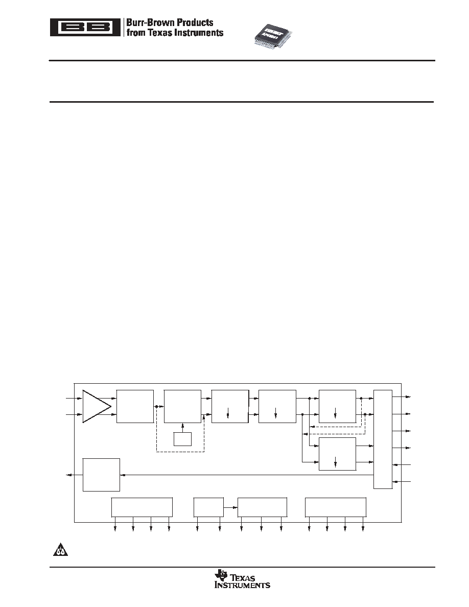
DESCRIPTION
The AFE8201 consists of a general-purpose, 80MSPS,
12-bit analog-to-digital converter (ADC), a digital
downconverter (DDC), and user-programmable digital
filters. It is designed to sample narrowband (2.5MHz or
less) IF signals and digitally mix, filter, and decimate the
signals to baseband.
The DDC consists of a digital quadrature mixer followed
by a CIC decimation filter and FIR filters. The mixer
frequency and initial phase are independently
programmed by 32-bit control words.
After the CIC filter, the internal I and Q signals are
passed on to the first FIR filter, which can implement
even, odd, halfband, and arbitrary impulse responses
with up to 62 taps using 16-bit coefficients.
Following the first FIR filter are two parallel FIR filters
that can be used to provide two output streams or
interleaved to form one extended filter with up to 262
taps. The AFE8201 also contains a 12-bit
general-purpose auxiliary digital-to-analog converter
(DAC) for applications such as AGC amplifier control.
Control register data as well as decimation filter
coefficients are written to the AFE8201 through the
industry-standard SPI control interface. The baseband
output signals are transported through a general-
purpose, high-speed serial interface that is compatible
with TI C5x/C6x DSP family buffered serial ports
(McBSP).
12-Bit
Pipeline
ADC
Auxiliary
DAC
Voltage
Reference
AUX
IFM
IFP
Quadrature
Mixer
NCO
CIC Filter
FIR Filter 1
FIR Filter 2A
Data
I
n
ter
f
ac
e
DOUT0
DOUT1
DFSO
DCLK
DIN
DFSI
FIR Filter 2B
N
2
2
2
REFM VCM REFP
VGB
SPI Control
Interface
SCK
MOSI MISO CS_N
Timing
Generator
PWD
SYNC RST_N
Clock
Interface
MCLK
MCLKB
PRODUCT PREVIEW
AFE8201
SBWS016A - OCTOBER 2003 - REVISED JANUARY 2005
IF Analog-to-Digital Converter
with Digital Downconverter
www.ti.com
Copyright
2003-2005, Texas Instruments Incorporated
Please be aware that an important notice concerning availability, standard warranty, and use in critical applications of Texas Instruments
semiconductor products and disclaimers thereto appears at the end of this data sheet.
All trademarks are the property of their respective owners.
PRODUCT PREVIEW information concerns products in the formative or design
phase of development. Characteristic data and other specifications are design
goals. Texas Instruments reserves the right to change or discontinue these
products without notice.
AFE8201
SBWS016A - OCTOBER 2003 - REVISED JANUARY 2005
www.ti.com
2
ORDERING INFORMATION
(1)
PRODUCT
PACKAGE-LEAD
PACKAGE
DESIGNATOR
SPECIFIED
TEMPERATURE
RANGE
PACKAGE
MARKING
ORDERING
NUMBER
TRANSPORT MEDIA,
QUANTITY
AFE8201
TQFP-48
PFB
-40
°
C to +85
°
C
AFE8201
AFE8201PFBT
Tape and Reel, 250
AFE8201
TQFP-48
PFB
-40
°
C to +85
°
C
AFE8201
AFE8201PFBR
Tape and Reel, 2000
(1) For the most current package and ordering information, see the Package Option Addendum located at the end of this data sheet, or see the
TI web site at www.ti.com.
ABSOLUTE MAXIMUM RATINGS
over operating free-air temperature range unless otherwise noted(1)
Supply Voltage Range:
AVDD
-0.5V to 4V
. . . . . . . . . . . . . . . . . . . . . . . . . . . . . . . . . . . . .
DVDD
-0.5V to 2.3V
. . . . . . . . . . . . . . . . . . . . . . . . . . . . . . . . . . .
IOVDD
-0.5V to 3.6V
. . . . . . . . . . . . . . . . . . . . . . . . . . . . . . . . . .
Voltage Between AGND and DGND
-0.3V to 0.5V
. . . . . . . . . . . . .
Voltage Between AVDD to DVDD
-3.3V to 3.3V
. . . . . . . . . . . . . . .
Digital Inputs(2)
-0.3V to DVDD + 0.3V
. . . . . . . . . . . . . . . . . . . . . . .
Digital Output Data
-0.3V to DVDD + 0.3V
. . . . . . . . . . . . . . . . . . . .
Operating Free-Air Temperature Range. TA
-40
°
C to 85
°
C
. . . . . .
Storage Temperature Range
-55
°
C to +125
°
C
. . . . . . . . . . . . . . . . .
(1) Stresses beyond those listed under Absolute Maximum Ratings
may cause permanent damage to the device. These are stress
ratings only; functional operation of the device at these or any
other conditions beyond those indicated under the
Recommended Operating Conditions is not implied. Exposure to
absolute-maximum-rated conditions for extended periods may
affect device reliability.
(2) Measured with respect to DGND.
This integrated circuit can be damaged by ESD. Texas
Instruments recommends that all integrated circuits be
handled with appropriate precautions. Failure to observe
proper handling and installation procedures can cause damage.
ESD damage can range from subtle performance degradation to
complete device failure. Precision integrated circuits may be more
susceptible to damage because very small parametric changes could
cause the device not to meet its published specifications.
RECOMMENDED OPERATING CONDITIONS
MIN
TYP
MAX
UNITS
Supplies and References
Operating Free-Air Temperature, TA
-40
85
°
C
Analog Supply Voltage, AVDD
3.15
3.3
3.45
V
Digital Supply Voltage, DVDD
1.6
1.8
2.0
V
Output Driver Supply Voltage, IOVDD
1.6
3.6
V
Input Common-Mode Voltage
VCM
V
Differential Input Voltage Range
2
VPP
Clock Inputs: MCLK and MCLKB
Sample Rate, fS
5
80
MHz
Differential Input Mode Voltage Input Swing
0.4
3.3
V
Differential Input Common-Mode Voltage
1.65
V
Single-Ended Mode High-Level Input Voltage, VIHC
2
V
Single-Ended Mode Low-Level Input Voltage, VILC
0.8
V
Clock Pulse Width High, tW(H)
5.625
6.25
ns
Clock Pulse Width Low, tW(L)
5.625
6.25
ns
Digital Inputs
High-Level Input Voltage, VIH
0.7
×
IOVDD
V
Low-Level Input Voltage, VIL
0.25
×
IOVDD
V
PRODUCT PREVIEW
AFE8201
SBWS016A - OCTOBER 2003 - REVISED JANUARY 2005
www.ti.com
3
AUXILIARY DAC CHARACTERISTICS
All specifications at +25
°
C, AVDD = +3.3V, and DVDD = +1.8V, unless otherwise noted.
PARAMETER
CONDITIONS
MIN
TYP
MAX
UNIT
Resolution
12
bits
Output voltage range
Input code 0x000
0.0
V
Output voltage range
Input code 0xFFF
2.75
V
Output impedance
1
k
Settling time
to 0.1% FSR
10
µ
s
Offset
±
1
% of FSR
DC
Gain error
±
5
% of FSR
DC
performance
Differential nonlinearity, DNL
Ensured monotonic
±
0.5
LSB
performance
Integral nonlinearity, INL
After correcting for gain and offset errors
±
2
LSB
Power-supply rejection ratio, PSRR
Input code 0x400, AVDD = 3.15VDC to 3.45VDC
60
dB
RECEIVE CHANNEL CHARACTERISTICS
All specifications at +25
°
C, fS = 80MSPS, AVDD = +3.3V, DVDD = +1.8V, IOVDD = +3.3V, Gain = 1, Decimation Ratio = 80, Internal Digital
Filter Bandwidth = 264kHz, and Input Signal = 10.7MHz, unless otherwise noted.
PARAMETER
CONDITIONS
MIN
TYP
MAX
UNIT
DC Accuracy
Input impedance
6.25
k
Differential nonlinearity, DNL
-0.0244
±
0.0122
+0.0244
%FSR
Integral nonlinearity, INL
-0.0244
±
0.012
+0.0244
%FSR
Offset error
3
mV
Gain error
1
%FS
Gain = 1
1.0
V
Gain = 1.14
0.875
V
Gain = 1.33
0.75
V
Full-scale input level (peak differential)
Gain = 1.6
0.625
V
Full-scale input level (peak differential)
Gain = 2.0
0.5
V
Gain = 2.67
0.375
V
Gain = 4.0
0.25
V
Gain change settling time
Number of samples to achieve rated accuracy
2
Samples
Power-supply rejection ratio, PSRR
AVDD = 3.15VDC to 3.45VDC
70
dB
References
Negative reference, VREFN
1.1
1.25
1.4
V
Positive reference, VREFP
2.1
2.25
2.4
V
Common-mode voltage, VCM
1.8
V
AC Performance
Spurious-free dynamic range, SFDR
Input 455kHz, -1dBFS
76
dBc
Spurious-free dynamic range, SFDR
Input 10.7MHz, -1dBFS
76
86
dBc
2nd-order harmonic, HD2
Input 10.7MHz, -1dBFS
80
dBc
Input 455kHz, -1dBFS
75
dB
Signal-to-noise ratio, SNR
Input 10.7MHz, -1dBFS
70
74
dB
Signal-to-noise ratio, SNR
In 3kHz bandwidth, -1dBFS, 10.7MHz, 20kHz from fundamental
102
dB
Aperture delay
2
ns
Aperture uncertainty
0.2
ps
Power Supply
Analog supply voltage, AVDD
3.15
3.3
3.45
V
Digital supply voltage, DVDD
1.71
1.8
1.89
V
Output driver supply voltage, IOVDD
3.15
3.3
3.45
V
Power dissipation
Normal operation
490
570
mW
Power dissipation
Power-down
20
mW
Digital I/O supply current
7
mA
Digital supply current
72
mA
Analog supply current
103
mA
PRODUCT PREVIEW
AFE8201
SBWS016A - OCTOBER 2003 - REVISED JANUARY 2005
www.ti.com
4
DIGITAL INTERFACE SPECIFICATIONS
All specifications at +25
°
C, AVDD = 3.3V, DVDD = 1.8V, and VDDS = 3.3V, unless otherwise noted.
PARAMETER
CONDITIONS
MIN
TYP
MAX
UNITS
High Level Input Current, IIH
VIH = 1.6V to 3.6V
-10
10
µ
A
Low-Level Input Current, IIL
VIL = 0V to 0.4V
-10
10
µ
A
High-Level Output Voltage, VOH
IOH = -50
µ
A
0.8
×
IOVDD
V
Low-Level Output Voltage, VOL
IOL = 50
µ
A
0.2
×
IOVDD
V
DATA INTERFACE TIMING
DCLKO
DFSO
DOUT0
DOUT1
IA[15]
IA[14]
IA[13]
IA[12]
IB[15]
IB[14]
IB[13]
IB[12]
t
d1
t
d2
t
d3
Figure 1. Data Interface Timing 1
PARAMETER
CONDITIONS
MIN
TYP
MAX
UNITS
DCLKO to DFSO Delay, td1
-0.4
3.2
ns
DCLKO to DOUT0 Delay, td2
-0.2
2.5
ns
DCLKO to DOUT1 Delay, td3
-0.2
2.5
ns
DCLKO
DFSI
DIN
D[15]
D[14]
D[13]
D[12]
t
su1
t
su2
t
h1
t
h2
Figure 2. Data Interface Timing 2
PARAMETER
CONDITIONS
MIN
TYP
MAX
UNITS
DFSI to DCLKO Setup Time, tsu1
1.2
ns
DFSI to DCLKO Hold Time, th1
0.4
ns
DIN to DCLKO Setup Time, tsu2
1.0
ns
DIN to DCLKO Hold Time, th2
0.4
ns
PRODUCT PREVIEW
AFE8201
SBWS016A - OCTOBER 2003 - REVISED JANUARY 2005
www.ti.com
5
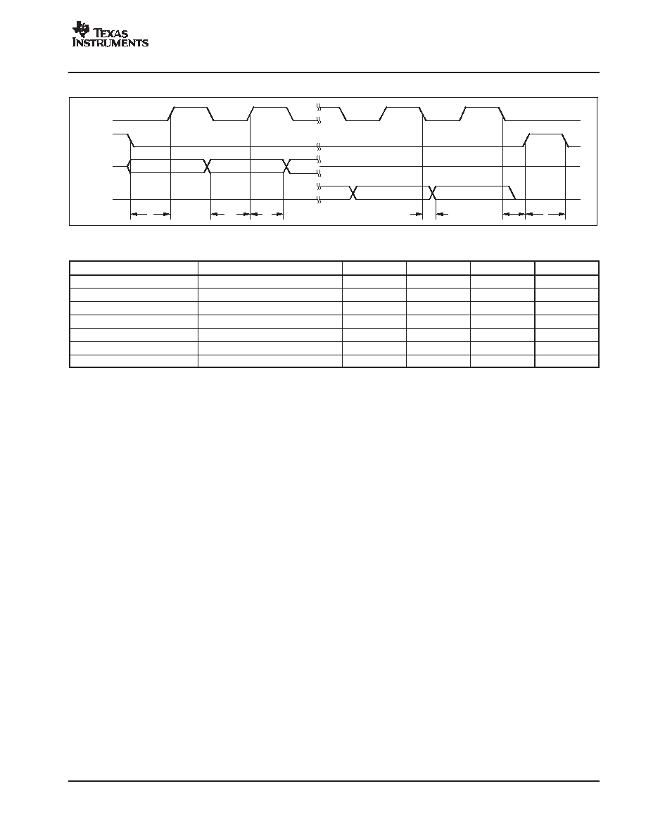
CONTROL INTERFACE TIMING
SCK
CS_N
MOSI
MISO
t
L
t
su3
t
h3
t
T
t
I
t
d4
Figure 3. Control Interface Timing
PARAMETER
CONDITIONS
MIN
TYP
MAX
UNITS
Maximum SCK Frequency
1
MHz
CS_N Leading Time, tL
Trailing CS_N to Leading SCK
5.0
ns
CS_N Trailing Time, tT
Trailing SCK to Leading CS_N
5.0
ns
CS_N Idle Time, tL
5.0
ns
MOSI to SCK Setup Time, tsu3
Leading CS_N to Trailing CS_N
5.0
ns
MOSI to SCK Hold Time, th3
1.0
ns
SCK to MISO Delay Time, td4
1.0
8.0
ns
PRODUCT PREVIEW