FEATURES
D
Interfaces To Texas Instruments DRIx50 HD
Radio Baseband Processors
D
12-Bit, 80MSPS ADC Reduces Noise and
Improves Sensitivity
D
Typical SNR of 102dB in 3kHz Bandwidth
D
Programmable Input Range For Optimum
Tuner Dynamic Range
D
Integrated Digital Downconverter (DDC)
- Quadrature Mixer, NCO, CIC Decimation
Filter, And FIR Filters
D
Mixer: 32-Bit Frequency and Phase
D
Decimation Ratio: 32 to 4096
D
User-Programmable FIR Filters with 16-Bit
Coefficients
D
12-Bit Auxiliary DAC
D
Code Composer Module for Easy Software
Generation
D
SPI
Control Interface
APPLICATIONS
D
AM/FM and HD Radio Receivers
D
IF Receive Channels
D
Software Radios
D
Narrowband Receivers
DESCRIPTION
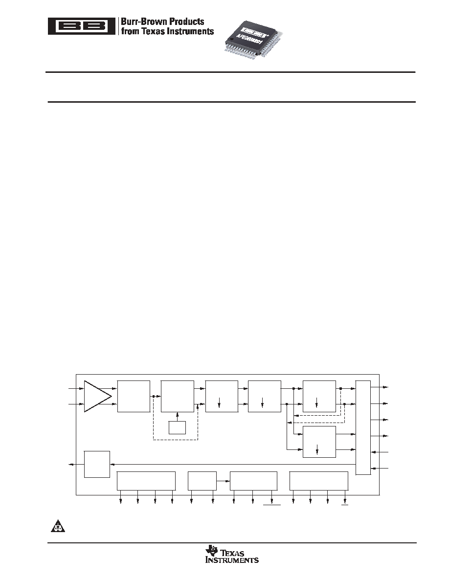
The AFEDRI8201 implements the receive channel analog
functions required for intermediate-frequency (IF)
sampled AM/FM and HD digital radio receivers. It is
designed to be used with TI's DRIx50 digital baseband
processor. The AFEDRI8201 is programmed by the
DRIx50 for use in AM/FM and HD radio. The AFEDRI8201
oversamples the radio tuner IF output at speeds of up to
80MHz to reduce noise and improve dynamic range. The
radio tuner output IF is typically 10.7MHz for AM or FM as
well as 450kHz or 455kHz for AM, as desired. The
AFEDRI8201 then mixes, filters, and decimates the signal
to provide baseband I and Q output signals to the digital
baseband processor. The AFEDRI8201 also includes a
general-purpose 12-bit control digital-to-analog converter
(DAC) to provide a gain control signal or other analog
feedback to the tuner.
The DRIx50 digital baseband device writes control register
data as well as decimation filter coefficients to the
AFEDRI8201 through the industry-standard SPI control
interface. The baseband output signals are transported to
the DRIx50 through a general-purpose, high-speed serial
interface (TI's Buffered Serial Ports, McBSP).
This unit uses 3.3V analog and 1.8V digital power
supplies. Typical power dissipation is 490mW. The digital
I/O lines can be powered by a 3.3V supply.
12-Bit
Pipeline
ADC
Auxiliary
DAC
Voltage
Reference
AUX
IFM
IFP
Quadrature
Mixer
NCO
CIC Filter
FIR Filter 1
FIR Filter 2A
D
a
ta
I
n
te
r
f
ac
e
DOUT0
DOUT1
DFSO
DCLK
DIN
DFSI
FIR Filter 2B
N
2
2
2
REFM VCM REFP
VGB
SPI Control
Interface
SCK
MOSI MISO
CS
Timing
Generator
PWD
SYNC RESET
Clock
Interface
MCLK
MCLKB
PRODUCTION DATA information is current as of publication date. Products
conform to specifications per the terms of Texas Instruments standard warranty.
Production processing does not necessarily include testing of all parameters.
AFEDRI8201
SBWS017F - SEPTEMBER 2003 - REVISED AUGUST 2005
IF ADC Front End for AM/FM and HD Radios
www.ti.com
Copyright
2003-2005, Texas Instruments Incorporated
Please be aware that an important notice concerning availability, standard warranty, and use in critical applications of Texas Instruments
semiconductor products and disclaimers thereto appears at the end of this data sheet.
SPI is a trademark of Motorola, Inc. All other trademarks are the property of their respective owners.
AFEDRI8201
SBWS017F - SEPTEMBER 2003 - REVISED AUGUST 2005
www.ti.com
2
ORDERING INFORMATION
(1)
PRODUCT
PACKAGE-LEAD
PACKAGE
DESIGNATOR
SPECIFIED
TEMPERATURE
RANGE
PACKAGE
MARKING
ORDERING
NUMBER
TRANSPORT MEDIA,
QUANTITY
AFEDRI8201
TQFP-48
PFB
-40
�
C to +85
�
C
DRI8201
AFEDRI8201PFBT
Tape and Reel, 250
AFEDRI8201
TQFP-48
PFB
-40
�
C to +85
�
C
DRI8201
AFEDRI8201PFBR
Tape and Reel, 2000
(1) For the most current package and ordering information, see the Package Option Addendum at the end of this data sheet, or see the TI website
at www.ti.com
This integrated circuit can be damaged by ESD. Texas Instruments recommends that all integrated circuits be handled with appropriate
precautions. Failure to observe proper handling and installation procedures can cause damage.
ESD damage can range from subtle performance degradation to complete device failure. Precision integrated circuits may be more susceptible to
damage because very small parametric changes could cause the device not to meet its published specifications.
ABSOLUTE MAXIMUM RATINGS
over operating free-air temperature range unless otherwise noted
(1)
AFEDRI8201
UNIT
AVDD
-0.5 to 4.0
V
Supply Voltage Range
DVDD
-0.5 to 2.3
V
Supply Voltage Range
IOVDD
-0.5 to 3.6
V
Voltage between AGND and DGND
-0.3 to 0.5
V
Voltage between AVDD and DVDD
-3.3 to 3.3
V
Digital inputs(2)
-0.3 to DVDD + 0.3
V
Digital data output
-0.3 to DVDD + 0.3
V
Operating free-air temperature range, T
A
-40 to +85
�
C
Storage temperature range
-55 to +125
�
C
(1) Stresses above these ratings may cause permanent damage. Exposure to absolute maximum conditions for extended periods may degrade
device reliability. These are stress ratings only, and functional operation of the device at these or any other conditions beyond those specified
is not implied.
(2) Measured with respect to DGND.
RECOMMENDED OPERATING CONDITIONS
MIN
TYP
MAX
UNIT
Operating free-air temperature range, T
A
-40
+85
�
C
Analog supply voltage range, AVDD
3.15
3.3
3.45
V
Supplies and
Digital supply voltage range, DVDD
1.71
1.8
1.89
V
Supplies and
References
Output driver supply voltage range, IOVDD
3.15
3.3
3.45
V
References
Input common-mode voltage
V
CM
V
Differential input voltage
2
V
PP
Sample rate, f
S
5
80
MHz
Differential input mode voltage input swing
0.4
3.3
V
Clock Inputs:
Single-ended mode high-level input voltage, V
IHC
2
V
Clock Inputs:
MCLK and MCLKB
Single-ended mode low-level input voltage, V
ILC
0.8
V
MCLK and MCLKB
Clock pulse width high, t
W(H)
5.625
6.25
ns
Clock pulse width low, t
W(L)
5.625
6.25
ns
AFEDRI8201
SBWS017F - SEPTEMBER 2003 - REVISED AUGUST 2005
www.ti.com
3
AUXILIARY DAC CHARACTERISTICS
All specifications at +25
�
C, AVDD = +3.3V, and DVDD = +1.8V, unless otherwise noted.
PARAMETER
CONDITIONS
MIN
TYP
MAX
UNIT
Resolution
12
bits
Output voltage range
Input code 0x000
0.0
V
Output voltage range
Input code 0xFFF
2.75
V
Output impedance
1
k
Settling time
to 0.1% FSR
10
�
s
Offset
�
1
% of FSR
DC
Gain error
�
5
% of FSR
DC
performance
Differential nonlinearity, DNL
Ensured monotonic
�
0.5
LSB
performance
Integral nonlinearity, INL
After correcting for gain and offset errors
�
2
LSB
Power-supply rejection ratio, PSRR
Input code 0x400, AVDD = 3.15VDC to 3.45VDC
60
dB
RECEIVE CHANNEL CHARACTERISTICS
All specifications at +25
�
C, f
S
= 80MSPS, AVDD = +3.3V, DVDD = +1.8V, IOVDD = +3.3V, Gain = 1, Decimation Ratio = 80, Internal Digital
Filter Bandwidth = 284kHz, and Input Signal = 10.7MHz, unless otherwise noted.
PARAMETER
CONDITIONS
MIN
TYP
MAX
UNIT
DC Accuracy
Input impedance
6.25
k
Differential nonlinearity, DNL
-0.0244
�
0.0122
+0.0244
%FSR
Integral nonlinearity, INL
-0.0244
�
0.012
+0.0244
%FSR
Offset error
3
mV
Gain error
1
%FS
Gain = 1
1.0
V
Gain = 1.14
0.875
V
Gain = 1.33
0.75
V
Full-scale input level (peak differential)
Gain = 1.6
0.625
V
Full-scale input level (peak differential)
Gain = 2.0
0.5
V
Gain = 2.67
0.375
V
Gain = 4.0
0.25
V
Gain change settling time
Number of samples to achieve rated accuracy
2
Samples
Power-supply rejection ratio, PSRR
AVDD = 3.15VDC to 3.45VDC
70
dB
References
Negative reference, VREFN
1.1
1.25
1.4
V
Positive reference, VREFP
2.1
2.25
2.4
V
Common-mode voltage, VCM
1.8
V
AC Performance
Spurious-free dynamic range, SFDR
Input 455kHz, -1dBFS
76
dBc
Spurious-free dynamic range, SFDR
Input 10.7MHz, -1dBFS
76
86
dBc
Input 455kHz, -1dBFS
75
dB
Signal-to-noise ratio, SNR
Input 10.7MHz, -1dBFS
70
74
dB
Signal-to-noise ratio, SNR
In 3kHz bandwidth, -1dBFS, 10.7MHz, 20kHz from fundamental
102
dB
Aperture delay
2
ns
Aperture uncertainty
0.2
ps
Power Supply
Analog supply voltage, AVDD
3.15
3.3
3.45
V
Digital supply voltage, DVDD
1.71
1.8
1.89
V
Output driver supply voltage, IOVDD
3.15
3.3
3.45
V
Power dissipation
Normal operation
490
570
mW
Power dissipation
Power-down
20
mW
Digital I/O supply current
7
mA
Digital supply current
72
mA
Analog supply current
103
mA
AFEDRI8201
SBWS017F - SEPTEMBER 2003 - REVISED AUGUST 2005
www.ti.com
4
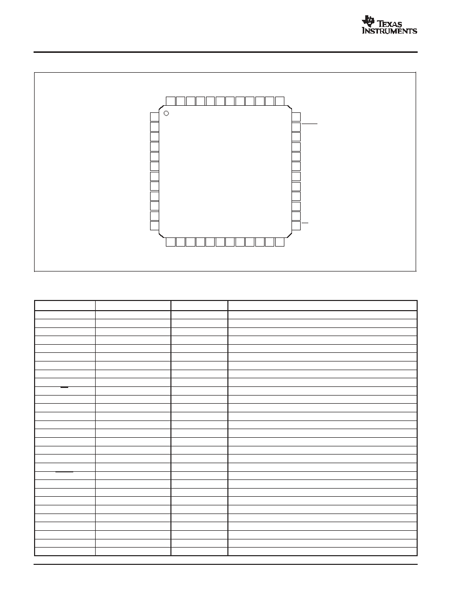
PIN ASSIGNMENTS
36
35
34
33
32
31
30
29
28
27
26
25
SYNC
RESET
DOUT1
DOUT0
DCLK
DFSO
DIN
DFSI
SCK
MISO
MOSI
CS
AVD
D
AG
N
D
AVD
D
AVD
D
AG
N
D
AG
N
D
DG
N
D
DV
D
D
IO
G
N
D
IO
V
D
D
IO
G
N
D
PWD
AV
D
D
AU
X
AG
N
D
NC
AG
N
D
MC
LK
MC
LK
B
AV
D
D
DG
ND
DV
DD
IO
G
N
D
IO
V
D
D
1
2
3
4
5
6
7
8
9
10
11
12
AVDD
AGND
IFP
IFM
AGND
VCM
AVDD
VREFN
VREFP
AVDD
AGND
VBG
48
47
46
45
44
43
42
41
40
39
38
13
14
15
16
17
18
19
20
21
22
23
37
24
AFEDRI8201
PIN DESCRIPTIONS
NAME
PIN
TYPE
FUNCTION
IFP
3
Input
Positive IF input
IFM
4
Input
Negative IF input
VCM
6
Output
Common-mode voltage output
VREFN
8
Output
Negative reference voltage output
VREFP
9
Output
Positive reference Voltage output
VBG
12
Output
Bandgap voltage output
AUX
14
Output
Auxiliary DAC output
MCLK
18
Input
Master clock input
MCLKB
19
Input
Complementary master clock input
CS
25
Input
SPI chip select (active low)
MOSI
26
Input
SPI serial Input
MISO
27
Output
SPI serial output
SCK
28
Input
SPI serial clock
DFSI
29
Input
Data interface input frame sync
DIN
30
Input
Data interface input data
DFSO
31
Output
Data interface output frame sync
DCLK
32
Output
Data interface clock output
DOUT0
33
Output
Data interface filter 0 output data
DOUT1
34
Output
Data interface filter 1 output data
RESET
35
Input
Global reset (active low). Resets all registers to zero, except for FIR filters.
SYNC
36
Input
External sync
PWD
37
Input
Power-down: PWD = 1; normal operation: PWD = 0
AVDD
1, 7, 10, 13, 20, 45, 46, 48
Supply
Analog supply (3.3V)
AGND
2, 5, 11, 15, 17, 43, 44, 47
Ground
Analog ground
DVDD
22, 41
Supply
Digital supply (1.5V to 1.8V)
DGND
21, 42
Ground
Digital ground
IOVDD
24, 39
Supply
Digital I/O supply (3.3V)
IOGND
23, 38, 40
Ground
Digital I/O ground
NC
16
--
Not connected
AFEDRI8201
SBWS017F - SEPTEMBER 2003 - REVISED AUGUST 2005
www.ti.com
5
DIGITAL INTERFACE SPECIFICATIONS
All specifications at +25
�
C, AVDD = 3.3V, DVDD = 1.8V, IOVDD = 3.3V, and maximum 20pF load, unless otherwise noted.
PARAMETER
CONDITIONS
MIN
TYP
MAX
UNITS
High-level input current, I
IH
V
IH
= 1.6V to 3.6V
-10
10
�
A
Low-level input current, I
IL
V
IL
= 0V to 0.4V
-10
10
�
A
High-level output voltage, V
OH
I
OH
= -50
�
A
0.8
�
IOVDD
V
Low-level output voltage, V
OL
I
OL
= 50
�
A
0.2
�
IOVDD
V
High-level input voltage, V
IH
0.7
�
IOVDD
V
Low-level input voltage, V
IL
0.25
�
IOVDD
V
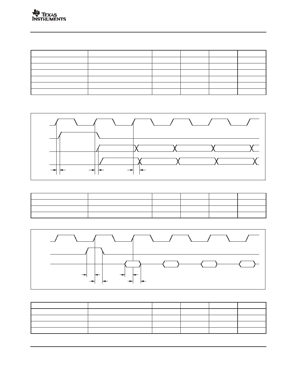
DATA INTERFACE TIMING
DCLK
DFSO
DOUT0
DOUT1
IA[15]
IA[14]
IA[13]
IA[12]
IB[15]
IB[14]
IB[13]
IB[12]
t
d1
t
d2
t
d3
Figure 1. Output Data Interface TIming
PARAMETER
CONDITIONS
MIN
TYP
MAX
UNITS
DCLK to DFSO delay, t
d1
-0.4
3.2
ns
DCLK to DOUT0 delay, t
d2
-0.2
2.5
ns
DCLK to DOUT1 delay, t
d3
-0.2
2.5
ns
DCLK
DFSI
DIN
D[15]
D[14]
D[13]
D[12]
t
su1
t
su2
t
h1
t
h2
Figure 2. Input Data Interface TIming
PARAMETER
CONDITIONS
MIN
TYP
MAX
UNITS
DFSI to DCLK setup time, t
su1
1.2
ns
DFSI to DCLK hold time, t
h1
0.4
ns
DIN to DCLK setup time, t
su2
1.0
ns
DIN to DCLK hold time, t
h2
0.4
ns