 | –≠–ª–µ–∫—Ç—Ä–æ–Ω–Ω—ã–π –∫–æ–º–ø–æ–Ω–µ–Ω—Ç: ALD1000U | –°–∫–∞—á–∞—Ç—å:  PDF PDF  ZIP ZIP |
International Airport Industrial Park ∑ Mailing Address: PO Box 11400, Tucson, AZ 85734 ∑ Street Address: 6730 S. Tucson Blvd., Tucson, AZ 85706 ∑ Tel: (520) 746-1111 ∑ Twx: 910-952-1111
Internet: http://www.burr-brown.com/ ∑ FAXLine: (800) 548-6133 (US/Canada Only) ∑ Cable: BBRCORP ∑ Telex: 066-6491 ∑ FAX: (520) 889-1510 ∑ Immediate Product Info: (800) 548-6132
Precision Programmable
CURRENT/VOLTAGE TRANSMITTER
FEATURES
q
SWITCHABLE OUTPUT
±
10V OR 4-20mA
q
DRIVES 1000
|| 1
µ
F AT 20mA
q
VOLTAGE AND CURRENT SENSE
q
GROUND NOISE SUPPRESSION
q
ERROR DETECTION FLAG
q
OUTPUT DISABLE
q
ACCURACY: 0.05% max
q
WIDE SUPPLY RANGE:
±
11V TO +24/≠15V
Æ
APPLICATIONS
q
PROGRAMMABLE CONTROLLERS
q
STANDARDIZED OUTPUTS FOR
TERMINATION PANELS
q
INDUSTRIAL PROCESS CONTROL
q
PROGRAMMABLE CURRENT SOURCE
q
MOTOR CONTROL SYSTEMS
q
PC AND VME BASED INSTRUMENTATION
q
CONDITIONER FOR STANDARD SENSOR
OUTPUTS
q
TEST EQUIPMENT PIN DRIVER
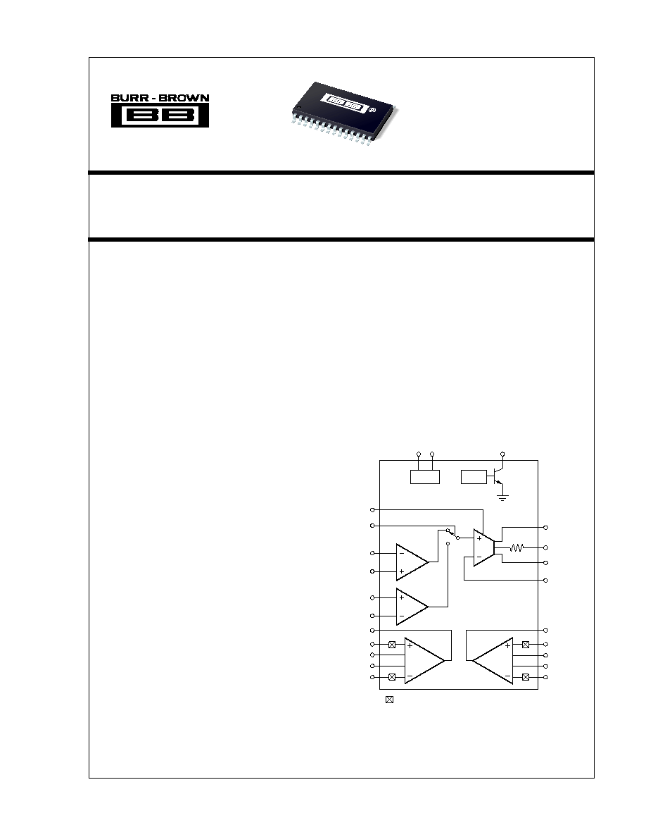
DESCRIPTION
This product is a monolithic programmable voltage-to-
current or voltage-to-voltage analog line driver circuit.
It can convert a
±
10V input into either an output
voltage or current with remote sensing. It provides
drive for external transistors to boost output current to
greater than
±
25mA levels.
Current and voltage sensing can be performed simulta-
neously. Current sensing is achieved through a single
external sense resistor. Voltage sensing is performed
directly across the load. The logic inputs provide for
both output disable and switching between constant
current or constant voltage output functions. An open
collector output provides an error flag for open circuit
loads. The output disable function allows full control
of the output even during power-on and power-off
sequencing. The instrumentation amplifiers are de-
signed to insure that load noise is not circulated within
the control loop.
ALD1000
ALD1000
100
V
Sense
Phase
IA
1
IA
2
Phase Compensation
Voltage Error
Indication
External PNP
Drive
Internal Drive
External NPN
Drive
Open-Loop
Gain Control
IAs Provide
Closed-Loop
Gain Control
IA Gain
Control
V
IN1
V
IN2
Input
Select
Output
Disable
Input Over-Voltage Protection
©
1996 Burr-Brown Corporation
PDS-1292A
Printed in U.S.A. October, 1996
2
Æ
ALD1000
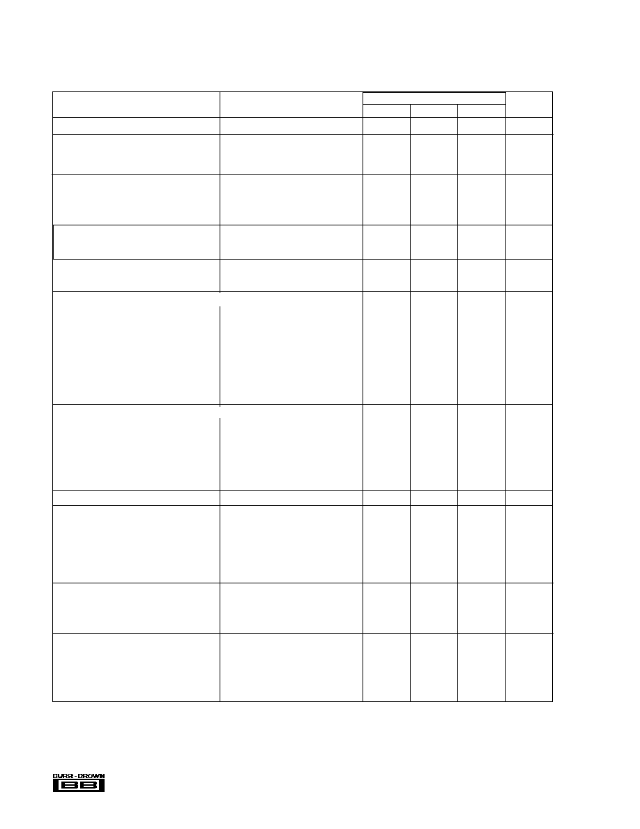
SPECIFICATIONS
At +V
S
= 24V, ≠V
S
= 15V, T
AMB
= 25
∞
C, and 2N2222, 2N2907 external transistors, unless otherwise noted.
ALD1000U
PARAMETER
CONDITIONS
MIN
TYP
MAX
UNITS
TRANSMITTER
SWOP INPUTS
Linear Range Min
Internal Drive Transistors
≠10
V
Linear Range Max
5mA Load
10
V
Input Bias Current
50
pA
XTR OUTPUT
Positive Overvoltage Sense
19.5
V
Negative Overvoltage Sense
Internal Drive Transistors
≠10.5
V
Positive Overcurrent Sense
+25
mA
Negative Overcurrent Sense
≠15
mA
LOGIC INPUTS
Logic Low
0.8
V
Logic High
4.0
2.6
V
LOGIC OUTPUTS
Logic High
5V Logic Supply
4.0
V
Logic Low
with 10k pull-up resistor
0.8
V
OUTPUT--VOLTAGE MODE (Gain = 1 unless otherwise specified)
Span Error
0.5
1
%
Span Drift
50
ppm/
∞
C of FS
Linear Range Min
0.1% of FS
≠10
Linear Range Max
0.1% of FS
10
Output Current Min
Internal Drive Transistors
≠5
mA
Output Current Max
Internal Drive Transistors
5
mA
Short-Circuit Current
Internal Drive Transistors
25
mA
Short-Circuit Current
Internal Drive Transistors
≠15
mA
Non-Linearity
0.005
0.05
%
Initial Offset Voltage--RTI
2
mV
Offset Voltage vs Temperature
20
µ
V/
∞
C
OUTPUT--CURRENT MODE (Gain = 5 with 50
shunt resistor unless otherwise specified)
Span Error
5
%
Span Drift
Gain = 1
(1)
50
ppm/
∞
C of FS
Output Current Min
Internal Drive Transistors
(2)
≠5
mA
Output Current Max
Internal Drive Transistors
(2)
5
mA
Compliance Min
≠10
V
Compliance Max
15
V
Offset Current Min
≠25
µ
A
Offset Current Min
25
µ
A
INSTRUMENTATION AMPLIFIERS R
LOAD
= 10k
IA INPUTS
Linear Input Voltage Min
≠10
V
Linear Input Voltage Max
20
V
Common-Mode Input Voltage Min
V
IN
= 0
≠10
V
Common-Mode Input Voltage Max
V
IN
= 0
20
V
Input Bias Current
100
nA
Initial Offset Voltage
G = 1
≠1
1
mV
CMRR
G = 10
80
100
IA OUTPUTS (with 10k Load)
Output Voltage Max
20
V
Output Voltage Min
≠10
V
+ Short Circuit Current
5
mA
≠ Short Circuit Current
≠12
mA
GAIN EQUATION (gain = 1+50k/R
G
)
Gain Error, G = 1
0.3
%
±
FS
G = 5
0.6
%
±
FS
G = 100
0.8
%
±
FS
Non-Linearity, G = 1
0.004
%
±
FS
G = 5
0.008
%
±
FS
G = 100
0.02
%
±
FS
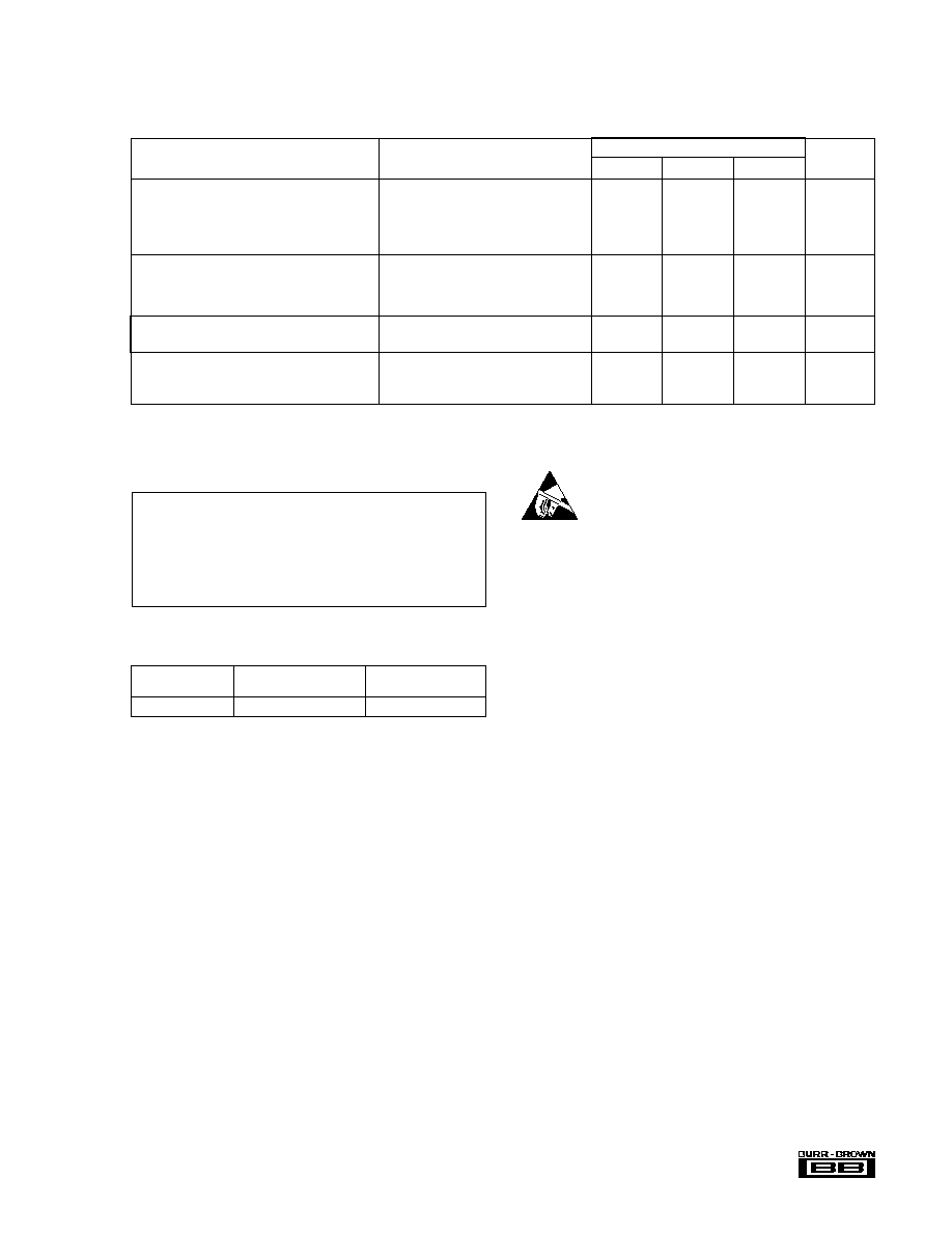
3
Æ
ALD1000
ALD1000U
PARAMETER
CONDITIONS
MIN
TYP
MAX
UNITS
FREQUENCY RESPONSE
G = 1
700
kHz
G = 5
400
kHz
G = 100
50
kHz
Slew Rate
V
O
=
±
10V, G = 10
4
V/
µ
S
SETTLING TIME, 0.01%
G = 1
20
µ
S
G = 5
20
µ
S
G = 100
30
µ
S
POWER SUPPLY
Quiescent Current
Internal Drive Transistors
5
mA
TEMPERATURE RANGE
Operating
≠40
+85
∞
C
Storage
≠65
+150
∞
C
NOTES: (1) Gain drift depends on tempco of 50K factor on gain equation when gain is greater than 1. (2) External Drive capacity varies with configuration. See
Application Note.
ABSOLUTE MAXIMUM RATINGS
Supply Voltage (
±
V
S
) .............................................................. +25V, ≠18V
IA Inputs ............................................................................................
±
40V
SWOP Inputs .......................................................................................
±
V
S
Logic Inputs .................................................................... +V
S
, ≠V
S
+ 0.5V
Junction Temperature ...................................................................... 150
∞
C
Storage Temperature ..................................................... ≠65
∞
C to +150
∞
C
Lead Temperature (soldering, 10s) ............................................... +300
∞
C
Output Short-to-Ground at 25
∞
C ............................................. Continuous
SPECIFICATIONS
(CONT)
At +V
S
= 24V, ≠V
S
= 15V, T
AMB
= 25
∞
C, and 2N2222, 2N2907 external transistors, unless otherwise noted.
The information provided herein is believed to be reliable; however, BURR-BROWN assumes no responsibility for inaccuracies or omissions. BURR-BROWN assumes
no responsibility for the use of this information, and all use of such information shall be entirely at the user's own risk. Prices and specifications are subject to change
without notice. No patent rights or licenses to any of the circuits described herein are implied or granted to any third party. BURR-BROWN does not authorize or warrant
any BURR-BROWN product for use in life support devices and/or systems.
PACKAGE/ORDERING INFORMATION
PACKAGE DRAWING
PRODUCT
PACKAGE
NUMBER
(1)
ALD1000U
28-Pin SOIC
217
NOTE: (1) For detailed drawing and dimension table, please see end of data
sheet, or Appendix C of Burr-Brown IC Data Book.
ELECTROSTATIC
DISCHARGE SENSITIVITY
This integrated circuit can be damaged by ESD. Burr-Brown
recommends that all integrated circuits be handled with ap-
propriate precautions. Failure to observe proper handling and
installation procedures can cause damage.
ESD damage can range from subtle performance degradation
to complete device failure. Precision integrated circuits may
be more susceptible to damage because very small parametric
changes could cause the device not to meet its published
specifications.
4
Æ
ALD1000
PIN ASSIGNMENTS
PIN #
NAME
DESCRIPTION
1
XTR GND
Power ground pin.
2
Disable
A 5V signal puts the internal drive in a high impedance state and limits the external drive capacity.
3
Select
Selects the SWOP amp input. A 5V signal selects inputs N1 and P1.
4
C
C2
C
C1
and C
C2
are for the external compensation capacitor.
5
C
C1
C
C1
and C
C2
are for the external compensation capacitor.
6
P
1
Non-inverting input to the XTR SWOP amp 1.
7
N
1
Inverting input to the XTR SWOP amp 1.
8
A
COM
Signal ground for the instrumentation amplifiers.
9
+V
S
Positive power supply voltage.
10
V
OUT1
Output of the instrumentation amplifier 1.
11
V
INP1
Non-inverting input to instrumentation amplifier 1.
12
R
GB1
Gain set resistor for instrumentation amplifier 1.
13
R
GA1
Gain set resistor for instrumentation amplifier 1.
14
V
INN1
Inverting input of instrumentation amplifier 1.
15
V
INN2
Inverting input of instrumentation amplifier 2.
16
R
GA2
Gain set resistor for instrumentation amplifier 2.
17
R
GB2
Gain set resistor for instrumentation amplifier 2.
18
V
INP2
Non-inverting input to instrumentation amplifier 2.
19
V
OUT2
Output of the instrumentation amplifier 2.
20
≠V
S
Negative power supply voltage.
21
N
2
Inverting input to the XTR SWOP amp 2.
22
P
2
Non-inverting input to the XTR SWOP amp 2.
23
E
Inverting input (emitter) of the output transconductance amplifier.
24
X
P
Base drive for an external, PNP, driver transistor (optional).
25
X
N
Base drive for an external, NPN, driver transistor (optional).
26
C
Output (collector) of the output transconductance amplifier.
27
Bias
Open collector output indicating an internal overcurrent condition.
28
V
ERR
Open collector output indicating an overvoltage condition.
PIN CONFIGURATION
Top View
28-Lead
SOIC
XTR GND
Disable
Select
C
C2
C
C1
P
1
N
1
A
COM
+V
S
V
OUT1
V
INP1
R
GB1
R
GA1
V
INN1
V
ERR
Bias
C
X
N
X
P
E
P
2
N
2
≠V
S
V
OUT2
V
INP2
R
GB2
R
GA2
V
INN2
1
2
3
4
5
6
7
8
9
10
11
12
13
14
28
27
26
25
24
23
22
21
20
19
18
17
16
15
IA IA
TA
5
Æ
ALD1000
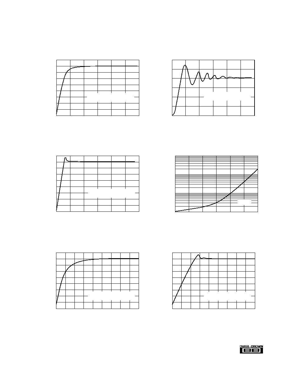
Output (V)
STEP RESPONSE IN VOLTAGE FEEDBACK
Time (
µ
s)
8
6
4
2
0
≠2
≠4
0
100
200
300
400
500
600
Figure 8, R
I
= 400
, C
I
= 100nf
No External Comp Capacitor
5
4
3
2
1
0
≠1
≠2
≠3
≠4
Output (V)
STEP RESPONSE IN THE CURRENT FEEDBACK MODE
0
100
200
300
400
500
600
Time (
µ
s)
Figure 8, R
I
= 400
, C
I
= 100nf
No external comp capacitor
5
4
3
2
1
0
≠1
≠2
≠3
≠4
Output (V)
STEP RESPONSE IN VOLTAGE FEEDBACK
0
100
200
300
400
500
600
Time (
µ
s)
Figure 8, R
I
= 400
, C
I
= 100nf
420pf Compensation Capacitor
5
4
3
2
1
0
≠1
≠2
≠3
≠4
Output (V)
STEP RESPONSE IN CURRENT FEEDBACK MODE
0
500
1000 1500 2000 2500 3000 3500 4000 4500
Time (
µ
s)
Figure 8, R
I
= 400
, C
I
= 1
µ
f
No Comp Capacitor
5
4
3
2
1
0
≠1
≠2
≠3
≠4
Output (V)
STEP RESPONSE LOAD IN THE
VOLTAGE FEEDBACK MODE
0
100
200
300
400
500
600
700
800
900
Time (
µ
s)
Figure 8, R
I
= 400
, C
I
= 1
µ
f
Comp = 2.2nf
Compensation Capacitor
COMPENSATION CAPACITOR vs LOAD CAPACITANCE
1.0E-12
1.0E-11
1.0E-10
1.0E-09
1.0E-08
1.0E-07
1.0E-06
Load Capacitance
1.0E-08
1.0E-09
1.0E-10
1.0E-11
Gain = 1
TYPICAL PERFORMANCE CURVES
At T
A
= +25
∞
C; +V
S
= 24V, ≠V
S
= ≠15V, unless otherwise noted.