 | –≠–ª–µ–∫—Ç—Ä–æ–Ω–Ω—ã–π –∫–æ–º–ø–æ–Ω–µ–Ω—Ç: AMC1210 | –°–∫–∞—á–∞—Ç—å:  PDF PDF  ZIP ZIP |
AMC1210
I
Burr Brown Products
from Texas Instruments
FEATURES
DESCRIPTION
APPLICATIONS
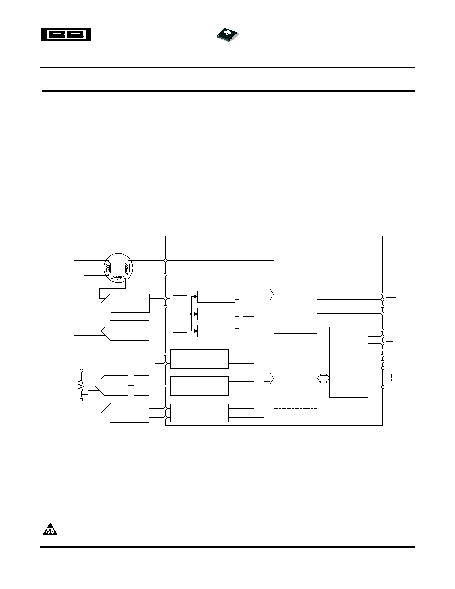
FILTER
MODULE 2
Control Module
Signal
Generator
Interrupt
Unit
Register
Map
Interface
Module
ADS1205
ADS1205
ADS1204
AMC1210
M0
M1
INT
Resolver
ACK
IN1
CLK1
IN3
PWM1
PWM2
CLK
IN2
CLK2
IN4
CLK4
FILTER
MODULE 3
FILTER
MODULE 4
AD0
AD7
ALE
CS
RST
RD
WR
ADS1203
ISO
721
Current
Shunt
Resistor
Input
Control
Sinc Filter/
Integrator
Time Measurement
Comparator
Filter
FILTER MODULE 1
AMC1210
SBAS372A ≠ APRIL 2006 ≠ REVISED OCTOBER 2006
Quad Digital Filter for 2nd-Order Delta-Sigma Modulator
∑
Four Independently-Programmable Digital
The AMC1210 is a four-channel digital filter designed
Filters
specifically for current measurement and resolver
position decoding in motor control applications. Each
∑
Four Window Comparators
input can receive an independent delta-sigma (
)
∑
Three Parallel and One Serial Interface
modulator bit stream. The bit streams are processed
∑
Comprehensive Interrupt System
by four individually-programmable digital decimation
filters. The AMC1210 also offers a flexible interface
∑
Programmable Input Configuration
and
a
comprehensive
interrupt
unit,
allowing
∑
Carrier Frequency Generator for Resolver
customized digital functionality and immediate digital
Applications
threshold comparisons for over-current monitoring.
∑
Current Measurement
∑
Resolver Decoding
Please be aware that an important notice concerning availability, standard warranty, and use in critical applications of Texas
Instruments semiconductor products and disclaimers thereto appears at the end of this data sheet.
All trademarks are the property of their respective owners.
PRODUCTION DATA information is current as of publication date.
Copyright © 2006, Texas Instruments Incorporated
Products conform to specifications per the terms of the Texas
Instruments standard warranty. Production processing does not
necessarily include testing of all parameters.
www.ti.com
ABSOLUTE MAXIMUM RATINGS
DISSIPATION RATINGS
AMC1210
SBAS372A ≠ APRIL 2006 ≠ REVISED OCTOBER 2006
This integrated circuit can be damaged by ESD. Texas Instruments recommends that all integrated circuits be handled with
appropriate precautions. Failure to observe proper handling and installation procedures can cause damage.
ESD damage can range from subtle performance degradation to complete device failure. Precision integrated circuits may be
more susceptible to damage because very small parametric changes could cause the device not to meet its published
specifications.
ORDERING INFORMATION
(1)
SPECIFIED
TRANSPORT
PACKAGE
TEMPERATURE
PACKAGE
ORDERING
MEDIA,
PRODUCT
PACKAGE-LEAD
DESIGNATOR
RANGE
MARKING
NUMBER
QUANTITY
AMC1210IRHAT
Tape and Reel, 250
AMC1210
QFN-40
RHA
≠40∞C to +125∞C
AMC1210I
AMC1210IRHAR
Tape and Reel, 2500
(1)
For the most current specifications and package information, see the Package Option Addendum located at the end of this data sheet or
refer to our web site at
www.ti.com
.
over operating free-air temperature range (unless otherwise noted)
(1)
AMC1210
UNIT
Supply voltage, all supplies (AVDD, BVDD, CVDD, DVDD) to GND
≠0.3 to +6
V
Digital input to GND
GND ≠ 0.3 to BVDD + 0.3
V
Ground voltage difference, AGND to GND
±0.3
V
Input current to any pin except supply
≠10 to +10
mA
Power dissipation
See
Dissipation Ratings Table
Operating virtual junction temperature range, T
J
≠40 to +150
∞C
Operating free-air temperature range, T
A
≠40 to +125
∞C
Storage temperature range, T
STG
≠65 to +150
∞C
Lead temperature, 1,6mm (1/16-inch) from case for 10 seconds
+260
∞C
(1)
Stresses beyond those listed under absolute maximum ratings may cause permanent damage to the device. These are stress ratings
only, and functional operation of the device at these or any other conditions beyond those indicated under the
Electrical Characteristics
is not implied. Exposure to absolute maximum rated conditions for extended periods may affect device reliability.
T
A
+25
∞
C
DERATING FACTOR
T
A
= +70
∞
C
T
A
= +85
∞
C
T
A
= +125
∞
C
PACKAGE
POWER RATING
ABOVE T
A
= +25∞C
POWER RATING
POWER RATING
POWER RATING
RHA
(1)
3787mW
30.3mW/
∞
C
2424mW
1969mW
758mW
(1)
The thermal resistance (junction-to-ambient) of the RHA package is 32
∞
C/W.
2
Submit Documentation Feedback
www.ti.com
ELECTRICAL CHARACTERISTICS
AMC1210
SBAS372A ≠ APRIL 2006 ≠ REVISED OCTOBER 2006
At ≠40∞C to +125∞C, AVDD, CVDD, DVDD = 5V, BVDD = 2.7V, unless otherwise noted. The following condition must be true
on the supplies: CVDD
DVDD
BVDD.
AMC1210
PARAMETER
TEST CONDITIONS
MIN
TYP
MAX
UNIT
DIGITAL INPUT/OUTPUT
Logic levels:
V
OH
BVDD = 2.7
2.4
V
BVDD = 5.0
4.44
V
V
OL
BVDD = 2.7
0.4
V
BVDD = 5.0
0.5
V
System clock frequency
Pin 'CLK'
90
MHz
Pins CLK1, CLK2, CLK3, CLK4
Modulator clock frequency
22
MHz
Mode = 0
SPI interface clock frequency
Pin WR, option 1
25
MHz
SPI interface clock frequency
Pin WR, option 2
40
MHz
Parallel interface read/write frequency
Pin CS
22
MHz
POWER SUPPLY REQUIREMENTS
Power-supply voltage, pin AVDD
4.5
5.5
Power-supply voltage, pins CVDD and DVDD
CVDD
DVDD
BVDD
3.3
5.5
V
Power-supply voltage, pin DVDD
CVDD
DVDD
BVDD
2.7
5.5
V
Total power
(1)
All supplies = 5V
24.5
mW
Power-supply current
One filter module
(2)
260
µ
A/MHz
Power-supply current
Four filter modules
(2)
850
µ
A/MHz
SPI interface
78
µ
A/MHz
Parallel interface
(3)
83
µ
A/MHz
Signal generator
140
µ
A/MHz
SIGNAL GENERATOR OUTPUT
V
OH
R
LOAD
= 50
, bit HPE = 1
4.60
4.73
V
V
OL
R
LOAD
= 50
, bit HPE = 1
0.26
0.4
V
V
OH
R
LOAD
= 500
, bit HPE = 0
4.60
4.73
V
V
OL
R
LOAD
= 500
, bit HPE = 0
0.26
0.4
V
(1)
Power consumption with two filter modules functioning, both set to Sinc
3
, SOSR = 256.
(2)
The filter module is configured with the comparator unit filter set to Sinc
3
, COSR = 32 and the sinc unit filter set to Sinc
3
structure and
SOSR = 256.
(3)
All three modes.
3
Submit Documentation Feedback
www.ti.com
DEVICE INFORMATION
CVDD
IN1
CLK1
IN2
CLK2
IN3
CLK3
IN4
CLK4
AVDD
BVDD
GND
AD0
AD1
AD2
AD3
AD4
AD5
AD6
AD7
1
2
3
4
5
6
7
8
9
10
30
29
28
27
26
25
24
23
22
21
AMC1210
PWM1
GND
11
40
12
39
PWM2
DVDD
AGND
TE
DVDD
RST
GND
M1
CLK
M0
SH1
ALE
SH2
C
S
ACK
RD
INT
WR
13
38
14
37
15
36
16
35
17
34
18
33
19
32
20
31
AMC1210
SBAS372A ≠ APRIL 2006 ≠ REVISED OCTOBER 2006
RHA PACKAGE
QFN-40
(TOP VIEW)
4
Submit Documentation Feedback

www.ti.com
AMC1210
SBAS372A ≠ APRIL 2006 ≠ REVISED OCTOBER 2006
DEVICE INFORMATION (continued)
Table 1. TERMINAL FUNCTIONS
TERMINAL
NO.
NAME
I/O
DESCRIPTION
1
CVDD
Modulator side supply
(1)
2
IN1
Input
Data input from Modulator 1
3
CLK1
Bidirectional
Clock from/to Modulator 1
4
IN2
Input
Data input from Modulator 2
5
CLK2
Bidirectional
Clock from/to Modulator 2
6
IN3
Input
Data input from Modulator 3
7
CLK3
Bidirectional
Clock from/to Modulator 3
8
IN4
Input
Data input from Modulator 4
9
CLK4
Bidirectional
Clock from/to Modulator 4
10
AVDD
Signal generator supply
11
PWM1
Output
Signal generator output
12
PWM2
Output
Signal generator output (inverted)
13
AGND
Signal generator ground
14
DVDD
Core supply
15
GND
Ground
16
CLK
Input
System clock
17
SH1
Input
First asynchronous sample-and-hold
18
SH2
Input
Second asynchronous sample-and-hold
19
ACK
Output
Acknowledge signal
20
INT
Output
Interrupt signal
21
AD7
Bidirectional
Data bus bit 7 (most significant bit)
22
AD6
Bidirectional
Data bus bit 6
23
AD5
Bidirectional
Data bus bit 5
24
AD4
Bidirectional
Data bus bit 4
25
AD3
Bidirectional
Data bus bit 3
26
AD2
Bidirectional
Data bus bit 2
27
AD1
Bidirectional
Data bus bit 1
28
AD0
Bidirectional
Data bus bit 0 (least significant bit)
(2)
29
GND
Ground
30
BVDD
Controller side supply
(3)
31
WR
Input
Write signal
(2)
32
RD
Input
Read signal
(2)
33
CS
Input
Chip select signal
(2)
34
ALE
Input
Address latch enable
(2)
35
M0
Input
First mode pin
36
M1
Input
Second mode pin
37
RST
Input
Active-low asynchronous reset
38
TE
Input
For factory test only; must be tied to ground
39
DVDD
Core supply
40
GND
Ground
(1)
The pins for the modulator side are 1 to 9.
(2)
Functionality is dependent on device setup. To see a list of pin functions/names in each mode, see
Table 3
.
(3)
The pins for the controller side are 16 to 38.
5
Submit Documentation Feedback