 | –≠–ª–µ–∫—Ç—Ä–æ–Ω–Ω—ã–π –∫–æ–º–ø–æ–Ω–µ–Ω—Ç: DAC2902Y | –°–∫–∞—á–∞—Ç—å:  PDF PDF  ZIP ZIP |

Dual, 12-Bit, 125MSPS
DIGITAL-TO-ANALOG CONVERTER
FEATURES
q
q
q
q
q
125MSPS UPDATE RATE
q
q
q
q
q
SINGLE SUPPLY: +3.3V or +5V
q
q
q
q
q
HIGH SFDR: 70dB at f
OUT
= 20MHz
q
q
q
q
q
LOW GLITCH: 2pVs
q
q
q
q
q
LOW POWER: 310mW
q
q
q
q
q
INTERNAL REFERENCE
q
q
q
q
q
POWER-DOWN MODE: 23mW
APPLICATIONS
q
q
q
q
q
COMMUNICATIONS:
Base Stations, WLL, WLAN
Baseband I/Q Modulation
q
q
q
q
q
MEDICAL/TEST INSTRUMENTATION
q
q
q
q
q
ARBITRARY WAVEFORM GENERATORS (ARB)
q
q
q
q
q
DIRECT DIGITAL SYNTHESIS (DDS)
DESCRIPTION
The DAC2902 is a monolithic, 12-bit, dual-channel,
high-speed Digital-to-Analog Converter (DAC), and is opti-
mized to provide high dynamic performance while dissipating
only 310mW.
Operating with high update rates of up to 125MSPS, the
DAC2902 offers exceptional dynamic performance, and
enables the generation of very-high output frequencies suit-
able for "Direct IF" applications. The DAC2902 has been
optimized for communications applications in which sepa-
rate I and Q data are processed while maintaining tight gain
and offset matching.
Each DAC has a high-impedance differential-current output,
suitable for single-ended or differential analog-output con-
figurations.
The DAC2902 combines high dynamic performance with a
high throughput rate to create a cost-effective solution for a
wide variety of waveform-synthesis applications:
∑ Pin compatibility between family members provides 10-bit
(DAC2900), 12-bit (DAC2902), and 14-bit (DAC2904)
resolution.
∑ Pin compatible to the AD9765 dual DAC.
∑ Gain matching is typically 0.5% of full-scale, and offset
matching is specified at 0.02% max.
∑ The DAC2902 utilizes an advanced CMOS process; the
segmented architecture minimizes output-glitch energy,
and maximizes the dynamic performance.
∑ All digital inputs are +3.3V and +5V logic compatible. The
DAC2902 has an internal reference circuit, and allows use
of an external reference.
∑ The DAC2902 is available in a TQFP-48 package, and is
specified over the extended industrial temperature range of
≠40∞C to +85∞C.
DAC2902
DAC2902
SBAS167A ≠ APRIL 2002
www.ti.com
Copyright © 2002, Texas Instruments Incorporated
Please be aware that an important notice concerning availability, standard warranty, and use in critical applications of
Texas Instruments semiconductor products and disclaimers thereto appears at the end of this data sheet.
PRODUCTION DATA information is current as of publication date.
Products conform to specifications per the terms of Texas Instruments
standard warranty. Production processing does not necessarily include
testing of all parameters.

DAC2902
2
SBAS167A
ELECTRICAL CHARACTERISTICS
DAC2902Y
PARAMETER
CONDITIONS
MIN
TYP
MAX
UNITS
RESOLUTION
12
Bits
Output Update Rate (f
CLOCK
)
125
MSPS
STATIC ACCURACY
(1)
Differential Nonlinearity (DNL)
T
A
= +25∞C
≠2.0
±1
+2.0
LSB
T
MIN
to T
MAX
≠2.5
+2.5
LSB
Integral Nonlinearity (INL)
T
A
= +25∞C
≠2.0
±1
+2.0
LSB
T
MIN
to T
MAX
≠3.0
+3.0
LSB
DYNAMIC PERFORMANCE
Spurious-Free Dynamic Range (SFDR)
To Nyquist
f
OUT
= 1MHz, f
CLOCK
= 50MSPS
0dBFS Output
72
82
dBc
≠6dBFS Output
77
dBc
≠12dBFS Output
72
dBc
f
OUT
= 1MHz, f
CLOCK
= 26MSPS
81
dBc
f
OUT
= 2.18MHz, f
CLOCK
= 52MSPS
81
dBc
f
OUT
= 5.24MHz, f
CLOCK
= 52MSPS
81
dBc
f
OUT
= 10.4MHz, f
CLOCK
= 78MSPS
77
dBc
f
OUT
= 15.7MHz, f
CLOCK
= 78MSPS
71
dBc
f
OUT
= 5.04MHz, f
CLOCK
= 100MSPS
80
dBc
f
OUT
= 20.2MHz, f
CLOCK
= 100MSPS
70
dBc
f
OUT
= 20.1MHz, f
CLOCK
= 125MSPS
72
dBc
f
OUT
= 40.2MHz, f
CLOCK
= 125MSPS
64
dBc
Spurious-Free Dynamic Range within a Window
f
OUT
= 1.0MHz, f
CLOCK
= 50MSPS
2MHz Span
80
90
dBc
f
OUT
= 5.02MHz, f
CLOCK
= 50MSPS
10MHz Span
88
dBc
f
OUT
= 5.03MHz, f
CLOCK
= 78MSPS
10MHz Span
88
dBc
f
OUT
= 5.04MHz, f
CLOCK
= 125MSPS
10MHz Span
88
dBc
Total Harmonic Distortion (THD)
f
OUT
= 1MHz, f
CLOCK
= 50MSPS
≠79
≠70
dBc
f
OUT
= 5.02MHz, f
CLOCK
= 50MSPS
≠77
dBc
f
OUT
= 5.03MHz, f
CLOCK
= 78MSPS
≠76
dBc
f
OUT
= 5.04MHz, f
CLOCK
= 125MSPS
≠75
dBc
Multitone Power Ratio
8 Tone with 110kHz Spacing
f
OUT
= 2.0MHz to 2.99MHz, f
CLOCK
= 65MSPS
0dBFS Output
80
dBc
T
MIN
to T
MAX
, +V
A
= +5V, +V
D
= +3.3V, differential transformer coupled output, 50˝ doubly-terminated, unless otherwise noted. Independant Gain Mode.
ELECTROSTATIC
DISCHARGE SENSITIVITY
This integrated circuit can be damaged by ESD. Texas Instru-
ments recommends that all integrated circuits be handled with
appropriate precautions. Failure to observe proper handling
and installation procedures can cause damage.
ESD damage can range from subtle performance degradation
to complete device failure. Precision integrated circuits may
be more susceptible to damage because very small parametric
changes could cause the device not to meet its published
specifications.
ABSOLUTE MAXIMUM RATINGS
+V
A
to AGND ........................................................................ ≠0.3V to +6V
+V
D
to DGND ........................................................................ ≠0.3V to +6V
AGND
to DGND ................................................................. ≠0.3V to ≠0.3V
+V
A
to +V
D
............................................................................... ≠6V to +6V
CLK, PD, WRT to DGND ........................................... ≠0.3V to V
D
+ 0.3V
D0-D11 to DGND ....................................................... ≠0.3V to V
D
+ 0.3V
I
OUT
, I
OUT
to AGND ........................................................ ≠1V to V
A
+ 0.3V
GSET to AGND .......................................................... ≠0.3V to V
A
+ 0.3V
REF
IN
, FSA to AGND ................................................. ≠0.3V to V
A
+ 0.3V
Junction Temperature .................................................................... +150∞C
Case Temperature ......................................................................... +100∞C
Storage Temperature .................................................................... +125∞C
PACKAGE
SPECIFIED
DRAWING
PACKAGE
TEMPERATURE
PACKAGE
ORDERING
TRANSPORT
PRODUCT
PACKAGE
NUMBER
DESIGNATOR
RANGE
MARKING
NUMBER
(1)
MEDIA
DAC2902Y
TQFP-48
355
48 PDF
≠40∞C to +85∞C
DAC2902Y
DAC2902Y/250
Tape and Reel
"
"
"
"
"
"
DAC2902Y/2K
Tape and Reel
NOTE: (1) Models with a slash (/) are available only in Tape and Reel in the quantities indicated (e.g., /2K indicates 2000 devices per reel). Ordering 2000 pieces
of "DAC2902Y/2K" will get a single 2000-piece Tape and Reel.
PACKAGE/ORDERING INFORMATION
PRODUCT
EVM ORDERING NUMBER
COMMENT
DAC2902
DAC2902-EVM
Fully populated evaluation board. See user manual for details.

DAC2902
3
SBAS167A
ELECTRICAL CHARACTERISTICS
(Cont.)
T
MIN
to T
MAX
, +V
A
= +5V, +V
D
= +3.3V, differential transformer coupled output, 50˝ doubly terminated, unless otherwise noted. Independant Gain Mode.
DYNAMIC PERFORMANCE (Cont.)
Signal-to-Noise Ratio (SNR)
0dBFS Output
68
dBc
f
OUT
= 5.02MHz, f
CLOCK
= 50MHz
Signal-to-Noise and Distortion (SINAD)
0dBFS Output
67
dBc
f
OUT
= 5.02MHz, f
CLOCK
= 50MHz
Channel Isolation
f
OUT
= 1MHz, f
CLOCK
= 52MSPS
85
dBc
f
OUT
= 20MHz, f
CLOCK
= 125MSPS
77
dBc
Output Settling Time
(2)
to 0.1%
30
ns
Output Rise Time
(2)
10% to 90%
2
ns
Output Fall Time
(2)
10% to 90%
2
ns
Glitch Impulse
2
pV-s
DC ACCURACY
Full-Scale Output Range
(3)
(FSR)
All Bits HIGH, I
OUT
2
20
mA
Output Compliance Range
≠1.0
+1.25
V
Gain Error--Full-Scale
With Internal Reference
≠5
±1
+5
%FSR
Gain Error
With External Reference
≠2.5
±1
+2.5
%FSR
Gain Matching
With Internal Reference
≠2.0
0.5
+2.0
%FSR
Gain Drift
With Internal Reference
±50
ppmFSR/∞C
Offset Error
With Internal Reference
≠0.02
+0.02
%FSR
Offset Drift
With Internal Reference
±0.2
ppmFSR/∞C
Power-Supply Rejection, +V
A
+5V, ±10%
≠0.2
+0.2
%FSR/V
Power-Supply Rejection, +V
D
+3.3V, ±10%
≠0.025
+0.025
%FSR/V
Output Noise
I
OUT
= 20mA, R
LOAD
= 50
50
pA/
Hz
I
OUT
= 2mA
30
pA/sHz
Output Resistance
200
k
Output Capacitance
I
OUT
, I
OUT
to Ground
6
pF
REFERENCE/CONTROL AMP
Reference Voltage
+1.18
+1.25
+1.31
V
Reference Voltage Drift
±50
ppmFSR/∞C
Reference Output Current
100
nA
Reference Multiplying Bandwidth
0.3
MHz
Input Compliance Range
+0.5
+1.25
V
DIGITAL INPUTS
Logic Coding
Straight Binary
Logic High Voltage, V
IH
+V
D
= +5V
3.5
5
V
Logic Low Voltage, V
IL
+V
D
= +5V
0
1.2
V
Logic High Voltage, V
IH
+V
D
= 3.3V
2
3
V
Logic Low Voltage, V
IL
+V
D
= 3.3V
0
0.8
V
Logic High Current
,
I
IH
(4)
+V
D
= 3.3V
±10
µA
Logic Low Current
+V
D
= 3.3V
±10
µA
Input Capacitance
5
pF
POWER SUPPLY
Supply Voltages
+V
A
+3.0
+5
+5.5
V
+V
D
+3.0
+3.3
+5.5
V
Supply Current
I
VA
(5)
V
A
= +5V, l
OUT
= 20mA
59
64
mA
I
VA
(5)
Power-Down Mode
1.7
3
mA
I
VD
(5)
4.2
7
mA
I
VD
(6)
15.5
18
mA
Power Dissipation
(5)
V
A
= +5V, V
D
= 3.3V, l
OUT
= 20mA
310
345
mW
Power Dissipation
(6)
V
A
= +5V, V
D
= 3.3V, l
OUT
= 20mA
345
380
mW
Power Dissipation
(5)
V
A
= +5V, V
D
= 3.3V, l
OUT
= 2mA
130
mW
Power Dissipation
Power-Down Mode
23
38
mW
Thermal Resistance, TQFP-48
JA
60
∞C/W
JC
13
∞C/W
TEMPERATURE RANGE
Specified
Ambient
≠40
+85
∞C
Operating
Ambient
≠40
+85
∞C
NOTES: (1) At output l
OUT
, while driving a virtual ground. (2) Measured single-ended into 50˝ load. (3) Nominal full-scale output current is 32 ∑ I
REF
; see Application
section for details. (4) Typically 45µA for the PD pin, which has an internal pull-down resistor. (5) Measured at f
CLOCK
= 25MSPS and f
OUT
= 1MHz. (6) Measured
at f
CLOCK
= 100MSPS and f
OUT
= 40MHz.
DAC2902Y
PARAMETER
CONDITIONS
MIN
TYP
MAX
UNITS
DAC2902
4
SBAS167A
PIN
DESIGNATOR
DESCRIPTION
1-12
D[11:0]_1
Data Port DAC1, Data Bit 11 (MSB) to Bit 0 (LSB).
13, 14
NC
No Connection
15
DGND
Digital Ground
16
+V
D
Digital Supply, +3.0V to +5.5V
17
WRT1
DAC1 Input Latches Write Signal
18
CLK1
Clock Input DAC1
19
CLK2
Clock Input DAC2
20
WRT2
DAC2 Input Latches Write Signal
21
DGND
Digital Ground
22
+V
D
Digital Supply, +3.0V to +5.5V
23-34
D[11:0]_2
Data Port DAC2, Data Bit 11 (MSB) to Bit 0 (LSB).
35, 36
NC
No Connection
37
PD
Power-Down Function Control Input; "H" = DAC in power-down mode; "L" = DAC in normal operation (Internal pull-down for default "L").
38
AGND
Analog Ground
39
I
OUT
2
Current Output DAC2. Full-scale with all bits of data port 2 HIGH.
40
I
OUT
2
Complementary Current Output DAC2. Full-scale with all bits of data port 2 LOW.
41
FSA2
Full-Scale Adjust, DAC2. Connect External R
SET
Resistor
42
GSET
Gain-Setting Mode (H = 1 Resistor, L = 2 Resistor)
43
REF
IN
Internal Reference Voltage output; External Reference Voltage input. Bypass with 0.1µF to AGND for internal reference
operation.
44
FSA1
Full-Scale Adjust, DAC1. Connect External R
SET
Resistor
45
I
OUT
1
Complementary Current Output DAC1. Full-scale with all bits of data port 1 LOW.
46
I
OUT
1
Current Output DAC1. Full-scale with all bits of data port 1 HIGH.
47
+V
A
Analog Supply, +3.0V to +5.5V
48
NC
No Connection
PIN DESCRIPTIONS
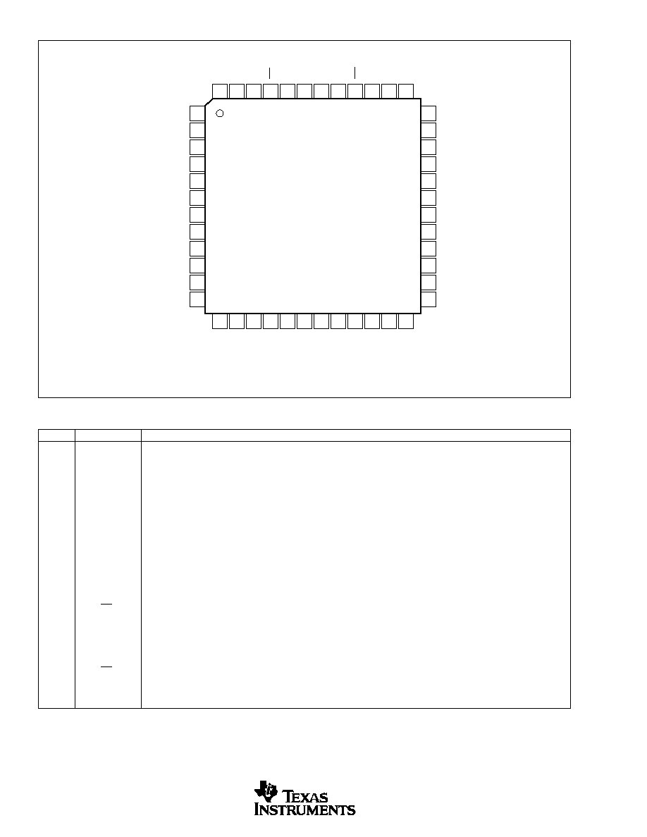
PIN CONFIGURATION
Top View
TQFP-48
36
35
34
33
32
31
30
29
28
27
26
25
1
2
3
4
5
6
7
8
9
10
11
12
48
47
46
45
44
43
42
41
40
39
38
13
14
15
16
17
18
19
20
21
22
23
37
24
DAC2902
NC
NC
D0_2
D1_2
D2_2
D3_2
D4_2
D5_2
D6_2
D7_2
D8_2
D9_2
NC
+V
A
I
OUT
1
I
OUT
1
FSA
REF
IN
GSET
FSA2
I
OUT
2
I
OUT
2
AGND
PD
NC
NC
DGND
+V
D
WRT1
CLK1
CLK2
WRT2
DGND
+V
D
D11_2 (MSB)
D10_2
D11_1 (MSB)
D10_1
D9_1
D8_1
D7_1
D6_1
D5_1
D4_1
D3_1
D2_1
D1_1
D0_1

DAC2902
5
SBAS167A
SYMBOL
DESCRIPTION
MIN
TYP
MAX
UNITS
t
S
Input Setup Time
2
ns
t
H
Input Hold Time
1.5
ns
t
LPW,
t
CPW
Latch/Clock Pulsewidth
3.5
4
ns
t
CW
Delay Rising CLK Edge to
0
t
PW
≠ 2
ns
Rising WRT Edge
t
PD
Propagation Delay
1
ns
t
SET
Settling Time (0.1%)
30
ns
TIMING DIAGRAM
t
PD
t
H
t
LPW
t
CPW
t
CW
t
SET
D[11:0]
(n)
D[11:0]
(n + 1)
t
S
I
OUT(n)
I
OUT(n +1)
50%
DATA IN
WRT1
WRT2
CLK1
CLK2
I
OUT
1
I
OUT
2
DIGITAL INPUTS AND TIMING
The data input ports of the DAC2902 accepts a standard
positive coding with data bit D11 being the most significant
bit (MSB). The converter outputs support a clock rate of up
to 125MSPS. The best performance will typically be achieved
with a symmetric duty cycle for write and clock; however,
the duty cycle may vary as long as the timing specifications
are met. Also, the set-up and hold times may be chosen
within their specified limits.
All digital inputs of the DAC2902 are CMOS compatible.
The logic thresholds depend on the applied digital supply
voltages, such that they are set to approximately half the
supply voltage; V
th
= +V
D
/2 (±20% tolerance). The DAC2902
is designed to operate with a digital supply (+V
D
) of +3.0V
to +5.5V.
The two converter channels within the DAC2902 consist of
two independent, 12-bit, parallel data ports. Each DAC-
channel is controlled by its own set of write (WRT1, WRT2)
and clock (CLK1, CLK2) inputs. Here, the WRT lines
control the channel input latches and the CLK lines control
the DAC latches. The data is first loaded into the input latch
by a rising edge of the WRT line. This data is presented to
the DAC latch on the following falling edge of the WRT
signal. On the next rising edge of the CLK line, the DAC is
updated with the new data and the analog output signal will
change accordingly. The double latch architecture of the
DAC2902 results in a defined sequence for the WRT and
CLK signals, expressed by parameter `t
CW
'. A correct tim-
ing is observed when the rising edge of CLK occurs at the
same time, or before, the rising edge of the WRT signal. This
condition can simply be met by connecting the WRT and
CLK lines together. Note that all specifications were mea-
sured with the WRT and CLK lines connected together.

DAC2902
6
SBAS167A
TYPICAL CHARACTERISTICS
T
A
= 25∞C, +V
D
= +3.3V, +V
A
= +5V, differential transformer coupled, I
OUT
= 20mA, 50˝ double terminated load, SFDR up to Nyquist, unless otherwise noted.
SFDR vs f
OUT
AT 26MSPS
f
OUT
(MHz)
SFDR (dBc)
90
85
80
75
70
65
60
4
2
6
8
10
12
0
0dBFS
≠6dBFS
SFDR vs f
OUT
AT 52MSPS
f
OUT
(MHz)
SFDR (dBc)
90
85
80
75
70
65
60
10
5
15
20
25
0
0dBFS
≠6dBFS
SFDR vs f
OUT
AT 78MSPS
f
OUT
(MHz)
SFDR (dBc)
85
80
75
70
65
60
55
10
5
15
20
25
30
35
0
0dBFS
≠6dBFS
SFDR vs f
OUT
AT 100MSPS
f
OUT
(MHz)
SFDR (dBc)
85
80
75
70
65
60
55
50
10
5
15
20
25
30
35
40
45
0
0dBFS
≠6dBFS
TYPICAL DNL
Code
DNL (LSBs)
1.4
1.2
1
0.8
0.6
0.4
0.2
0
≠0.2
≠0.4
≠0.6
≠0.8
≠1
1k
500
1k5
2k
2k5
3k
3k5
4k
0
TYPICAL INL
Code
INL (LSBs)
1.5
1
0.5
0
≠0.5
≠1
≠1.5
1k
500
1k5
2k
2k5
3k
3k5
4k
0

DAC2902
7
SBAS167A
SFDR vs f
OUT
AT 125MHz
f
OUT
(MHz)
SFDR (dBc)
85
80
75
70
65
60
55
50
20
10
30
40
50
60
0
≠6dBFS
0dBFS
SFDR AT 125MSPS vs TEMPERATURE
Temperature (
∞
C)
SFDR (dBc)
90
85
80
75
70
65
60
55
50
0
≠20
25
50
70
85
≠40
2MHz
40MHz
10MHz
20MHz
SINAD vs f
CLK
AND I
OUT
AT 5MHz
f
CLK
(MSPS)
SINAD (dBc)
70
67.5
65
62.5
60
40
60
80
100
120
140
20
20mA
10mA
5mA
GAIN AND OFFSET DRIFT
Temperature (
∞
C)
Gain Error (% FS)
0.8
0.6
0.4
0.2
0
≠0.2
≠0.4
≠0.6
≠0.8
Offset Error (% FS)
0.004
0.003
0.002
0.001
0
≠0.001
≠0.002
≠0.003
≠0.004
0
≠20
20
40
60
80
85
≠40
Offset Error
Gain Error
SFDR vs I
OUT
FS AND f
OUT
AT 78MSPS, 0dBFS
f
OUT
(MHz)
SFDR (dBc)
80
78
76
74
72
70
68
66
64
62
60
10
5
15
20
25
0
I
OUT
FS = 20mA
I
OUT
FS = 10mA
I
OUT
FS = 2mA
I
OUT
FS = 5mA
I
VD
vs RATIO AT +V
D
= +3.3V
Ratio (F
OUT
/F
CLK
)
I
VD
(mA)
25
20
15
10
5
0
0.10
0.05
0.15
0.20
0.25
0.30
0.35
0.40
0.45
0.00
125MSPS
100MSPS
78MSPS
52MSPS
26MSPS
TYPICAL CHARACTERISTICS
(Cont.)
T
A
= 25∞C, +V
D
= +3.3V, +V
A
= +5V, differential transformer coupled, I
OUT
= 20mA, 50˝ double terminated load, SFDR up to Nyquist, unless otherwise noted.

DAC2902
8
SBAS167A
TYPICAL CHARACTERISTICS
(Cont.)
T
A
= 25∞C, +V
D
= +3.3V, +V
A
= +5V, differential transformer coupled, I
OUT
= 20mA, 50˝ double terminated load, SFDR up to Nyquist, unless otherwise noted.
I
VA
vs I
OUT
FS
I
OUT
FS (mA)
I
VA
(mA)
60
55
50
45
40
35
30
25
20
15
10
10
5
15
20
25
0
SINGLE-TONE SFDR
Frequency (MHz)
Magnitude (dBm)
10
0
≠10
≠20
≠30
≠40
≠50
≠60
≠70
≠80
≠90
4
8
12
16
20
0
f
CLOCK
= 52MSPS
f
OUT
= 5.23MHz
Amplitude = 0dBFS
SINGLE-TONE SFDR
Frequency (MHz)
Magnitude (dBm)
10
0
≠10
≠20
≠30
≠40
≠50
≠60
≠70
≠80
≠90
10
20
30
40
50
0
f
CLOCK
= 100MSPS
f
OUT
= 20.2MHz
Amplitude = 0dBFS
DUAL-TONE SFDR
Frequency (MHz)
Magnitude (dBm)
10
0
≠10
≠20
≠30
≠40
≠50
≠60
≠70
≠80
≠90
7.8
15.6
23.4
31.2
39.0
0
f
CLOCK
= 78MSPS
f
OUT
1 = 9.44MHz
f
OUT
2 = 10.44MHz
Amplitude = 0dBFS
FOUR-TONE SFDR
Frequency (MHz)
Magnitude (dBm)
10
0
≠10
≠20
≠30
≠40
≠50
≠60
≠70
≠80
≠90
5
10
15
20
25
0
f
CLOCK
= 50MSPS
f
OUT
1 = 6.25MHz
f
OUT
2 = 6.75MHz
f
OUT
3 = 7.25MHz
f
OUT
4 = 7.75MHz
Amplitude = 0dBFS

DAC2902
9
SBAS167A
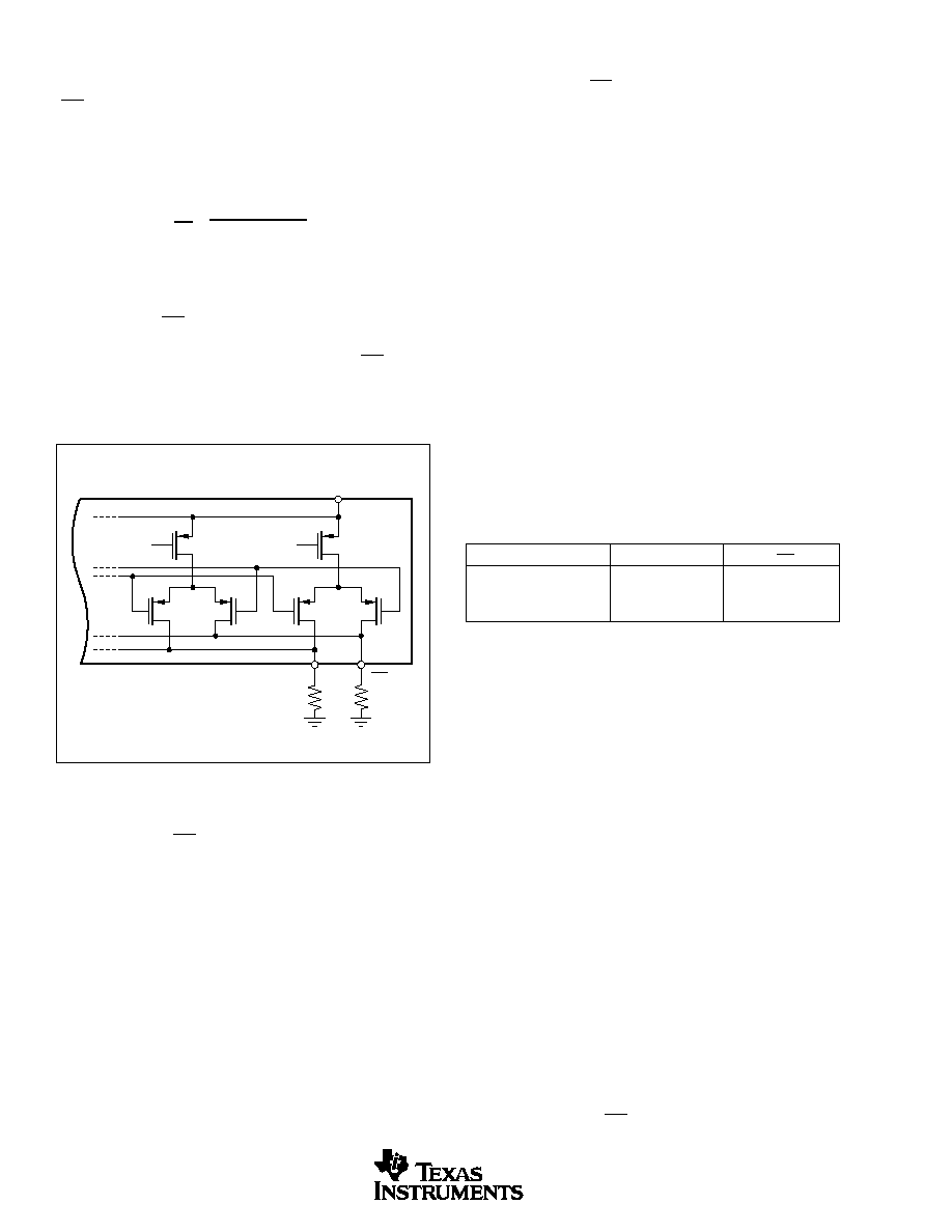
FIGURE 1. Block Diagram of the DAC2902.
APPLICATION INFORMATION
THEORY OF OPERATION
The architecture of the DAC2902 uses the current steering
technique to enable fast switching and a high update rate.
The core element within the monolithic DAC is an array of
segmented current sources that are designed to deliver a full-
scale output current of up to 20mA, as shown in Figure 1. An
internal decoder addresses the differential current switches
each time the DAC is updated and a corresponding output
current is formed by steering all currents to either output
summing node, I
OUT
or I
OUT
. The complementary outputs
deliver a differential output signal, which improves the
dynamic performance through reduction of even-order har-
monics, common-mode signals (noise), and double the peak-
to-peak output signal swing by a factor of two, compared to
single-ended operation.
The segmented architecture results in a significant reduction
of the glitch energy, improves the dynamic performance
(SFDR), and DNL. The current outputs maintain a very high
output impedance of greater than 200k˝.
The full-scale output current is determined by the ratio of the
internal reference voltage (approx. +1.25V) and an external
resistor, R
SET
. The resulting I
REF
is internally multiplied by a
factor of 32 to produce an effective DAC output current that
can range from 2mA to 20mA, depending on the value of R
SET
.
The DAC2902 is split into a digital and an analog portion,
each of which is powered through its own supply pin. The
digital section includes edge-triggered input latches and the
decoder logic, while the analog section comprises the cur-
rent source array with its associated switches, and the
reference circuitry.
DAC TRANSFER FUNCTION
Each of the DACs in the DAC2902 has a complementary
current output, I
OUT
1 and I
OUT
2. The full-scale output cur-
rent, I
OUTFS
, is the summation of the two complementary
output currents:
I
OUTFS
= I
OUT
+ I
OUT
(1)
The individual output currents depend on the DAC code and
can be expressed as:
I
OUT
= I
OUTFS
∑ (Code/4096)
(2)
I
OUT
= I
OUTFS
∑ (4095 - Code)
(3)
where `Code' is the decimal representation of the DAC data
input word. Additionally, I
OUTFS
is a function of the refer-
ence current I
REF
, which is determined by the reference
voltage and the external setting resistor, R
SET
.
I
OUTFS
= 32 ∑ I
REF
= 32 ∑ V
REF
/R
SET
(4)
In most cases the complementary outputs will drive resistive
loads or a terminated transformer. A signal voltage will
develop at each output according to:
V
OUT
= I
OUT
∑ R
LOAD
(5)
V
OUT
= I
OUT
∑ R
LOAD
(6)
DAC
Latch 1
WRT1
CLK1
CLK2
WRT2
Data Input
Port 2
D[11:0]_2
Data Input
Port 1
D[11:0]_1
l
OUT
1
l
OUT
1
Input
Latch 1
Reference
Control Amplifier
FSA2
REF
IN
FSA1
GSET
PD
DAC1
Segmented Switches
Current Sources
DAC2902
l
OUT
2
l
OUT
2
+V
A
+V
D
+V
D
DAC
Latch 2
Input
Latch 2
DAC2
Segmented Switches
Current Sources
AGND
DGND
DGND
DAC2902
10
SBAS167A
The value of the load resistance is limited by the output
compliance specification of the DAC2902. To maintain
specified linearity performance, the voltage for I
OUT
and
I
OUT
should not exceed the maximum allowable compliance
range.
The two single-ended output voltages can be combined to
find the total differential output swing:
V
OUTDIFF
=
V
OUT
≠ V
OUT
=
(2
∑
Code≠ 4095)
4096
∑
I
OUTFS
∑
R
LOAD
(7)
ANALOG OUTPUTS
The DAC2902 provides two complementary current out-
puts, I
OUT
and I
OUT
. The simplified circuit of the analog
output stage representing the differential topology is shown
in Figure 2. The output impedance of I
OUT
and I
OUT
results
from the parallel combination of the differential switches,
along with the current sources and associated parasitic
capacitances.
be adapted to the output of the DAC2902 by selecting a
suitable transformer while maintaining optimum voltage
levels at I
OUT
and I
OUT
. Furthermore, using the differential
output configuration in combination with a transformer will
be instrumental for achieving excellent distortion perfor-
mance. Common-mode errors, such as even-order harmon-
ics or noise, can be substantially reduced. This is particularly
the case with high output frequencies.
For those applications requiring the optimum distortion and
noise performance, it is recommended to select a full-scale
output of 20mA. A lower full-scale range down to 2mA may
be considered for applications that require a low power
consumption, but can tolerate a slightly reduced perfor-
mance level.
OUTPUT CONFIGURATIONS
The current outputs of the DAC2902 allow for a variety of
configurations, some of which are illustrated in Table I. As
mentioned previously, utilizing the converter's differential
outputs will yield the best dynamic performance. Such a
differential output circuit may consist of an RF transformer
or a differential amplifier configuration. The transformer
configuration is ideal for most applications with ac coupling,
while op amps will be suitable for a DC-coupled configura-
tion.
The signal voltage swing that may develop at the two
outputs, I
OUT
and I
OUT
, is limited by a negative and positive
compliance. The negative limit of ≠1V is given by the
breakdown voltage of the CMOS process, and exceeding it
will compromise the reliability of the DAC2902, or even
cause permanent damage. With the full-scale output set to
20mA, the positive compliance equals 1.25V, operating with
an analog supply of +V
A
= 5V. Note that the compliance
range decreases to about 1V for a selected output current of
I
OUTFS
= 2mA. Care should be taken that the configuration
of DAC2902 does not exceed the compliance range to avoid
degradation of the distortion performance and integral lin-
earity.
Best distortion performance is typically achieved with the
maximum full-scale output signal limited to approximately
0.5Vp-p. This is the case for a 50
doubly-terminated load
and a 20mA full-scale output current. A variety of loads can
The single-ended configuration may be considered for appli-
cations requiring a unipolar output voltage. Connecting a
resistor from either one of the outputs to ground will convert
the output current into a ground-referenced voltage signal.
To improve on the DC linearity by maintaining a virtual
ground, an I-to-V or op-amp configuration may be consid-
ered.
DIFFERENTIAL WITH TRANSFORMER
Using an RF transformer provides a convenient way of convert-
ing the differential output signal into a single-ended signal
while achieving excellent dynamic performance (see Figure 3).
The appropriate transformer should be carefully selected based
on the output frequency spectrum and impedance requirements.
The differential transformer configuration has the benefit of
significantly reducing common-mode signals, thus improving
the dynamic performance over a wide range of frequencies.
Furthermore, by selecting a suitable impedance ratio (winding
ratio), the transformer can be used to provide optimum imped-
ance matching while controlling the compliance voltage for the
converter outputs. The model shown, ADTT1-1 (by Mini-
Circuits), has a 1:1 ratio and may be used to interface the
DAC2902 to a 50
load. This results in a 25
load for each of
the outputs, I
OUT
and I
OUT
. The output signals are ac coupled
and inherently isolated because of its magnetic coupling.
FIGURE 2. Equivalent Analog Output.
I
OUT
I
OUT
DAC2902
R
L
R
L
+V
A
INPUT CODE (D11 - D0)
I
OUT
I
OUT
1111 1111 1111
20mA
0mA
1000 0000 0000
10mA
10mA
0000 0000 0000
0mA
20mA
TABLE I. Input Coding Versus Analog Output Current.

DAC2902
11
SBAS167A
As shown in Figure 3, the transformer's center tap is con-
nected to ground. This forces the voltage swing on I
OUT
and
I
OUT
to be centered at 0V. In this case the two resistors, R
L
,
may be replaced with one, R
DIFF
, or omitted altogether. This
approach should only be used if all components are close to
each other, and if the VSWR is not important. A complete
power transfer from the DAC output to the load can be
realized, but the output compliance range should be ob-
served. Alternatively, if the center tap is not connected, the
signal swing will be centered at R
L
∑ I
OUTFS
/2. However, in
this case, the two resistors (R
L
) must be used to enable the
necessary DC-current flow for both outputs.
The OPA680 is configured for a gain of two. Therefore,
operating the DAC2902 with a 20mA full-scale output will
produce a voltage output of ±1V. This requires the amplifier
to operate off of a dual power supply (±5V). The tolerance
of the resistors typically sets the limit for the achievable
common-mode rejection. An improvement can be obtained
by fine tuning resistor R
4
.
This configuration typically delivers a lower level of ac
performance than the previously discussed transformer solu-
tion because the amplifier introduces another source of dis-
tortion. Suitable amplifiers should be selected based on their
slew-rate, harmonic distortion, and output swing capabilities.
High-speed amplifiers like the OPA680 or OPA687 may be
considered. The ac performance of this circuit may be im-
proved by adding a small capacitor (C
DIFF
) between the
outputs I
OUT
and I
OUT
, as shown in Figure 4). This will
introduce a real pole to create a low-pass filter in order to
slew-limit the DAC's fast output signal steps, that otherwise
could drive the amplifier into slew-limitations or into an
overload condition; both would cause excessive distortion.
The difference amplifier can easily be modified to add a level
shift for applications requiring the single-ended output volt-
age to be unipolar, i.e., swing between 0V and +2V.
DUAL TRANSIMPEDANCE OUTPUT CONFIGURATION
The circuit example of Figure 5 shows the signal output
currents connected into the summing junctions of the dual
voltage-feedback op amp OPA2680 that is set up as a
transimpedance stage, or `I-to-V converter'. With this cir-
cuit, the DAC's output will be kept at a virtual ground,
minimizing the effects of output impedance variations, which
results in the best DC linearity (INL). As mentioned previ-
ously, care should be taken not to drive the amplifier into
slew-rate limitations, and produce unwanted distortion.
DIFFERENTIAL CONFIGURATION USING AN OP AMP
If the application requires a DC-coupled output, a difference
amplifier may be considered, as shown in Figure 4. Four
external resistors are needed to configure the voltage-feed-
back op amp OPA680 as a difference amplifier performing
the differential to single-ended conversion. Under the shown
configuration, the DAC2902 generates a differential output
signal of 0.5Vp-p at the load resistors, R
L
. The resistor
values shown were selected to result in a symmetric 25
loading for each of the current outputs since the input
impedance of the difference amplifier is in parallel to resis-
tors R
L
, and should be considered.
FIGURE 4. Difference Amplifier Provides Differential to
Single-Ended Conversion and DC-Coupling.
FIGURE 5. Dual, Voltage-Feedback Amplifier OPA2680
Forms Differential Transimpedance Amplifier.
FIGURE 3. Differential Output Configuration Using an RF
Transformer.
DAC2902
I
OUT
I
OUT
1:1
ADTT1-1
(Mini-Circuits)
R
L
50
R
L
50
R
S
50
R
DIFF
100
I
OUT
I
OUT
DAC2902
R
L
26.1
R
L
28.7
R
4
402
R
3
200
R
2
402
R
1
200
OPA680
C
OPT
+5V
V
OUT
≠5V
1/2
OPA2680
1/2
OPA2680
DAC2902
≠V
OUT
= I
OUT
∑ R
F
1
≠V
OUT
= I
OUT
∑ R
F
2
R
F1
R
F2
C
F1
C
F2
C
D1
C
D2
I
OUT
I
OUT
50
50
≠5V
+5V
DAC2902
12
SBAS167A
The DC gain for this circuit is equal to feedback resistor R
F
.
At high frequencies, the DAC output impedance (C
D1
, C
D2
)
will produce a 0 in the noise gain for the OPA2680 that may
cause peaking in the closed-loop frequency response. C
F
is
added across R
F
to compensate for this noise gain peaking.
To achieve a flat transimpedance frequency response, the
pole in each feedback network should be set to:
1
2
R
F
C
F
=
GBP
4
R
F
C
D
(8)
with GBP = Gain Bandwidth Product of OPA,
which will give a corner frequency f
-3dB
of approximately:
f
-
3dB
=
GBP
2
R
F
C
D
(9)
The full-scale output voltage is simply defined by the prod-
uct of I
OUTFS
∑ R
F
, and has a negative unipolar excursion. To
improve on the ac performance of this circuit, adjustment of
R
F
and/or I
OUTFS
should be considered. Further extensions of
this application example may include adding a differential
filter at the OPA2680's output followed by a transformer, in
order to convert to a single-ended signal.
SINGLE-ENDED CONFIGURATION
Using a single-load resistor connected to the one of the DAC
outputs, a simple current-to-voltage conversion can be ac-
complished. The circuit in Figure 6 shows a 50
resistor
connected to I
OUT
, providing the termination of the further
connected 50
cable. Therefore, with a nominal output
current of 20mA, the DAC produces a total signal swing of
0V to 0.5V into the 25
load.
Different load resistor values may be selected as long as the
output compliance range is not exceeded. Additionally, the
output current, I
OUTFS
, and the load resistor, may be mutu-
ally adjusted to provide the desired output signal swing and
performance.
INTERFACING ANALOG
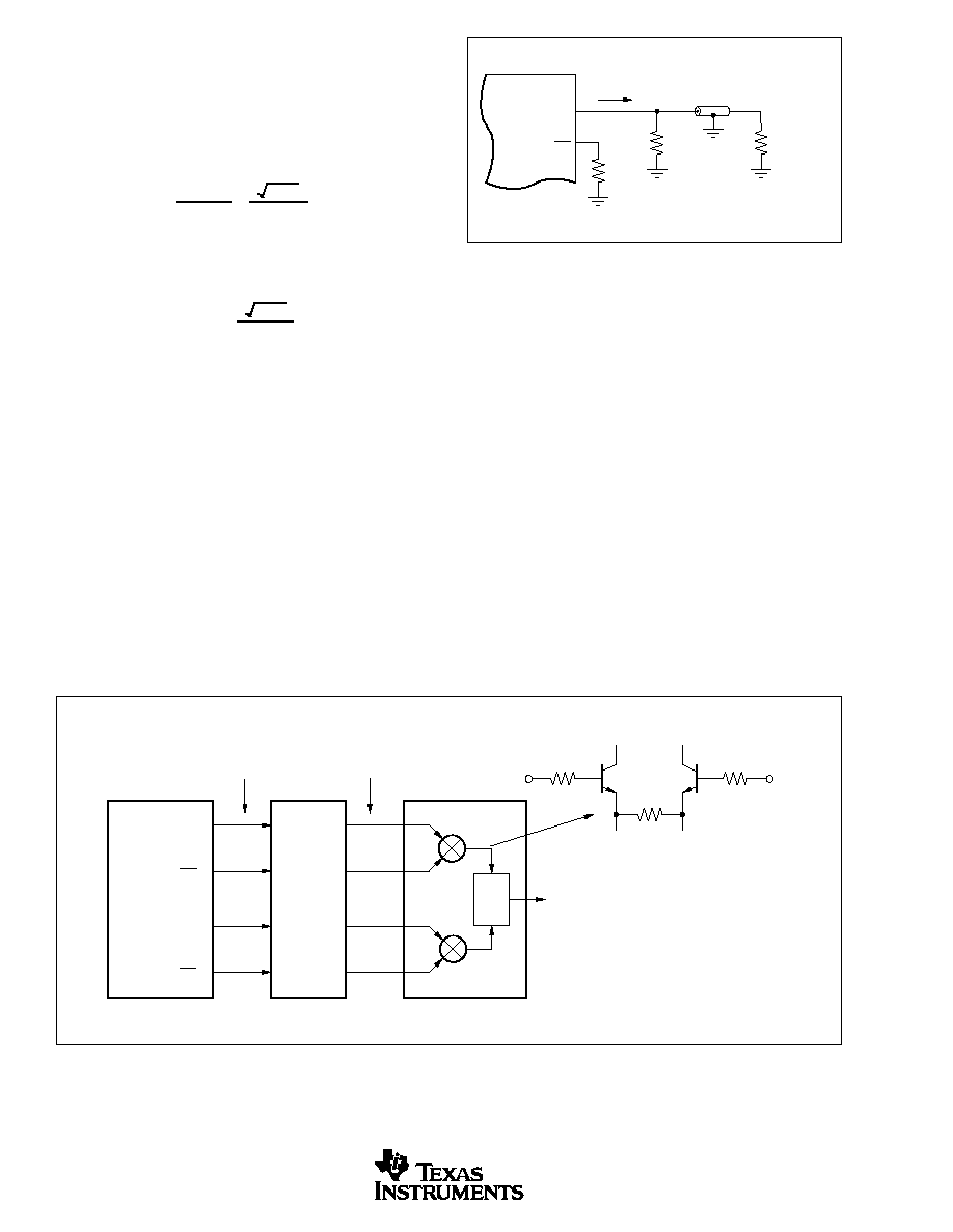
QUADRATURE MODULATORS
One of the main applications for the dual-channel DAC is
baseband I- and Q-channel transmission for digital commu-
nications. In this application, the DAC is followed by an
analog quadrature modulator, modulating an IF carrier with
the baseband data, as shown in Figure 7. Often, the input
stages of these quadrate modulators consist of npn-type
transistors that require a DC bias (base) voltage of > 0.8V.
The wide output compliance range (≠10V to +1.25V) allows
for a direct DC≠coupling between the DAC2902 and the
quadrature modulator.
FIGURE 6. Driving a Doubly Terminated 50
Cable Directly.
FIGURE 7. Generic Interface to a Quadrature Modulator. Signal Conditioning (Level-Shifting) May Be Required to Ensure
Correct DC Common-Mode Levels At the Input of the Quadrature Modulator.
I
OUT
I
OUT
DAC2902
25
50
50
I
OUTFS
= 20mA
V
OUT
= 0V to +0.5V
I
OUT
1
I
OUT
1
I
OUT
2
I
OUT
2
DAC2902
Signal
Conditioning
I
IN
I
REF
Q
IN
Q
REF
Quadrature Modulator
V
OUT
~ 0Vp to 1.20Vp
V
IN
~ 0.6Vp to 1.8Vp
RF
I
IN
I
REF
DAC2902
13
SBAS167A
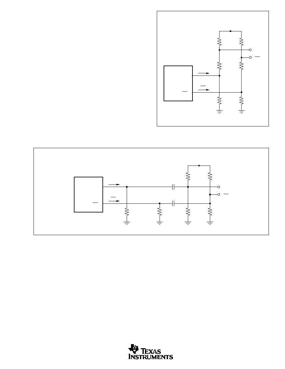
Figure 8 shows an example of a DC-coupled interface with
DC level-shifting, using a precision resistor network. An ac-
coupled interface, as shown in Figure 9, has the advantage
that the common-mode levels at the input of the modulator
can be set independently of those at the output of the DAC.
Furthermore, no voltage loss is obtained in this setup.
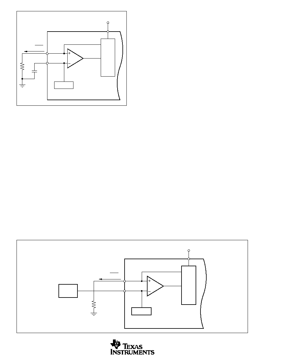
INTERNAL REFERENCE OPERATION
The DAC2902 has an on-chip reference circuit that com-
prises a 1.25V bandgap reference and two control amplifi-
ers, one for each DAC. The full-scale output current, I
OUTFS
,
of the DAC2902 is determined by the reference voltage,
V
REF
, and the value of resistor R
SET
. I
OUTFS
can be calcu-
lated by:
I
OUTFS
= 32 ∑ I
REF
= 32 ∑ V
REF
/ R
SET
(10)
The external resistor R
SET
connects to the FSA pin (Full-
Scale Adjust), see Figure 10. The reference control amplifier
operates as a V-to-I converter producing a reference current,
I
REF
, which is determined by the ratio of V
REF
and R
SET
(as
shown in Equation 10). The full-scale output current, I
OUTFS
,
results from multiplying I
REF
by a fixed factor of 32.
I
OUT
1
I
OUT
1
DAC2902
I
OUT
1
I
OUT
1
V
OUT
1
V
DC
R
3
R
4
R
5
V
OUT
1
FIGURE 8. DC-Coupled Interface to Quadrature Modulator
Applying Level Shifting.
FIGURE 9. AC-Coupled Interface to Quadrature Modulator Applying Level Shifting.
I
OUT
1
I
OUT
1
DAC2902
I
OUT
1
I
OUT
1
V
OUT
1
0.01
µ
F
0.01
µ
F
V
DC
R
1
R
2
V
OUT
1
R
LOAD
50
50
DAC2902
14
SBAS167A
Using the internal reference, a 2k
resistor value results in
a full-scale output of approximately 20mA. Resistors with a
tolerance of 1% or better should be considered. Selecting
higher values, the output current can be adjusted from 20mA
down to 2mA. Operating the DAC2902 at lower than 20mA
output currents may be desirable for reasons of reducing the
total power consumption, optimizing the distortion perfor-
mance, or observing the output compliance voltage limita-
tions for a given load condition.
It is recommended to bypass the REF
IN
pin with a ceramic
chip capacitor of 0.1µF or more. The control amplifier is
internally compensated, and its small signal bandwidth is
approximately 0.3MHz.
GAIN SETTING OPTIONS
The full-scale output current on the DAC2902 can be set two
ways: either for each of the two DAC channels independently
or for both channels simultaneously. For the independent gain
set mode, the GSET pin (pin 42) must be LOW (i.e. connected
to AGND). In this mode, two external resistors are required--
one R
SET
connected to the FSA1 pin (pin 44) and the other to
the FSA2 pin (pin 41). In this configuration, the user has the
flexibility to set and adjust the full-scale output current for each
DAC independently, allowing for the compensation of possible
gain mismatches elsewhere within the transmit signal path.
Alternatively, bringing the GSET pin HIGH (i.e. connected to
+V
A
), the DAC2902 will switch into the simultaneous gain set
mode. Now the full-scale output current of both DAC chan-
nels is determined by only one external R
SET
resistor con-
nected to the FSA1 pin. The resistor at the FSA2 pin may be
removed, however this is not required since this pin is not
functional in this mode and the resistor has no effect to the
gain equation. The formula for deriving the correct R
SET
remains unchanged, e.g. R
SET
= 2k˝ will result in a 20mA
output for both DACs.
EXTERNAL REFERENCE OPERATION
The internal reference can be disabled by simply applying an
external reference voltage into the REF
IN
pin, which in this
case functions as an input, as shown in Figure 11. The use
of an external reference may be considered for applications
that require higher accuracy and drift performance, or to add
the ability of dynamic gain control.
While a 0.1µF capacitor is recommended to be used with the
internal reference, it is optional for the external reference
operation. The reference input, REF
IN
, has a high input
impedance (1M
) and can easily be driven by various
sources. Note that the voltage range of the external reference
should stay within the compliance range of the reference
input (0.5V to 1.25V).
POWER-DOWN MODE
The DAC2902 features a power-down function that can be
used to reduce the total supply current to less than 6mA.
Applying a logic HIGH to the PD pin will initiate the power-
down mode, while a logic LOW enables normal operation.
When left unconnected, an internal active pull-down circuit
will enable the normal operation of the converter.
FIGURE 10. Internal Reference Configuration.
FIGURE 11. External Reference Configuration.
DAC2902
+1.25V Ref.
R
SET
2k
0.1
µ
F
FSA
+5V
+V
A
REF
IN
Current
Sources
I
REF
=
V
REF
R
SET
Ref
Control
Amp
R
SET
External
Reference
I
REF
=
V
REF
R
SET
DAC2902
+1.25V Ref.
FSA
+5V
+V
A
REF
IN
Current
Sources
Ref
Control
Amp

DAC2902
15
SBAS167A
GROUNDING, DECOUPLING, AND
LAYOUT INFORMATION
Proper grounding and bypassing, short lead length, and the use
of ground planes are particularly important for high-frequency
designs. Multilayer PCBs are recommended for best perfor-
mance since they offer distinct advantages such as minimiza-
tion of ground impedance, separation of signal layers by
ground layers, etc.
The DAC2902 uses separate pins for its analog and digital
supply and ground connections. The placement of the decou-
pling capacitor should be such that the analog supply (+V
A
)
is bypassed to the analog ground (AGND), and the digital
supply bypassed to the digital ground (DGND). In most
cases 0.1µF ceramic chip capacitors at each supply pin are
adequate to provide a low impedance decoupling path. Keep
in mind that their effectiveness largely depends on the
proximity to the individual supply and ground pins. There-
fore, they should be located as close as physically possible
to those device leads. Whenever possible, the capacitors
should be located immediately under each pair of supply/
ground pins on the reverse side of the pc board. This layout
approach will minimize the parasitic inductance of compo-
nent leads and PCB runs.
Further supply decoupling with surface-mount tantalum ca-
pacitors (1µF to 4.7µF) may be added as needed in proxim-
ity of the converter.
Low noise is required for all supply and ground connections
to the DAC2902. It is recommended to use a multilayer PCB
utilizing separate power and ground planes. Mixed signal
designs require particular attention to the routing of the
different supply currents and signal traces. Generally, analog
supply and ground planes should only extend into analog
signal areas, such as the DAC output signal and the refer-
ence signal. Digital supply and ground planes must be
confined to areas covering digital circuitry, including the
digital input lines connecting to the converter, as well as the
clock signal. The analog and digital ground planes should be
joined together at one point underneath the DAC. This can
be realized with a short track of approximately 1/8" (3mm).
The power to the DAC2902 should be provided through the
use of wide PCB runs or planes. Wide runs will present a
lower trace impedance, further optimizing the supply decou-
pling. The analog and digital supplies for the converter
should only be connected together at the supply connector of
the pc board. In the case of only one supply voltage being
available to power the DAC, ferrite beads along with bypass
capacitors may be used to create an LC filter. This will
generate a low-noise analog supply voltage that can then be
connected to the +V
A
supply pin of the DAC2902.
While designing the layout, it is important to keep the analog
signal traces separated from any digital line, in order to
prevent noise coupling onto the analog signal path.

DAC2902
16
SBAS167A
PACKAGE DRAWINGS

IMPORTANT NOTICE
Texas Instruments Incorporated and its subsidiaries (TI) reserve the right to make corrections, modifications,
enhancements, improvements, and other changes to its products and services at any time and to discontinue
any product or service without notice. Customers should obtain the latest relevant information before placing
orders and should verify that such information is current and complete. All products are sold subject to TI's terms
and conditions of sale supplied at the time of order acknowledgment.
TI warrants performance of its hardware products to the specifications applicable at the time of sale in
accordance with TI's standard warranty. Testing and other quality control techniques are used to the extent TI
deems necessary to support this warranty. Except where mandated by government requirements, testing of all
parameters of each product is not necessarily performed.
TI assumes no liability for applications assistance or customer product design. Customers are responsible for
their products and applications using TI components. To minimize the risks associated with customer products
and applications, customers should provide adequate design and operating safeguards.
TI does not warrant or represent that any license, either express or implied, is granted under any TI patent right,
copyright, mask work right, or other TI intellectual property right relating to any combination, machine, or process
in which TI products or services are used. Information published by TI regarding third≠party products or services
does not constitute a license from TI to use such products or services or a warranty or endorsement thereof.
Use of such information may require a license from a third party under the patents or other intellectual property
of the third party, or a license from TI under the patents or other intellectual property of TI.
Reproduction of information in TI data books or data sheets is permissible only if reproduction is without
alteration and is accompanied by all associated warranties, conditions, limitations, and notices. Reproduction
of this information with alteration is an unfair and deceptive business practice. TI is not responsible or liable for
such altered documentation.
Resale of TI products or services with statements different from or beyond the parameters stated by TI for that
product or service voids all express and any implied warranties for the associated TI product or service and
is an unfair and deceptive business practice. TI is not responsible or liable for any such statements.
Mailing Address:
Texas Instruments
Post Office Box 655303
Dallas, Texas 75265
Copyright
2002, Texas Instruments Incorporated