Document Outline
- FEATURES
- APPLICATIONS
- DESCRIPTION
- ORDERING INFORMATION
- ABSOLUTE MAXIMUM RATINGS
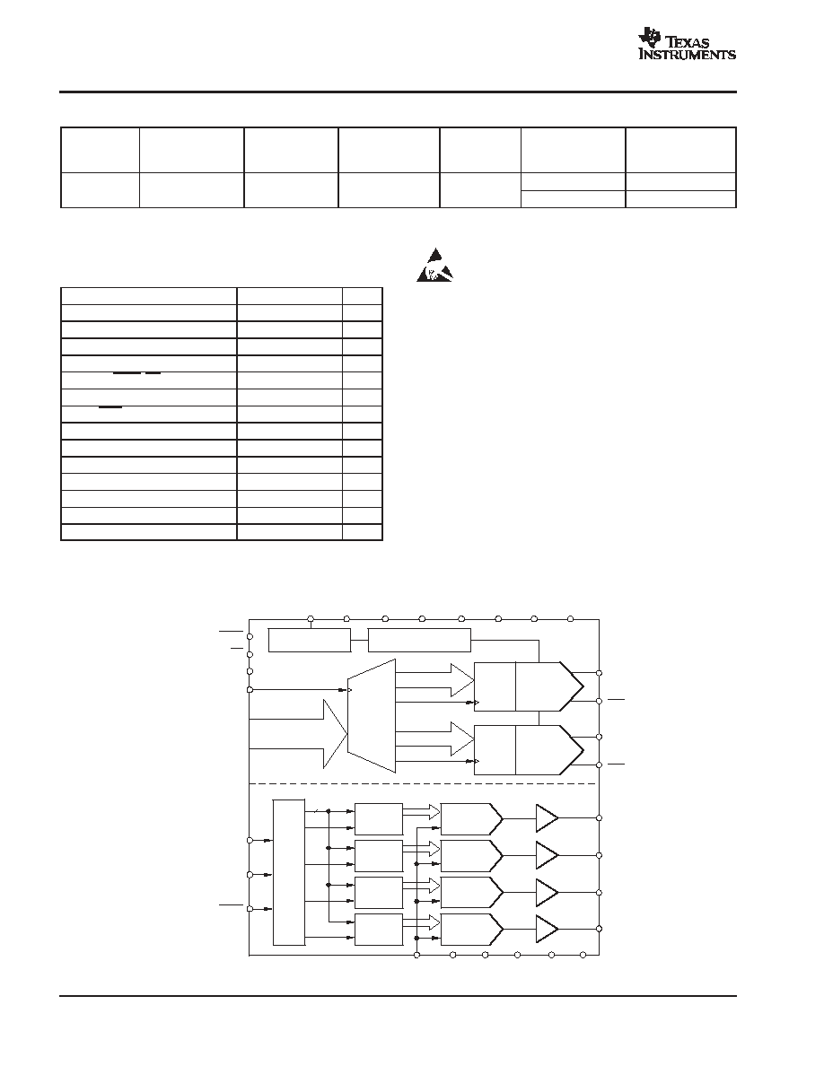
- FUNCTIONAL BLOCK DIAGRAM
- ELECTRICAL CHARACTERISTICS: I-DAC
- ELECTRICAL CHARACTERISTICS: V-DAC
- TIMING INFORMATION
- TIMING REQUIREMENTS(1,2): I-DAC
- TIMING REQUIREMENTS(1,2): V-DAC
- V-DAC: SERIAL DATA INPUT FORMAT
- PIN ASSIGNMENTS
- Terminal Functions
- TYPICAL CHARACTERISTICS
- APPLICATION INFORMATION
- THEORY OF OPERATION
- DAC TRANSFER FUNCTION
- POWER-DOWN MODES
- ANALOG OUTPUTS
- OUTPUT CONFIGURATIONS
- DIFFERENTIAL WITH TRANSFORMER
- DIFFERENTIAL CONFIGURATION USING AN OP AMP
- DUAL TRANSIMPEDANCE OUTPUT CONFIGURATION
- SINGLE-ENDED CONFIGURATION
- INTERFACING ANALOG QUADRATURE MODULATORS
- INTERNAL REFERENCE OPERATION
- GAIN SETTING OPTIONS
- EXTERNAL REFERENCE OPERATION
- V-DAC
- SERIAL INTERFACE
- INPUT SHIFT REGISTER
- SYNC INTERRUPT
- POWER-ON RESET
- GROUNDING, DECOUPLING, AND LAYOUT INFORMATION

SBAS279C - AUGUST 2003 - REVISED OCTOBER 2004
Dual, 12 Bit, 40MSPS
Digital to Analog Converter
DAC2932
FEATURES
D
Dual, 12-Bit, 40MSPS Current Output DAC
D
Four 12-Bit Voltage Output DACs--for
Transmit Control
D
Single +3V Operation
D
Very Low Power: 29mW
D
High SFDR: 75dB at f
OUT
= 5MHz
D
Low-Current Standby or Full Power-Down
Modes
D
Internal Reference
D
Optional External Reference
D
Adjustable Full-Scale Range: 0.5mA to 2mA
APPLICATIONS
D
Transmit Channels
- I and Q
- PC Card Modems: GPRS, CDMA
- Wireless Network Cards (NICs)
D
Signal Synthesis (DDS)
D
Portable Medical Instumentation
D
Arbitrary Waveform Generation (AWG)
DESCRIPTION
The DAC2932 is a dual 12-bit, current-output
digital-to-analog converter (DAC) designed to combine the
features of high dynamic range and very low power
consumption. The DAC2932 converter supports update
rates of up to 40MSPS. In addition, the DAC2932 features
four 12-bit voltage output DACs, which can be used to
perform system control functions.
The advanced segmentation architecture of the DAC2932
is optimized to provide a high spurious-free dynamic range
(SFDR).
The DAC2932 has a high impedance (> 200k
) differential
current output with a nominal range of 2mA and a
compliance voltage of up to 0.8V. The differential outputs
allow for either a differential or single-ended analog signal
interface. The close matching of the current outputs
ensures superior dynamic performance in the differential
configuration, which can be implemented with a
transformer. Using a small geometry CMOS process, the
monolithic DAC2932 is designed to operate within a
single-supply range of 2.7V to 3.3V. Low power
consumption makes it ideal for portable and
battery-operated systems. Further optimization by
lowering the output current can be realized with the
adjustable full-scale option. The full-scale output current
can be adjusted over a span of 0.5mA to 2mA.
For noncontinuous operation of the DAC2932, a full
power-down mode can reduce the power dissipation to as
little as 25
�
W.
The DAC2932 is designed to operate with a single parallel
data port. While it alternates the loading of the input data
into separate input latches for both current output DACs
(I-DACs), the updating of the analog output signal occurs
simultaneously. The DAC2932 integrates a temperature
compensated 1.22V bandgap reference. The DAC2932
also allows for additional flexibility of using an external ref-
erence.
The DAC2932 is available in a TQFP-48 package.
PRODUCTION DATA information is current as of publication date. Products
conform to specifications per the terms of Texas Instruments standard warranty.
Production processing does not necessarily include testing of all parameters.
www.ti.com
Copyright
2003-2004, Texas Instruments Incorporated
Please be aware that an important notice concerning availability, standard warranty, and use in critical applications of Texas Instruments
semiconductor products and disclaimers thereto appears at the end of this data sheet.
All trademarks are the property of their respective owners.
DAC2932
SBAS279C - AUGUST 2003 - REVISED OCTOBER 2004
www.ti.com
2
ORDERING INFORMATION
PRODUCT
PACKAGE-LEAD
PACKAGE
DESIGNATOR(1)
SPECIFIED
TEMPERATURE
RANGE
PACKAGE
MARKING
ORDERING
NUMBER
TRANSPORT
MEDIA, QUANTITY
DAC2932
TQFP-48
PFB
-40
�
C to +85
�
C
DAC2932
DAC2932PFBT
Tape and Reel, 250
DAC2932
TQFP-48
PFB
-40
�
C to +85
�
C
DAC2932
DAC2932PFBR
Tape and Reel, 2000
(1) For the most current specification and package information, refer to our web site at www.ti.com.
ABSOLUTE MAXIMUM RATINGS
over operating free-air temperature range unless otherwise noted
DAC2932
UNIT
+VA to AGND
-0.3 to +4
V
+VD to DGND
-0.3 to +4
V
AGND to DGND
-0.2 to +0.2
V
+VA to +VD
-0.7 to +0.7
V
CLK, PD, STBY, CS to DGND
-0.3 to VD + 0.3
V
D0-D11 to DGND
-0.3 to VD + 0.3
V
IOUT, IOUT to AGND
-0.5 to VA + 0.3
V
REFV to AGNDV
-0.3 to VAV + 0.3
V
GSET, REFIN, FSA to AGND
-0.3 to VA + 0.3
V
VOUTx to AGNDV
-0.3 to VAV + 0.3
V
DIN to DGNDV
-0.3 to VDV + 0.3
V
Junction temperature
+150
�
C
Case temperature
+100
�
C
Storage temperature range
-40 to +150
�
C
This integrated circuit can be damaged by ESD. Texas
Instruments recommends that all integrated circuits be
handled with appropriate precautions. Failure to observe
proper handling and installation procedures can cause damage.
ESD damage can range from subtle performance degradation to
complete device failure. Precision integrated circuits may be more
susceptible to damage because very small parametric changes could
cause the device not to meet its published specifications.
FUNCTIONAL BLOCK DIAGRAM
STBY
CS
DIN
SCLK
SYNC
PD
CLK
Parallel Data Input,
[D0:D11]
12-Bit Data,
Interleaved
DAC2932
REF
IN
+V
D
+V
A
GSET
FSA1
FSA2
AGND
DGND
I
OUT1
I
OUT1
I
OUT2
I
OUT2
V
OUT1
V
OUT2
V
OUT3
V
OUT4
+1.22V Reference
Latch
S
e
r
i
al
-
t
o-
Pa
r
a
ll
e
l
Sh
if
t
R
e
g
is
t
e
r
I
n
put
Lat
c
h
an
d
De
-
Mu
l
t
i
p
l
e
x
e
r
Reference Control Amp
12-Bit
40MSPS
I-DAC1
DAC
Latch 1
12-Bit
40MSPS
I-DAC2
12-Bit
String-DAC1
Latch
12-Bit
String-DAC2
Latch
12-Bit
String-DAC3
Latch
12-Bit
String-DAC4
DAC
Latch 2
Data2
CLK2
Clock
I-DAC Section
A0
A
A
A
A
Dx
12
A1
A2
A3
REFV
+V
DV
+V
AV
AGNDV
DGNDV
PDV
V-DAC Section
Data1
CLK1

DAC2932
SBAS279C - AUGUST 2003 - REVISED OCTOBER 2004
www.ti.com
3
ELECTRICAL CHARACTERISTICS: I-DAC
At TA = TMIN to TMAX (typical values are at TA = 25
�
C), +VA = +3V, +VD = +3V, Update Rate = 40MSPS, IOUTFS = 2mA, RL = 250
, CL
10pF,
GSET = H, and internal reference, unless otherwise noted.
DAC2932
PARAMETER
TEST CONDITIONS
MIN
TYP
MAX
UNITS
Resolution
12
Bits
Output update rate (fCLOCK)
40
MSPS
Specified temperature range, operating
Ambient, TA
-40
+85
�
C
Static Accuracy(1)(2)
Differential nonlinearity (DNL)
-3.5
�
0.5
+3.5
LSB
Integral nonlinearity (INL)
-8
�
1.5
+8
LSB
Dynamic Performance(3)
Spurious-free dynamic range (SFDR)
To Nyquist, 0dBFS
fOUT = 0.2MHz, fCLOCK = 20MSPS
68
dBc
fOUT = 0.55MHz, fCLOCK = 40MSPS
71
dBc
fOUT = 1MHz, fCLOCK = 25MSPS(4)
58
70
dBc
fOUT = 2.2MHz, fCLOCK = 40MSPS
72
dBc
fOUT = 5MHz, fCLOCK = 40MSPS
75
dBc
fOUT = 10MHz, fCLOCK = 40MSPS
69
dBc
fOUT = 20MHz, fCLOCK = 40MSPS
57
dBc
Spurious-free dynamic range within a
window
fOUT = 2.2MHz, fCLOCK = 40MSPS
1MHz span
76
dBc
fOUT = 10MHz, fCLOCK = 40MSPS
2MHz span
74
dBc
Total harmonic distortion (THD)
fOUT = 0.55MHz, fCLOCK = 40MSPS
-70
dBc
fOUT = 1MHz, fCLOCK = 25MSPS(4)
-58
-69
dBc
fOUT = 2.2MHz, fCLOCK = 40MSPS
-70
dBc
Signal-to-noise and distortion (SINAD)
fOUT = 1MHz, fCLOCK = 25MSPS(4)
52
61
dBc
Output settling time(1)
to 0.1%
20
ns
Output rise time(1)
10% to 90%
7.7
ns
Output fall time(1)
10% to 90%
7.4
ns
DC Accuracy
Full-scale output range(5)(6) (FSR)
All bits high, IOUT1, IOUT2
0.5
2
mA
Output compliance range(7), VCO
-0.5
+0.5
+0.8
V
Gain error (Full-Scale)
-2
�
0.5
+2
%FSR
Gain error drift
70
ppmFSR/
�
C
Gain matching
-2.5
+0.6
+2.5
%FSR
Offset error
�
0.001
%FSR
Power-supply rejection, +VA
+3V,
�
10%, at 25
�
C
-0.9
+0.5
+0.9
%FSR/V
Power-supply rejection, +VD
+3V,
�
10%, at 25
�
C
-0.12
+0.03
+0.12
%FSR/V
Output resistance
200
k
Output capacitance
IOUT, IOUT to Ground
5
pF
(1) At output IOUT1, IOUT2, while driving a 250
load, transition from 000h to FFFh.
(2) Measured at fCLOCK = 25MSPS and fOUT = 1.0MHz.
(3) Differential, transformer (n = 4:1) coupled output, RL = 400
.
(4) Differential outputs with a 250
load.
(5) Nominal full-scale output current is I
OUTFS
+
32
I
REF
+
32
V
REF
R
SET
; with V
REF
+
1.22V (typ) and R
SET
+
19.6k
W
(1%)
(6) Ensured by design and characterization; not production tested.
(7) Gain error to remain
10% FSR over the full compliance range.
(8) Combined power dissipation of I-DAC and V-DAC.
DAC2932
SBAS279C - AUGUST 2003 - REVISED OCTOBER 2004
www.ti.com
4
ELECTRICAL CHARACTERISTICS: I-DAC (continued)
At TA = TMIN to TMAX (typical values are at TA = 25
�
C), +VA = +3V, +VD = +3V, Update Rate = 40MSPS, IOUTFS = 2mA, RL = 250
, CL
10pF,
GSET = H, and internal reference, unless otherwise noted.
DAC2932
PARAMETER
UNITS
MAX
TYP
MIN
TEST CONDITIONS
Reference
Voltage, VREF
+1.14
+1.22
+1.26
V
Tolerance
�
30
mV
Voltage drift
-40
ppm/
�
C
Output current
10
�
A
Input resistance
1
M
Input compliance range
External VREF
+1.22
V
Small-signal bandwidth
0.1
MHz
Digital Inputs(6)
Logic coding
Straight binary
Logic high voltage, VIH
+2
+3
V
Logic low voltage, VIL
0
+0.8
V
Logic high current
�
1
�
A
Logic low current
�
1
�
A
Input capacitance
5
pF
Power Supply
Analog supply voltage, +VA, +VAV
2.7
3
3.3
V
Digital supply voltage, +VD, +VDV
2.7
3
3.3
V
Analog supply current, IVA
fCLOCK = 25MSPS, digital inputs at 0
4.7
mA
IVA
fCLOCK = 40MSPS, fOUT = 2.2MHz
5.4
mA
IVA
Standby mode
0.4
mA
Digital supply current, IVD
fCLOCK = 25MSPS, digital inputs at 0
2
mA
lVD
fCLOCK = 40MSPS, fOUT = 2.2MHz
4.3
mA
IVD
Standby mode, clock off
0.02
mA
IVD
Standby mode, CS = 0, fCLOCK = 25MSPS
1.3
mA
Power dissipation, PD(8)
fCLOCK = 25MSPS, digital inputs at 0
20
25
mW
PD
fCLOCK = 40MSPS, fOUT = 2.2MHz
29
mW
PD
Standby mode, fCLOCK = 25MSPS
5.5
7
mW
PD
Power-down mode, clock off, digital inputs at 0
25
�
W
Thermal resistance
TQFP-48
JA
97.5
�
C/W
TQFP-48
JC
20
�
C/W
(1) At output IOUT1, IOUT2, while driving a 250
load, transition from 000h to FFFh.
(2) Measured at fCLOCK = 25MSPS and fOUT = 1.0MHz.
(3) Differential, transformer (n = 4:1) coupled output, RL = 400
.
(4) Differential outputs with a 250
load.
(5) Nominal full-scale output current is I
OUTFS
+
32
I
REF
+
32
V
REF
R
SET
; with V
REF
+
1.22V (typ) and R
SET
+
19.6k
W
(1%)
(6) Ensured by design and characterization; not production tested.
(7) Gain error to remain
10% FSR over the full compliance range.
(8) Combined power dissipation of I-DAC and V-DAC.

DAC2932
SBAS279C - AUGUST 2003 - REVISED OCTOBER 2004
www.ti.com
5
ELECTRICAL CHARACTERISTICS: V-DAC
At TA = TMIN to TMAX (typical values are at TA = 25
�
C), +VAV = +3V, +VDV = +3V, RL = 2k
to GND, and CL = 40pF, unless otherwise noted.
DAC2932
PARAMETER
TEST CONDITIONS
MIN
TYP
MAX
UNITS
Static Performance(1)
Resolution
12
Bits
Relative accuracy
At 25
�
C
-16
�
8
+16
LSB
Differential nonlinearity, DNL
Tested; monotonic by design
-1
�
0.2
+1
LSB
Zero code error(2)
All 0s loaded to DAC register
0.2
+0.8
%FSR
Full-scale error(2)
All 1s loaded to DAC register
-10
-3
+2
%FSR
Zero code error drift
5
�
V/
�
C
Full-scale error drift
-15
ppmFSR/
�
C
Output Characteristics(3)
Reference voltage setting, REFV
0
+VAV
V
Output voltage settling time
1/4 scale to 3/4 scale change (400h to C00h)
3
�
s
CL = 470pF
5
�
s
Slew rate
1
V/
�
s
Capacitive load stability
RL = 2k
470
pF
Code change glitch impulse
1LSB change around major carry
11
nV-s
Digital feedthrough
0.5
nV-s
DC output impedance
4
Short-circuit current
20
mA
Power-up time
Coming out of power-down mode
8
�
s
Logic Inputs(3)
Input current
�
1
�
A
Input low voltage, VIL
0
0.8
V
Input high voltage, VIH
2
3
V
Input capacitance
5
pF
(1) Linearity calculated using a reduced code range of 48 to 3976.
(2) Full-scale range (FSR) based on reference REFV = +VAV = +3.0V.
(3) Ensured by design and characterization; not production tested.

DAC2932
SBAS279C - AUGUST 2003 - REVISED OCTOBER 2004
www.ti.com
6
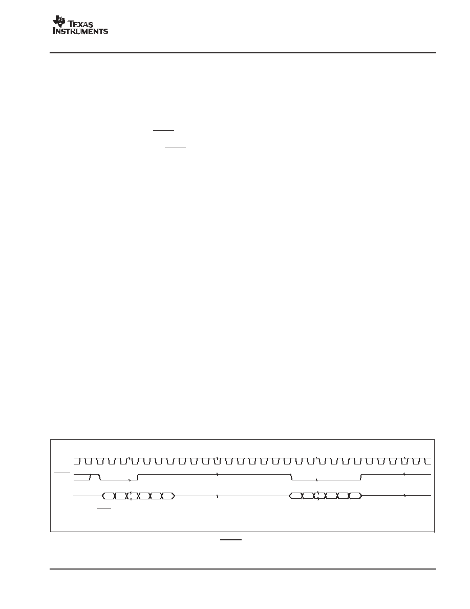
TIMING INFORMATION
t
CP
t
CL
t
DO2
t
DO1
t
S1
t
S2
t
H1
t
H2
t
CH
DAC1 (n
-
1)
CLK
Data In[D0:D11]
I-DAC OUT1
I-DAC OUT2
DAC2 (n
-
1)
DAC2 (n)
DAC2 (n + 1)
DAC1 (n)
DAC1 (n +1)
(n
-
2)
(n
-
2)
(n
-
1)
(n
-
1)
(n)
(n)
Figure 1. Timing Diagram of I-DAC
TIMING REQUIREMENTS
(1,2)
: I-DAC
PARAMETER
DESCRIPTION
MIN
TYP
MAX
UNIT
tCP
Clock cycle time (period)
25
ns
tCL
Clock low time
10
ns
tCH
Clock high time
10
ns
tS1
Data setup time, I-DAC1
0.5
5
ns
tS2
Data setup time, I-DAC2
0.5
5
ns
tH1
Data hold time, I-DAC1
2.2
5
ns
tH2
Data hold time, I-DAC2
2.2
5
ns
tDO1(3)
Output delay time, I-DAC1
tS1 + tCP
ns
tDO2(3)
Output delay time, I-DAC2
tS2+(tCP/2)
ns
CS hold time (pulse width)
tCP + 3.5
ns
CS to clock rising or falling edge setup time
-1.5
ns
STBY rise time to IOUT
17
�
s
PD fall time to IOUT (I-DAC coming out of power-down mode)
22
�
s
(1) Based on design simulation and characterization; not production tested.
(2) All input signals are specified with tr = tf
2ns (10% to 90% of +VDV) and timed from a voltage level of (VIL + VIH)/2.
(3) Output delay time measured from 50% of rising clock edge to 50% point of full-scale transition.

DAC2932
SBAS279C - AUGUST 2003 - REVISED OCTOBER 2004
www.ti.com
7
SCLK
DB15
DB0
SYNC
DIN
t
1
t
2
t
7
t
3
t
4
t
8
t
5
t
6
Figure 2. Serial Write Operation of V-DAC
TIMING REQUIREMENTS
(1,2)
: V-DAC
PARAMETER
DESCRIPTION
MIN
TYP
MAX
UNIT
t1(3)
SCLK cycle time
50
ns
t2
SCLK high time
13
ns
t3
SCLK low time
22.5
ns
t4
SYNC to SCLK rising edge setup time
0
ns
t5
Data setup time
5
7.5
ns
t6
Data hold time
1.5
2.5
ns
t7
SCLK falling edge to SYNC rising edge
0
-6.0
ns
t8
Minimum SYNC high time
50
ns
PDV fall time to VOUT (V-DAC coming out of power-down mode)
8
�
s
(1) All input signals are specified with tr = tf
2ns (10% to 90% of +VDV) and timed from a voltage level of (VIL + VIH)/2.
(2) Based on design simulation and characterization; not production tested.
(3) Maximum SCLK frequency is 20MHz at +VAV = +VDV = +2.7V to 3.3V.
V-DAC: SERIAL DATA INPUT FORMAT
DB15
DB14
DB13
DB12
DB11
DB10
DB9
DB8
DB7
DB6
DB5
DB4
DB3
DB2
DB1
DB0
A0
DAC1
A1
DAC2
A2
DAC3
A3
DAC4
D11
(MSB)
D10
D9
D8
D7
D6
D5
D4
D3
D2
D1
D0
(LSB)
Address Bits
12-Bit Data Word
NOTE: A logic high in the address bit will select the corresponding V-DAC and write the data word into its register. If more than one address bit
is set high, the selected V-DACs are updated with the same data word simultaneously.

DAC2932
SBAS279C - AUGUST 2003 - REVISED OCTOBER 2004
www.ti.com
8
PIN ASSIGNMENTS
36
35
34
33
32
31
30
29
28
27
26
25
1
2
3
4
5
6
7
8
9
10
11
12
48
47
46
45
44
43
42
41
40
39
38
13
14
15
16
17
18
19
20
21
22
23
37
24
DAC2932
(V-DAC Section)
NC
+V
AV
I
OUT2
I
OUT2
AGND
+V
A
I
OUT1
I
OUT1
REF
IN
DG
NDV
SY
N
C
SC
L
K
DIN
PD
V
RE
F
V
+V
DV
A
G
NDV
V
OU
T
4
V
OU
T
3
V
OU
T
2
V
OU
T
1
DG
ND
+V
D
CL
K
PD
ST
BY
CS
GS
E
T
DG
ND
AG
N
D
FS
A
2
FS
A
1
Bit_1 (MSB)
Bit_2
Bit_3
Bit_4
Bit_5
Bit_6
Bit_7
Bit_8
Bit_9
Bit_10
Bit_11
Bit_12 (LSB)
+V
A
AGND
AGND
AG
N
D
Terminal Functions
TERMINAL
NAME
NO.
I/O
DESCRIPTION
D0:D11
1:12
I
Parallel data input port for the dual I-DACs; MSB = D11, LSB = D0; interleaved operation.
DGND
13
Digital ground of I-DAC
+VD
14
Digital supply of I-DAC; 2.7V to 3.3V
CLK
15
I
Clock input of I-DAC
PD
16
I
Power-down pin; active high; a logic high initiates power-down mode.
STBY
17
I
Standby pin of I-DAC; active low; a logic low initiates Standby mode with PD = Low.
A logic high configures the I-DAC for normal operation; pin will resume a high state if left open.
CS
18
I
Chip select; active low; enables the parallel data port of the I-DACs.
Pin will resume a low state if left open.
GSET
19
I
Gain-setting mode. A logic high enables the use of two separate full-scale adjust resistors on pins FSA1
and FSA2. A logic low allows the use of a common full-scale adjust resistor connected to FSA1. The
function of the FSA2 pin is disabled, and any remaining resistor has no effect. The value for the RSET
resistor remains the same for a given full-scale range, regardless of the selected GSET mode. Pin will
resume a low state if left open.
DGND
20
Digital ground of I-DAC
AGND
21
Analog ground of I-DAC
AGND
22
Analog ground of I-DAC
FSA2
23
I
Full-scale adjust of I-DAC2; connect external gain setting resistor RSET2 = 19.6k
.
FSA1
24
I
Full-scale adjust of I-DAC1; connect external gain setting resistor RSET1 = 19.6k
.
REFIN
25
I
External reference voltage input; internal reference voltage output; bypass with 0.1
�
F to AGND for internal
reference operation.

DAC2932
SBAS279C - AUGUST 2003 - REVISED OCTOBER 2004
www.ti.com
9
Terminal Functions (continued)
TERMINAL
NAME
DESCRIPTION
I/O
NO.
IOUT1
26
O
Complementary current ouput of I-DAC1
IOUT1
27
O
Current output of I-DAC1
AGND
28
Analog ground of I-DAC
+VA
29
Analog supply of I-DAC; 2.7V to 3.3V
+VA
30
Analog supply of I-DAC; 2.7V to 3.3V
AGND
31
Analog ground of I-DAC
AGND
32
Analog ground of I-DAC
IOUT2
33
O
Current output of I-DAC2
IOUT2
34
O
Complementary current ouput of I-DAC2
+VAV
35
Analog supply of V-DAC; 2.7V to 3.3V
NC
36
No internal connection
VOUT1
37
O
Voltage output of V-DAC1
VOUT2
38
O
Voltage output of V-DAC2
VOUT3
39
O
Voltage output of V-DAC3
VOUT4
40
O
Voltage output of V-DAC4
AGNDV
41
Analog ground of V-DAC
REFV
42
I
Reference voltage input for V-DACs; typically connected to supply (+VAV)
+VDV
43
Digital supply of V-DAC; 2.7V to 3.3V
PDV
44
I
Power-down of V-DACs; active high; a logic high initiates the power-down mode
DIN
45
I
Serial digital input for V-DAC; see timing and application sections for details
SCLK
46
I
Clock input of V-DAC
SYNC
47
I
Frame synchronization signal for the serial data at DIN. Refer to timing section for details.
DGNDV
48
Digital ground of V-DAC.

DAC2932
SBAS279C - AUGUST 2003 - REVISED OCTOBER 2004
www.ti.com
10
TYPICAL CHARACTERISTICS
TA = +25
�
C, +VA = +VAV = +3V, +VD = +VDV = +3V, IOUTFS = 2mA, differential transformer-coupled output (n = 4:1), RL = 400
on I-DAC,
RL = 2k
on V-DAC, and GSET = H unless otherwise noted.
Figure 3
I-DAC, INL
0
2.0
1.6
1.2
0.8
0.4
0
-
0.4
-
0.8
-
1.2
-
1.6
-
2.0
500
1000
1500
2000
2500
3000
3500 4000
Codes
IN
L
(
L
S
B
)
Figure 4
I-DAC, DNL
0
1.0
0.8
0.6
0.4
0.2
0
-
0.2
-
0.4
-
0.6
-
0.8
-
1.0
500
1000
1500
2000
2500
3000
3500 4000
Codes
DNL
(
L
S
B
)
Figure 5
SFDR vs f
OUT
AT 5MSPS
0
80
78
76
74
72
70
68
66
64
62
60
0.5
1.0
1.5
2.0
2.5
f
OUT
(MHz)
SF
D
R
(
d
Bc
)
Figure 6
SFDR vs f
OUT
AT 10MSPS
0
80
75
70
65
60
55
50
0.5
4.5
1.0
3.5
4.0
5.0
1.5
2.0
2.5
3.0
f
OUT
(MHz)
SF
D
R
(
d
Bc
)
Figure 7
SFDR vs f
OUT
AT 20MSPS
0
80
75
70
65
60
55
50
1
9
2
7
8
10
3
4
5
6
f
OUT
(MHz)
SF
D
R
(
d
Bc
)
Figure 8
SFDR vs f
OUT
AT 40MSPS
0
80
75
70
65
60
55
50
2
18
4
14
16
20
6
8
10
12
f
OUT
(MHz)
SF
D
R
(
d
Bc)

DAC2932
SBAS279C - AUGUST 2003 - REVISED OCTOBER 2004
www.ti.com
11
TYPICAL CHARACTERISTICS (continued)
TA = +25
�
C, +VA = +VAV = +3V, +VD = +VDV = +3V, IOUTFS = 2mA, differential transformer-coupled output (n = 4:1), RL = 400
on I-DAC,
RL = 2k
on V-DAC, and GSET = H unless otherwise noted.
Figure 9
80
75
70
65
60
55
50
SF
D
R
(
d
B
c
)
0
2
4
6
8
10
12
16
14
18
20
f
OUT
(MHz)
SFDR vs I
OUT
FS AND f
OUT
AT 40MSPS, 0dBFS
1.5mA
0.5mA
1mA
2mA
Figure 10
SFDR vs TEMPERATURE
-
40
80
75
70
65
60
55
50
-
30
70
-
20
40
60
50
80 85
-
10
0
10
20
30
Temperature (
_
C)
SF
D
R
(
d
Bc
)
2.2MHz, 40MSPS
1MHz, 20MSPS
10MHz, 40MSPS
19.9MHz, 40MSPS
Figure 11
TOTAL HARMONIC DISTORTION vs
f
CLK
AT f
OUT
= 2.2MHZ
5
-
60
-
65
-
70
-
75
-
80
40
35
30
25
20
15
10
f
CLK
(MSPS)
TH
D
(
d
B
c
)
Figure 12
TOTAL HARMONIC DISTORTION vs TEMPERATURE
f
OUT
= 1MHz at 20MSPS
-
40
-
50
-
55
-
60
-
65
-
70
-
75
-
80
-
85
-
90
-
30
70
-
20
40
60
50
80 85
-
10
0
10
20
30
Temperature (
_
C)
TH
D
(
d
B
c
)
Figure 13
1.223
1.222
1.221
1.220
1.219
1.218
1.217
1.216
1.215
V
RE
F
(V
)
-
40
-
20
0
20
40
60
80 85
Temperature (
_
C)
REFERENCE VOLTAGE vs TEMPERATURE
Figure 14
1.2201
1.2200
1.2199
V
RE
F
(V
)
2.7
2.8
2.9
3.0
3.1
3.2
3.3
Supply Voltage (V)
REFERENCE VOLTAGE vs SUPPLY VOLTAGE

DAC2932
SBAS279C - AUGUST 2003 - REVISED OCTOBER 2004
www.ti.com
12
TYPICAL CHARACTERISTICS (continued)
TA = +25
�
C, +VA = +VAV = +3V, +VD = +VDV = +3V, IOUTFS = 2mA, differential transformer-coupled output (n = 4:1), RL = 400
on I-DAC,
RL = 2k
on V-DAC, and GSET = H unless otherwise noted.
Figure 15
5.60
5.55
5.50
5.45
5.40
5.35
5.30
5.25
5.20
I
A
(m
A
)
-
40
-
20
0
20
40
60
80 85
Temperature (
_
C)
I
A
vs TEMPERATURE
Figure 16
6.5
6.0
5.5
5.0
4.5
4.0
3.5
3.0
2.5
2.0
I
D
(m
A
)
-
40
-
20
0
20
40
60
80 85
Temperature (
_
C)
I
D
vs TEMPERATURE AT f
OUT
AND f
CLK
19.9MHz, 40MSPS
10MHz, 40MSPS
2.2MHz, 40MSPS
1MHz, 20MSPS
Figure 17
5.43
5.42
5.41
5.40
5.39
5.38
5.37
5.36
5.35
I
A
(m
A
)
2.7
2.8
2.9
3.0
3.1
3.2
3.3
Supply Voltage (V)
I
A
vs SUPPLY VOLTAGE
Figure 18
6.5
6.0
5.5
5.0
4.5
4.0
3.5
3.0
2.5
2.0
I
D
(m
A
)
2.7
2.8
2.9
3.0
3.1
3.2
3.3
Supply Voltage (V)
I
D
vs SUPPLY VOLTAGE AT f
OUT
AND f
CLK
19.9MHz, 40MSPS
10MHz, 40MSPS
2.2MHz, 40MSPS
1MHz, 20MSPS
Figure 19
0
-
10
-
20
-
30
-
40
-
50
-
60
-
70
-
80
-
90
-
100
Ma
gni
t
u
de
(
d
B
m
)
0
2
4
6
8
10
12
16
14
18
20
Frequency (MHz)
I-DAC1 OUTPUT SPECTRUM
f
OUT
= 2.2MHz
f
CLK
= 40MSPS
Figure 20
0
-
10
-
20
-
30
-
40
-
50
-
60
-
70
-
80
-
90
-
100
0
2
4
6
8
10
12
16
14
18
20
Magni
tud
e
(
d
B
m
)
Frequency (MHz)
I-DAC2 OUTPUT SPECTRUM
f
OUT
= 2.2MHz
f
CLK
= 40MSPS

DAC2932
SBAS279C - AUGUST 2003 - REVISED OCTOBER 2004
www.ti.com
13
TYPICAL CHARACTERISTICS (continued)
TA = +25
�
C, +VA = +VAV = +3V, +VD = +VDV = +3V, IOUTFS = 2mA, differential transformer-coupled output (n = 4:1), RL = 400
on I-DAC,
RL = 2k
on V-DAC, and GSET = H unless otherwise noted.
Figure 21
-
10
-
20
-
30
-
40
-
50
-
60
-
70
-
80
-
90
-
100
-
110
0
2
4
6
8
10
12
16
14
18
20
M
agn
i
t
ude
(
d
B
m
)
Frequency (MHz)
DUAL-TONE OUTPUT SPECTRUM
f
1
= 1.2MHz
f
2
= 2.2MHz
f
CLK
= 40MSPS
Figure 22
-
10
-
20
-
30
-
40
-
50
-
60
-
70
-
80
-
90
-
100
-
110
0
2
4
6
8
10
12
16
14
18
20
M
agni
tu
d
e
(
d
B
m
)
Frequency (MHz)
FOUR-TONE OUTPUT SPECTRUM
f
1
= 1.2MHz
f
2
= 2.2MHz
f
3
= 3.2MHz
f
4
= 4.2MHz
f
CLK
= 40MSPS
Figure 23
-
60
-
70
-
80
-
90
-
100
-
110
-
120
C
h
annel
Is
ol
a
t
i
o
n
(
d
B
c
)
0
2
4
6
8
10
12
16
14
18
20
Frequency (MHz)
I-DAC CHANNEL ISOLATION vs f
OUT
AT 40MSPS
Channel 1
Channel 2
Figure 24
V-DAC, INL
0
16
12
8
4
0
-
4
-
8
-
12
-
16
500
1000
1500
2000
2500
3000
3500 4000
Codes
IN
L
(
L
S
B
)
Figure 25
V-DAC, DNL
0
1.0
0.8
0.6
0.4
0.2
0
-
0.2
-
0.4
-
0.6
-
0.8
-
1.0
500
1000
1500
2000
2500
3000
3500 4000
Codes
DNL
(
L
S
B
)
Figure 26
V
OUT
vs CODE
0
3.00
2.75
2.50
2.25
2.00
1.75
1.50
1.25
1.00
0.75
0.50
0.25
0
500
1000
1500
2000
2500
3000
3500 4000
Codes
V
OU
T
(V
)
DAC2932
SBAS279C - AUGUST 2003 - REVISED OCTOBER 2004
www.ti.com
14
APPLICATION INFORMATION
THEORY OF OPERATION
The architecture of the DAC2932 uses the current steering
technique to enable fast switching and a high update rate.
The core element within the monolithic DAC is an array of
segmented current sources that are designed to deliver a
full-scale output current of up to 2mA, as shown in
Figure 27. An internal decoder addresses the differential
current switches each time the DAC is updated and a
corresponding output current is formed by steering all
currents to either output summing node, I
OUT
or I
OUT
. The
complementary outputs deliver a differential output signal,
which improves the dynamic performance through
reduction of even-order harmonics and common-mode
signals (noise), and doubles the peak-to-peak output
signal swing by a factor of two, compared to single-ended
operation.
The segmented architecture results in a significant
reduction of the glitch energy, and improves the dynamic
performance (SFDR) and DNL. The current outputs
maintain a very high output impedance of greater than
200k
.
The full-scale output current is determined by the ratio of
the internal reference voltage (approximately +1.2V) and
an external resistor, R
SET
. The resulting I
REF
is internally
multiplied by a factor of 32 to produce an effective DAC
output current that can range from 0.5mA to 2mA,
depending on the value of R
SET
.
The DAC2932 is split into a digital and an analog portion,
each of which is powered through its own supply pin. The
digital section includes edge-triggered input latches and
the decoder logic, while the analog section comprises the
current source array with its associated switches, and the
reference circuitry.
STBY
CS
DIN
SCLK
SYNC
PD
CLK
Parallel Data Input,
[D0:D11]
12-Bit Data,
Interleaved
DAC2932
REF
IN
+V
D
+V
A
GSET
FSA1
FSA2
AGND
DGND
I
OUT1
I
OUT1
I
OUT2
I
OUT2
V
OUT1
V
OUT2
V
OUT3
V
OUT4
+1.22V Reference
Latch
S
e
r
i
al
-
t
o-
Pa
r
a
ll
e
l
Sh
if
t
R
e
g
is
t
e
r
I
n
put
Lat
c
h
an
d
De
-
Mu
l
t
i
p
l
e
x
e
r
Reference Control Amp
12-Bit
40MSPS
I-DAC1
DAC
Latch 1
12-Bit
40MSPS
I-DAC2
12-Bit
String-DAC1
Latch
12-Bit
String-DAC2
Latch
12-Bit
String-DAC3
Latch
12-Bit
String-DAC4
DAC
Latch 2
Data2
CLK2
Clock
I-DAC Section
A0
A
A
A
A
Dx
12
A1
A2
A3
REFV
+V
DV
+V
AV
AGNDV
DGNDV
PDV
V-DAC Section
Data1
CLK1
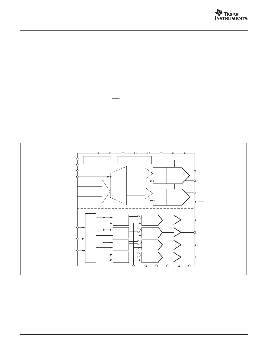
Figure 27. Block Diagram of the DAC2932

DAC2932
SBAS279C - AUGUST 2003 - REVISED OCTOBER 2004
www.ti.com
15
DAC TRANSFER FUNCTION
Each of the I-DACs in the DAC2932 has a complementary
current output, I
OUT1
and I
OUT2
. The full-scale output
current, I
OUTFS
, is the summation of the two
complementary output currents:
I
OUTFS
+
I
OUT
)
I
OUT
The individual output currents depend on the DAC code
and can be expressed as:
I
OUT
+
I
OUTFS
(Code 4096)
I
OUT
+
I
OUTFS
(4095
*
Code) 4096
where Code is the decimal representation of the DAC data
input word (0 to 4095).
Additionally, I
OUTFS
is a function of the reference current
I
REF
, which is determined by the reference voltage and the
external setting resistor, R
SET
.
I
OUTFS
+
32
I
REF
+
32
V
REF
R
SET
In most cases, the complementary outputs will drive
resistive loads or a terminated transformer. A signal
voltage will develop at each output according to:
V
OUT
+
I
OUT
R
LOAD
V
OUT
+
I
OUT
R
LOAD
The value of the load resistance is limited by the output
compliance specification of the DAC2932. To maintain
optimum linearity performance, the compliance voltage at
I
OUT
and I
OUT
should be limited to +0.5V or less.
The two single-ended output voltages can be combined to
find the total differential output swing:
V
OUTDIFF
+
V
OUT
*
V
OUT
+
(2
Code
*
4095)
4096
I
OUTFS
R
LOAD
POWER-DOWN MODES
The DAC2932 has several modes of operation. Besides
normal operation, the I-DAC section features a Standby
mode and a full power-down mode, while the V-DAC
section has one power-down mode. All modes are
controlled by appropriate logic levels on the assigned pins
of the DAC2932. Table 1 lists all pins and possible modes.
The pins have internal pull-ups or pull-downs; if left open,
all pins will resume logic levels that place the I-DAC and
V-DAC in a normal operating mode (fully functional).
When in Standby mode the analog functions of the I-DAC
section are powered down. The internal logic is still active
and will consume some power if the clock remains applied.
To further reduce the power in Standby mode the CS pin
may be pulled high, which disables the internal logic from
being clocked, even with the clock signal applied.
If CS remains low during the Standby mode and a running
clock remains applied, any new data on the parallel data
port will be latched into the DAC. The analog output,
however, will not be updated as long as the I-DACs remain
in Standby mode.
Table 1. Power-Down Modes
PD (16)
STBY(17)
CS (18)
PDV (44)
DAC
MODE
DAC OUTPUTS
0
0
0
X
I-DAC enabled
Standby; data can still be written into the DACs
with running clock applied
High-Z
0
0
1
X
I-DAC disabled
Standby; writing into DAC disabled--clock input
disabled by CS
High-Z
0
1
0
X
I-DAC enabled
Normal operation (return from Standby)
Last state prior to
Standby
0
1
1
X
I-DAC disabled
Data input and clock input disabled; use when
multiple devices on one bus
Last data held
1
X
X
X
I-DAC disabled
Full power-down; STBY and CS have no effect
High-Z
X
X
X
0
V-DAC enabled
V-DAC normal operation
X
X
X
1
V-DAC disabled
V-DAC in power-down mode; independent
operation of any I-DAC power-down
configuration
All outputs; High-Z
NOTE: X = don't care.
(1)
(2)
(3)
(4)
(5)
(6)
(7)

DAC2932
SBAS279C - AUGUST 2003 - REVISED OCTOBER 2004
www.ti.com
16
ANALOG OUTPUTS
The DAC2932 provides two sets of complementary
current outputs, I
OUT
and I
OUT
. The simplified circuit of the
analog output stage representing the differential topology
is shown in Figure 28. The output impedance of I
OUT
and
I
OUT
results from the parallel combination of the differential
switches, along with the current sources and associated
parasitic capacitances.
I
OUT
I
OUT
DAC2932
R
L
R
L
+V
A
Figure 28. Equivalent Analog Output
The signal voltage swing that develops at the two outputs,
I
OUT
and I
OUT
, is limited by a negative and positive
compliance. The negative limit of �0.5V is given by the
breakdown voltage of the CMOS process, and exceeding
it will compromise the reliability of the DAC2932, or even
cause permanent damage. With the full-scale output set to
2mA, the positive compliance equals 0.8V, operating with
an analog supply of +V
A
= 3V. To avoid degradation of the
distortion performance and integral linearity, care must be
taken so that the configuration of the DAC2932 does not
exceed the compliance range.
Best distortion performance is typically achieved with the
maximum full-scale output signal limited to approximately
0.5V
PP
. This is the case for a 250
load and a 2mA
full-scale output current. A variety of loads can be adapted
to the output of the DAC2932 by selecting a suitable
transformer while maintaining optimum voltage levels at
I
OUT
and I
OUT
. Furthermore, using the differential output
configuration in combination with a transformer is
instrumental in achieving excellent distortion
performance. Common-mode errors, such as even-order
harmonics or noise, can be substantially reduced. This is
particularly the case with high output frequencies.
For those applications requiring the optimum distortion
and noise performance, it is recommended to select a
full-scale output of 2mA. A lower full-scale range down to
0.5mA may be considered for applications that require low
power consumption, but can tolerate a slightly reduced
performance level.
The current-output DACs of the DAC2932 have a straight
offset binary coding format. With all bits high, the full-scale
output current (for example, 2mA) will be sourced at pins
I
OUT1
and I
OUT2
, as shown in Table 2.
Table 2. Input Coding vs Analog Output Current
INPUT CODE
(D11-D0)
IOUT
(mA)
IOUT
(mA)
1111 1111 1111
2
0
1000 0000 0000
1
1
0000 0000 0000
0
2
OUTPUT CONFIGURATIONS
As mentioned previously, utilizing the differential outputs
of the converter yields the best dynamic performance.
Such a differential output circuit may consist of an RF
transformer or a differential amplifier configuration. The
transformer configuration is ideal for most applications
with ac coupling, while op amps are suitable for a
dc-coupled configuration.
The single-ended configuration may be considered for ap-
plications requiring a unipolar output voltage. Connecting a
resistor from either one of the outputs to ground converts the
output current into a ground-referenced voltage signal. To im-
prove on the dc linearity by maintaining a virtual ground, an
I-to-V or op-amp configuration may be considered.
DIFFERENTIAL WITH TRANSFORMER
Using an RF transformer provides a convenient way of
converting the differential output signal into a single-ended
signal while achieving excellent dynamic performance
(see Figure 3). The appropriate transformer should be
carefully selected based on the output frequency spectrum
and impedance requirements. The differential transformer
configuration has the benefit of significantly reducing
common-mode signals, thus improving the dynamic
performance over a wide range of frequencies.
Furthermore, by selecting a suitable impedance ratio
(winding ratio), the transformer can be used to provide
optimum impedance matching while controlling the
compliance voltage for the converter outputs. The model
shown, ADT16-6T (by Mini-Circuits), has a 4:1 ratio and
may be used to interface the DAC2932 to a 50
load. This
results in a 400
load for each of the outputs, I
OUT
and
I
OUT
. The output signals are ac coupled and inherently
isolated by the transformer.

DAC2932
SBAS279C - AUGUST 2003 - REVISED OCTOBER 2004
www.ti.com
17
As shown in Figure 29, the transformer center tap is
connected to ground. This forces the voltage swing on
I
OUT
and I
OUT
to be centered at 0V. In this case the two
resistors, R
L
, may be replaced with one, R
DIFF
, or omitted
altogether. Alternatively, if the center tap is not connected,
the signal swing will be centered at R
L
�
I
OUTFS
/2.
However, in this case, the two resistors (R
L
) must be used
to enable the necessary dc-current flow for both outputs.
DAC2932
I
OUT
I
OUT
RF
Transformer
R
L
250
R
L
250
R
S
R
DIFF
Figure 29. Differential Output Configuration
Using an RF Transformer
DIFFERENTIAL CONFIGURATION USING AN OP AMP
If the application requires a dc-coupled output, a difference
amplifier may be considered, as shown in Figure 30. Four
external resistors are needed to configure the OPA690
voltage-feedback op amp as a difference amplifier
performing the differential to single-ended conversion. Under
the configuration shown, the DAC2932 generates a
differential output signal of 0.5V
PP
at the load resistors, R
L
.
I
OUT
I
OUT
DAC2932
R
4
499
R
L
249
R
L
249
R
3
249
R
2
499
R
1
249
OPA690
C
OPT
+5V
V
OUT
-
5V
Figure 30. Difference Amplifier Provides
Differential-to-Single-Ended Conversion and
DC-Coupling
The OPA690 is configured for a gain of two. Therefore,
operating the DAC2932 with a 2mA full-scale output
produces a voltage output of
�
1V. This requires the
amplifier to operate from a dual power supply (
�
5V). The
tolerance of the resistors typically sets the limit for the
achievable common-mode rejection. An improvement can
be obtained by fine tuning resistor R
4
.
This configuration typically delivers a lower level of ac
performance than the previously discussed transformer
solution because the amplifier introduces another source
of distortion. Suitable amplifiers should be selected based
on their slew-rate, harmonic distortion, and output swing
capabilities. A high-speed amplifier like the OPA690 may
be considered. The ac performance of this circuit can be
improved by adding a small capacitor (C
DIFF
) between the
outputs I
OUT
and I
OUT
, as shown in Figure 30. This will
introduce a real pole to create a low-pass filter in order to
slew-limit the fast output signal steps of the DAC, which
otherwise could drive the amplifier into slew-limitations or
into an overload condition; both would cause excessive
distortion. The difference amplifier can easily be modified
to add a level shift for applications requiring the
single-ended output voltage to be unipolar (that is, swing
between 0V and +2V).
DUAL TRANSIMPEDANCE OUTPUT
CONFIGURATION
The circuit example of Figure 31 shows the signal output
currents connected into the summing junctions of the
OPA2690 dual voltage-feedback op amp, which is set up as
a transimpedance stage or I-to-V converter. With this circuit,
the DAC output will be kept at a virtual ground, minimizing the
effects of output impedance variations, which results in the
best dc linearity (INL). As mentioned previously, care should
be taken not to drive the amplifier into slew-rate limitations
and produce unwanted distortion.
1/2
OPA 2 6 9 0
1/2
OPA 2 6 9 0
DAC 2932
-
V
OUT
= I
OUT
�
R
F
1
-
V
OUT
= I
OUT
�
R
F
2
R
F1
R
F2
C
F1
C
F2
C
D1
C
D2
I
OUT
I
OUT
50
50
-
5V
+5V
Figure 31. The OPA2690 Dual, Voltage-Feedback
Amplifier Forms a Transimpedance Amplifier

DAC2932
SBAS279C - AUGUST 2003 - REVISED OCTOBER 2004
www.ti.com
18
The DC gain for this circuit is equal to feedback resistor R
F
.
At high frequencies, the DAC output impedance (C
D1
, C
D2
)
produces a zero in the noise gain for the OPA2690 that can
cause peaking in the closed-loop frequency response. C
F
is
added across R
F
to compensate for this noise gain peaking.
To achieve a flat transimpedance frequency response, the
pole in each feedback network should be set to:
1
2
p
R
F
C
F
+
GBP
4
p
R
F
C
F
where GBP = gain bandwidth product of the op amp, which
gives a corner frequency f
-3dB
of approximately:
f
*
3dB
+
GBP
2
p
R
F
C
D
The full-scale output voltage is simply defined by the
product of I
OUTFS
�
R
F
, and has a negative unipolar
excursion. To improve on the ac performance of this circuit,
adjustment of R
F
and/or I
OUTFS
should be considered.
Further extensions of this application example may
include adding a differential filter at the OPA2690 output
followed by a transformer, in order to convert to a
single-ended signal.
SINGLE-ENDED CONFIGURATION
Using a single load resistor connected to one of the DAC
outputs, a simple current-to-voltage conversion can be
accomplished. The circuit in Figure 32 shows a 250
resistor connected to I
OUT
. Therefore, with a nominal
output current of 2mA, the DAC produces a total signal
swing of 0V to 0.5V.
I
OUT
I
OUT
DAC2932
250
250
I
OUTFS
= 2mA
V
OUT
= 0V to +0.5V
Figure 32. Differential Output Configuration
Using an RF Transformer
Different load resistor values may be selected, as long as
the output compliance range is not exceeded. Additionally,
the output current (I
OUTFS
) and the load resistor can be
mutually adjusted to provide the desired output signal
swing and performance.
INTERFACING ANALOG QUADRATURE
MODULATORS
One of the main applications for the dual-channel DAC is
baseband I- and Q-channel transmission for digital
communications. In this application, the DAC is followed
by an analog quadrature modulator, modulating an IF
carrier with the baseband data, as shown in Figure 33.
Often, the input stages of these quadrate modulators
consist of npn-type transistors that require a dc bias (base)
voltage of > 0.8V.
I
OUT
1
I
OUT
1
I
OUT
2
I
OUT
2
DAC2932
Signal
Conditioning
I
IN
I
REF
Q
IN
Q
REF
Quadrature Modulator
V
OUT
~ 0V
P
to 0.5V
P
V
IN
~ 0.6V
P
to 1.8V
P
RF
I
IN
I
REF
Figure 33. Generic Interface to a Quadrature Modulator. Signal conditioning (level shifting) may be
required to ensure correct dc common-mode levels at the input of the quadrature modulator.
(8)
(9)

DAC2932
SBAS279C - AUGUST 2003 - REVISED OCTOBER 2004
www.ti.com
19
Figure 34 shows an example of a dc-coupled interface
with dc level-shifting, using a precision resistor network.
An ac-coupled interface, as shown in Figure 35, has the
advantage in that the common-mode levels at the input of
the modulator can be set independently of those at the
output of the DAC. Furthermore, no voltage loss occurs in
this setup.
I
OUT
1
I
OUT
1
DAC2932
I
OUT
1
I
OUT
1
V
OUT
1
V
DC
R
3
R
4
R
5
V
OUT
1
Figure 34. DC-Coupled Interface to a Quadrature
Modulator Applying Level Shifting
I
OUT
1
I
OUT
1
DAC2932
I
OUT
1
I
OUT
1
V
OUT
1
0.01
�
F
0.01
�
F
V
DC
R
1
R
2
V
OUT
1
R
LOAD
250
R
LOAD
250
Figure 35. AC-Coupled Interface to a Quadrature
Modulator Applying Level Shifting
INTERNAL REFERENCE OPERATION
The DAC2932 has an on-chip reference circuit that
comprises a 1.22V bandgap reference and two control
amplifiers, one for each DAC. The full-scale output current,
I
OUTFS
, of the DAC2932 is determined by the reference
voltage, V
REF
, and the value of resistor R
SET
. I
OUTFS
can
be calculated by:
I
OUTFS
+
32
I
REF
+
32
V
REF
R
SET
The external resistor R
SET
connects to the FSA pin
(full-scale adjust) as shown in Figure 36. The reference
control amplifier operates as a V-to-I converter producing
a reference current, I
REF
, which is determined by the ratio
of V
REF
and R
SET,
as shown in Equation 10. The full-scale
output current, I
OUTFS
, results from multiplying I
REF
by a
fixed factor of 32.
DAC2932
+1.22V Ref.
R
SET
19.6k
0.1
�
F
FSA
+3V
+V
A
REF
IN
Current
Sources
I
REF
=
V
REF
R
SET
Ref
Control
Amp
Figure 36. Internal Reference Configuration
Using the internal reference, a 19.6k
resistor value
results in a full-scale output of approximately 2mA.
Resistors with a tolerance of 1% or better should be
considered. Selecting higher values, the output current
can be adjusted from 2mA down to 0.5mA. Operating the
DAC2932 at lower than 2mA output currents may be
desirable for reasons of reducing the total power
consumption or observing the output compliance voltage
limitations for a given load condition.
It is recommended to bypass the REF
IN
pin with a ceramic
chip capacitor of 0.1
�
F or more. The control amplifier is
internally compensated, and its small signal bandwidth is
approximately 0.1MHz.
GAIN SETTING OPTIONS
The full-scale output current on the DAC2932 can be set
two ways: either for each of the two DAC channels
independently or for both channels simultaneously. For the
independent gain set mode, GSET (pin 19) must be high
(that is, connected to +V
A
). In this mode, two external
resistors are required--one R
SET
connected to the FSA1
pin (pin 24) and the other to the FSA2 pin (pin 23). In this
configuration, the user has the flexibility to set and adjust
the full-scale output current for each DAC independently,
allowing for the compensation of possible gain
mismatches elsewhere within the transmit signal path.
(10)
DAC2932
SBAS279C - AUGUST 2003 - REVISED OCTOBER 2004
www.ti.com
20
Alternatively, bringing GSET low (that is, connected to
AGND), switches the DAC2932 into the simultaneous gain
set mode. Now the full-scale output current of both DAC
channels is determined by only one external R
SET
resistor
connected to the FSA1 pin. The resistor at the FSA2 pin
may be removed; however, this is not required since this
pin is not functional in this mode and the resistor has no
effect on the gain equation. The formula for deriving the
correct R
SET
remains unchanged. For example,
R
SET
= 19.6k
will result in a 2mA output for both DACs.
The DAC2932 is specified with GSET being high and
operating in inpendent gain mode. It should be noted that
when using the simultaneous gain mode, the gain error
and gain matching error will increase.
EXTERNAL REFERENCE OPERATION
The internal reference can be disabled by simply applying
an external reference voltage into the REF
IN
pin, which in
this case functions as an input, as shown in Figure 37. The
use of an external reference may be considered for
applications that require higher accuracy and drift
performance.
R
SET
External
Reference
I
REF
=
V
REF
R
SET
DAC2932
+1.22V Ref.
FSA
+3V
+V
A
REF
IN
Current
Sources
Ref
Control
Amp
Figure 37. External Reference Configuration
While a 0.1
�
F capacitor is recommended for use with the
internal reference, it is optional for the external reference
operation. The reference input, REF
IN
, has a high input
impedance and can easily be driven by various sources.
V-DAC
The architecture consists of a resistor string DAC followed
by an output buffer amplifier. Figure 38 shows a block
diagram of the DAC architecture.
DAC Register
REF (+)
Resistor
String
REF(
-
)
Output
Amplifier
GND
REFV
(+V
DV
)
V
OUT
Figure 38. V-DAC Architecture
The input coding to the V-DAC is straight binary, so the
ideal output voltage is given by:
V
OUT
+
REFV
D
4096
where D = decimal equivalent of the binary code that is
loaded to the DAC register; it can range from 0 to 4095.
SERIAL INTERFACE
The V-DACs have a three-wire serial interface (SYNC,
SCLK, and DIN), which is compatible with SPI, QSPI, and
Microwire interface standards as well as most Digital
Signal Processors (DSPs).
The write sequence begins by bringing the SYNC line low.
Data from the DIN line is clocked into the 16-bit shift
register on the falling edge of SCLK. The serial clock
frequency can be as high as 20MHz, making the V-DACs
compatible with high-speed DSPs. On the 16th falling
edge of the serial clock, the last data bit is clocked in and
the programmed function is executed (that is, a change in
DAC register contents and/or a change in the mode of
operation).
At this point, the SYNC line may be kept low or brought
high. In either case, it must be brought high for a minimum
of 50ns before the next write sequence so that a falling
edge of SYNC can initiate the next write sequence. Since
the SYNC buffer draws more current when the SYNC
signal is high than it does when it is low, SYNC should be
idled low between write sequences for lowest power
operation of the part. As mentioned above, however, it
must be brought high again just before the next write
sequence.
(11)
DAC2932
SBAS279C - AUGUST 2003 - REVISED OCTOBER 2004
www.ti.com
21
INPUT SHIFT REGISTER
The input shift register is 16 bits wide. The first four bits are
the address bits to the four V-DACs. The next 12 bits are
the data bits. These are transferred to the DAC register on
the 16th falling edge of the clock (SCLK).
SYNC INTERRUPT
In a normal write sequence, the SYNC line is kept low for
at least 16 falling edges of SCLK and the DAC is updated
on the 16th falling edge. However, if SYNC is brought high
before the 16th falling edge, this acts as an interrupt to the
write sequence. The shift register is reset and the write
sequence is seen as invalid. Neither an update of the DAC
register contents nor a change in the operating mode
occurs, as shown in Figure 39.
POWER-ON RESET
The V-DACs contain a power-on reset circuit that controls
the output voltage during power-up. On power-up, the
DAC register is filled with zeros and the output voltage is
0V; it remains there until a valid write sequence is made to
the DAC. This is useful in applications where it is important
to know the state of the output of the DAC while it is in the
process of powering up.
GROUNDING, DECOUPLING, AND LAYOUT
INFORMATION
Proper grounding and bypassing, short lead length, and
the use of ground planes are particularly important for
high-frequency designs. Multilayer printed circuit boards
(PCBs) are recommended for best performance since they
offer distinct advantages such as minimization of ground
impedance, separation of signal layers by ground layers,
etc.
The DAC2932 uses separate pins for its analog and digital
supply and ground connections. The placement of the
decoupling capacitor should be such that the analog
supply (+V
A
) is bypassed to the analog ground (AGND),
and the digital supply bypassed to the digital ground
(DGND). In most cases, 0.1
�
F ceramic chip capacitors at
each supply pin are adequate to provide a low impedance
decoupling path. Keep in mind that their effectiveness
largely depends on the proximity to the individual supply
and ground pins. Therefore, they should be located as
close as physically possible to those device leads.
Whenever possible, the capacitors should be located
immediately under each pair of supply/ground pins on the
reverse side of the PCB. This layout approach minimizes
the parasitic inductance of component leads and PCB
runs.
Further supply decoupling with surface-mount tantalum
capacitors (1
�
F to 4.7
�
F) can be added as needed in
proximity of the converter.
Low noise is required for all supply and ground
connections to the DAC2932. It is recommended to use a
multilayer PCB with separate power and ground planes.
Mixed signal designs require particular attention to the
routing of the different supply currents and signal traces.
Generally, analog supply and ground planes should only
extend into analog signal areas, such as the DAC output
signal and the reference signal. Digital supply and ground
planes must be confined to areas covering digital circuitry,
including the digital input lines connecting to the converter,
as well as the clock signal. The analog and digital ground
planes should be joined together at one point underneath
the DAC. This can be realized with a short track of
approximately 1/8" (3mm).
The power to the DAC2932 should be provided through
the use of wide PCB runs or planes. Wide runs present a
lower trace impedance, further optimizing the supply
decoupling. The analog and digital supplies for the
converter should only be connected together at the supply
connector of the PCB. In the case of only one supply
voltage being available to power the DAC, ferrite beads
along with bypass capacitors can be used to create an LC
filter. This will generate a low-noise analog supply voltage
that can then be connected to the +V
A
supply pin of the
DAC2932.
While designing the layout, it is important to keep the analog
signal traces separated from any digital line, in order to
prevent noise coupling onto the analog signal path.
CLK
SYNC
DIN
Invalid Write Sequence:
SYNC high before 16th falling edge
Valid Write Sequence:
Output updates on the 16th falling edge
DB 1 5
D B0
D B1 5
D B0
Figure 39. SYNC Interrupt Facility
PACKAGING INFORMATION
Orderable Device
Status
(1)
Package
Type
Package
Drawing
Pins Package
Qty
Eco Plan
(2)
Lead/Ball Finish
MSL Peak Temp
(3)
DAC2932PFBR
ACTIVE
TQFP
PFB
48
2000
TBD
CU NIPDAU
Level-2-240C-1 YEAR
DAC2932PFBT
ACTIVE
TQFP
PFB
48
250
TBD
CU NIPDAU
Level-2-240C-1 YEAR
DAC2932PFBTG4
ACTIVE
TQFP
PFB
48
250
Green (RoHS &
no Sb/Br)
CU NIPDAU
Level-2-260C-1 YEAR
(1)
The marketing status values are defined as follows:
ACTIVE: Product device recommended for new designs.
LIFEBUY: TI has announced that the device will be discontinued, and a lifetime-buy period is in effect.
NRND: Not recommended for new designs. Device is in production to support existing customers, but TI does not recommend using this part in
a new design.
PREVIEW: Device has been announced but is not in production. Samples may or may not be available.
OBSOLETE: TI has discontinued the production of the device.
(2)
Eco
Plan
-
The
planned
eco-friendly
classification:
Pb-Free
(RoHS)
or
Green
(RoHS
&
no
Sb/Br)
-
please
check
http://www.ti.com/productcontent
for the latest availability information and additional product content details.
TBD: The Pb-Free/Green conversion plan has not been defined.
Pb-Free (RoHS): TI's terms "Lead-Free" or "Pb-Free" mean semiconductor products that are compatible with the current RoHS requirements
for all 6 substances, including the requirement that lead not exceed 0.1% by weight in homogeneous materials. Where designed to be soldered
at high temperatures, TI Pb-Free products are suitable for use in specified lead-free processes.
Green (RoHS & no Sb/Br): TI defines "Green" to mean Pb-Free (RoHS compatible), and free of Bromine (Br) and Antimony (Sb) based flame
retardants (Br or Sb do not exceed 0.1% by weight in homogeneous material)
(3)
MSL, Peak Temp. -- The Moisture Sensitivity Level rating according to the JEDEC industry standard classifications, and peak solder
temperature.
Important Information and Disclaimer:The information provided on this page represents TI's knowledge and belief as of the date that it is
provided. TI bases its knowledge and belief on information provided by third parties, and makes no representation or warranty as to the
accuracy of such information. Efforts are underway to better integrate information from third parties. TI has taken and continues to take
reasonable steps to provide representative and accurate information but may not have conducted destructive testing or chemical analysis on
incoming materials and chemicals. TI and TI suppliers consider certain information to be proprietary, and thus CAS numbers and other limited
information may not be available for release.
In no event shall TI's liability arising out of such information exceed the total purchase price of the TI part(s) at issue in this document sold by TI
to Customer on an annual basis.
PACKAGE OPTION ADDENDUM
www.ti.com
30-Mar-2005
Addendum-Page 1

MECHANICAL DATA
MTQF019A � JANUARY 1995 � REVISED JANUARY 1998
POST OFFICE BOX 655303
�
DALLAS, TEXAS 75265
PFB (S-PQFP-G48)
PLASTIC QUAD FLATPACK
4073176 / B 10/96
Gage Plane
0,13 NOM
0,25
0,45
0,75
Seating Plane
0,05 MIN
0,17
0,27
24
25
13
12
SQ
36
37
7,20
6,80
48
1
5,50 TYP
SQ
8,80
9,20
1,05
0,95
1,20 MAX
0,08
0,50
M
0,08
0
�
� 7
�
NOTES: A. All linear dimensions are in millimeters.
B. This drawing is subject to change without notice.
C. Falls within JEDEC MS-026

IMPORTANT NOTICE
Texas Instruments Incorporated and its subsidiaries (TI) reserve the right to make corrections, modifications,
enhancements, improvements, and other changes to its products and services at any time and to discontinue
any product or service without notice. Customers should obtain the latest relevant information before placing
orders and should verify that such information is current and complete. All products are sold subject to TI's terms
and conditions of sale supplied at the time of order acknowledgment.
TI warrants performance of its hardware products to the specifications applicable at the time of sale in
accordance with TI's standard warranty. Testing and other quality control techniques are used to the extent TI
deems necessary to support this warranty. Except where mandated by government requirements, testing of all
parameters of each product is not necessarily performed.
TI assumes no liability for applications assistance or customer product design. Customers are responsible for
their products and applications using TI components. To minimize the risks associated with customer products
and applications, customers should provide adequate design and operating safeguards.
TI does not warrant or represent that any license, either express or implied, is granted under any TI patent right,
copyright, mask work right, or other TI intellectual property right relating to any combination, machine, or process
in which TI products or services are used. Information published by TI regarding third-party products or services
does not constitute a license from TI to use such products or services or a warranty or endorsement thereof.
Use of such information may require a license from a third party under the patents or other intellectual property
of the third party, or a license from TI under the patents or other intellectual property of TI.
Reproduction of information in TI data books or data sheets is permissible only if reproduction is without
alteration and is accompanied by all associated warranties, conditions, limitations, and notices. Reproduction
of this information with alteration is an unfair and deceptive business practice. TI is not responsible or liable for
such altered documentation.
Resale of TI products or services with statements different from or beyond the parameters stated by TI for that
product or service voids all express and any implied warranties for the associated TI product or service and
is an unfair and deceptive business practice. TI is not responsible or liable for any such statements.
Following are URLs where you can obtain information on other Texas Instruments products and application
solutions:
Products
Applications
Amplifiers
amplifier.ti.com
Audio
www.ti.com/audio
Data Converters
dataconverter.ti.com
Automotive
www.ti.com/automotive
DSP
dsp.ti.com
Broadband
www.ti.com/broadband
Interface
interface.ti.com
Digital Control
www.ti.com/digitalcontrol
Logic
logic.ti.com
Military
www.ti.com/military
Power Mgmt
power.ti.com
Optical Networking
www.ti.com/opticalnetwork
Microcontrollers
microcontroller.ti.com
Security
www.ti.com/security
Telephony
www.ti.com/telephony
Video & Imaging
www.ti.com/video
Wireless
www.ti.com/wireless
Mailing Address:
Texas Instruments
Post Office Box 655303 Dallas, Texas 75265
Copyright
2005, Texas Instruments Incorporated