 | –≠–ª–µ–∫—Ç—Ä–æ–Ω–Ω—ã–π –∫–æ–º–ø–æ–Ω–µ–Ω—Ç: DAC4814AP | –°–∫–∞—á–∞—Ç—å:  PDF PDF  ZIP ZIP |
FEATURES
q
COMPLETE QUAD DAC --
INCLUDES INTERNAL REFERENCES AND
OUTPUT AMPLIFIERS
q
GUARANTEED SPECIFICATIONS
OVER TEMPERATURE
q
GUARANTEED MONOTONIC OVER
TEMPERATURE
q
HIGH-SPEED SERIAL INTERFACE
(10MHz CLOCK)
q
LOW POWER: 600mW (150mW/DAC)
q
LOW GAIN DRIFT: 5ppm/
∞
C
q
LOW NONLINEARITY:
±
1/2 LSB max
q
UNIPOLAR OR BIPOLAR OUTPUT
q
CLEAR/RESET TO UNIPOLAR OR
BIPOLAR ZERO
DESCRIPTION
The DAC4814 is one in a family of dual and quad 12-
bit digital-to-analog converters. Serial, 8-bit, 12-bit
interfaces are available.
The DAC4814 is complete. It contains CMOS logic,
switches, a high-performance buried-zener reference,
and low-noise bipolar output amplifiers. No external
components are required for either unipolar 0 to 10V,
0 to ≠10V, or bipolar
±
10V output ranges.
The DAC4814 has a high-speed serial interface
capable of being clocked at 10MHz. Serial data are
clocked DAC D MSB first into a 48-bit shift register,
then strobed into each DAC separately or simulta-
neously as required. The DAC has an asynchronous
clear control for reset to unipolar or bipolar zero
depending on the mode selected. This feature is useful
for power-on reset or system calibration. The DAC4814
is packaged in a 28-pin plastic DIP rated for the ≠40
∞
C
to +85
∞
C extended industrial temperature range.
High-stability laser-trimmed thin film resistors assure
high reliability and true 12-bit integral and differential
linearity over the full specified temperature range.
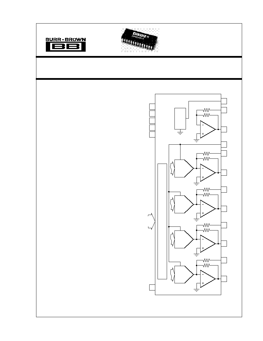
A
20k
20k
20k
20k
10k
10k
Logic
4
3
11
5
1
9
14
28
15
7
12
17
+V Out
REF
Inv In
Inv Out
BPO B
V B
OUT
BPO C
V C
OUT
+V
L
+V
S
≠V
S
AGND
DGND
10V
Ref
DAC B
DAC C
DAC4814
5
A
2
A
3
20k
20k
8
13
BPO D
V D
OUT
DAC D
A
4
20k
20k
10
6
2
V In
REF
BPO A
V A
OUT
DAC A
A
1
Serial
Data and
Control In
Serial
Data
Out
18
DAC4814
Quad 12-Bit Digital-to-Analog Converter
(Serial Interface)
International Airport Industrial Park ∑ Mailing Address: PO Box 11400 ∑ Tucson, AZ 85734 ∑ Street Address: 6730 S. Tucson Blvd. ∑ Tucson, AZ 85706
Tel: (520) 746-1111 ∑ Twx: 910-952-1111 ∑ Cable: BBRCORP ∑ Telex: 066-6491 ∑ FAX: (520) 889-1510 ∑ Immediate Product Info: (800) 548-6132
Æ
© 1991 Burr-Brown Corporation
PDS-1111B
Printed in U.S.A. April, 1995

2
Æ
DAC4814
SPECIFICATIONS
, Guaranteed over T
A
= ≠40
∞
C to +85
∞
C unless otherwise specified.
ELECTRICAL
Specifications as shown for V
S
=
±
12V or
±
15V, V
L
= +5V, and R
L
= 2k
unless otherwise noted.
DAC4814AP
DAC4814BP
PARAMETER
CONDITIONS
MIN
TYP
MAX
MIN
TYP
MAX
UNITS
DIGITAL INPUTS
Resolution
12
*
Bits
V
IH
(Input High Voltage)
+2
+5
*
*
V
V
IL
(Input Low Voltage)
0
+0.8
*
*
V
I
IN
( Input Current)
T
A
= 25
∞
C
±
1
*
µ
A
T
A
= ≠40
∞
C to +85
∞
C
±
10
*
µ
A
C
IN
(Input Capacitance)
0.8
*
pF
DIGITAL OUTPUT
Data Out V
OL
I
SINK
= 1.6mA
0
+0.4
*
*
V
V
OH
I
SOURCE
= 500
µ
A
+2.4
+5
*
*
V
ACCURACY
Integral, Relative Linearity
(1)
±
1
±
1/2
LSB
Differential Nonlinearity
(2)
T
A
= 25
∞
C
±
1
*
LSB
T
A
= ≠40
∞
C to +85
∞
C
+1.5/≠1
±
1
LSB
Unipolar Offset Error
T
A
= +25
∞
C
±
1
±
0.5
mV
T
A
= ≠40
∞
C to +85
∞
C
±
3
*
mV
Bipolar Zero Error
±
20
±
10
mV
Gain Error Unipolar, Bipolar
With Internal or External 10.0V Ref
±
0.2
±
0.15
%
Power Supply Sensitivity
(3)
V
S
=
±
11.4V to
±
18V
30
*
ppmFSR/V
V
L
= +4.5V to +5.5V
TEMPERATURE DRIFT
Gain Drift Unipolar, Bipolar
±
5
±
30
*
±
20
ppm/
∞
C
Unipolar Offset Drift
±
0.1
±
5
*
*
ppmFSR/
∞
C
Bipolar Zero Drift
±
5
±
15
*
±
8
ppmFSR/
∞
C
REFERENCE OUTPUT
Output Voltage
+9.980
+10
+10.020
+9.985
*
+10.015
V
Reference Drift
±
2
±
30
*
±
20
ppm/
∞
C
Output Current
T
A
= 25
∞
C
+10/≠5
*
mA
T
A
= ≠40
∞
C to +85
∞
C
+6.5/≠5
*
mA
Max Load Capacitance (For Stability)
500
*
pF
Short Circuit Current
±
20
*
mA
Load Regulation
40
*
ppm/mA
(
V
OUT
vs
I
LOAD
)
Supply Regulation
±
5
*
ppm/V
(
V
OUT
vs
V
S
)
INVERTER
≠10V Reference
(4)
, Inverter Output
≠10.020
≠10
≠9.980
≠10.015
*
≠9.985
V
≠10V Reference Drift
±
30
±
20
ppm/
∞
C
DC Output Impedance
0.1
*
Output Current
±
7
*
mA
Max Load Capacitance (For Stability)
200
*
pF
Short Circuit Current
±
30
*
mA
REFERENCE INPUT
Reference Input Resistance
1.75
2.5
*
*
k
Inverter Input Resistance
7
10
*
*
k
BPO Input Resistance
14
20
*
*
k
Reference Input Range
±
10
*
V
ANALOG SIGNAL OUTPUTS
Voltage Range
≠V
S
+ 1.4
+V
S
≠ 1.4
*
*
V
DC Output Impedance
0.1
*
Output Current
±
5
*
mA
Max Load Capacitance (For Stability)
V
OUT
500
*
pF
Short Circuit Current
±
30
*
mA
DYNAMIC PERFORMANCE
(5)
C
L
= 100pF
Unipolar Mode Settling Time
To 1/2 LSB of Full Scale
2.5
10
*
*
µ
s
Bipolar Mode Settling Time
To 1/2 LSB of Full Scale
3.5
10
*
*
µ
s
Slew Rate
10
*
V/
µ
s
Small-Signal Bandwidth
3
*
MHz
ANALOG GROUND CURRENT
(Code Dependent)
±
4
*
mA
DIGITAL CROSSTALK
Full Scale Transition
3
*
nV-s
C
L
= 100pF
D/A GLITCH IMPULSE
30
*
nV-s
3
Æ
DAC4814
NOTES: (1) End point linearity. (2) Guaranteed monotonic. (3) Change in bipolar full scale output. Includes voltage output DAC, voltage reference, and reference
inverter. (4) Inverter output with inverter input connected to +V
REF
. (5) Guaranteed to but not tested.
The information provided herein is believed to be reliable; however, BURR-BROWN assumes no responsibility for inaccuracies or omissions. BURR-BROWN assumes
no responsibility for the use of this information, and all use of such information shall be entirely at the user's own risk. Prices and specifications are subject to change
without notice. No patent rights or licenses to any of the circuits described herein are implied or granted to any third party. BURR-BROWN does not authorize or warrant
any BURR-BROWN product for use in life support devices and/or systems.
ABSOLUTE MAXIMUM RATINGS
+V
L
to AGND ................................................................................. 0V, +7V
+V
L
to DGND ................................................................................ 0V, +7V
+V
S
to AGND .............................................................................. 0V, +18V
≠V
S
to AGND ............................................................................... 0V,≠18V
AGND to DGND ................................................................................
±
0.3V
Any digital input to DGND .............................................. ≠0.3V, +V
L
+0.3V
Ref In to AGND ..................................................................................
±
25V
Ref In to DGND ..................................................................................
±
25V
Storage Temperature Range .......................................... ≠55
∞
C to +125
∞
C
Operating Temperature Range ......................................... ≠40
∞
C to +85
∞
C
Lead Temperature (soldering, 10s) ................................................ +300
∞
C
Junction Temperature .................................................................... +155
∞
C
Output Short Circuit ................................... Continuous to common or
±
V
S
Reference Short Circuit .............................. Continuous to common or +V
S
ELECTROSTATIC
DISCHARGE SENSITIVITY
Electrostatic discharge can cause damage ranging from
performance degradation to complete device failure. Burr-
Brown Corporation recommends that all integrated circuits be
handled and stored using appropriate ESD protection
methods.
PACKAGE INFORMATION
PACKAGE DRAWING
MODEL
PACKAGE
NUMBER
(1)
DAC4814AP
28-Pin Plastic DBL Wide DIP
215
DAC4814BP
28-Pin Plastic DBL Wide DIP
215
NOTE: (1) For detailed drawing and dimension table, please see end of data
sheet, or Appendix D of Burr-Brown IC Data Book.
POWER SUPPLY
+V
S
and ≠V
S
±
11.4
±
15
±
18
*
*
*
V
+V
L
4.5
5
5.5
*
*
*
V
+I
S
+20
+24
*
*
mA
≠I
S
≠20
≠25.5
*
*
mA
+I
L
Digital Inputs = 0V or +V
L
0.4
2
*
*
mA
+I
L
Digital Inputs = V
IL
or V
IH
10
*
mA
Total Power, All DACs
600
753
*
*
mW
TEMPERATURE RANGE
Specified
≠40
+85
*
*
∞
C
Operating
≠40
+85
*
*
∞
C
Thermal Resistance,
JA
75
*
∞
C/W
SPECIFICATIONS
(CONT)
, Guaranteed over T
A
= ≠40
∞
C to +85
∞
C unless otherwise specified.
ELECTRICAL
Specifications as shown for V
S
=
±
12V or
±
15V, V
L
= +5V, and R
L
= 2k
unless otherwise noted.
DAC4814AP
DAC4814BP
PARAMETER
CONDITIONS
MIN
TYP
MAX
MIN
TYP
MAX
UNITS

4
Æ
DAC4814
PIN DESIGNATIONS
PIN
DESCRIPTOR
FUNCTION
PIN
DESCRIPTOR
FUNCTION
1
V
OUT
B
Analog output voltage, DAC B
28
+V
L
Positive logic power supply, +5V input
2
V
OUT
A
Analog output voltage, DAC A
27
LATCH A
Latch data update, logic input, DAC A
3
Inv In
Inverter (A
5
) input
26
LATCH B
Latch data update, logic input, DAC B
4
+V
REF
Out
Positive reference voltage output (+10V output)
25
MODE
Selection input for unipolar or bipolar reset to zero
5
BPO B
Biplolar offset input, DAC B
24
CLR
Asynchronous input reset to zero
6
BPO A
Bipolar offset input, DAC A
23
CS
Chip select enable, DAC A, B, C, and D
7
≠V
S
Negative analog power supply , ≠15V input
22
Data In
Serial data input
8
BPO D
Bipolar offset input, DAC D
21
LATCH C
Latch data update, logic input, DAC C
9
BPO C
Bipolar offset input, DAC C
20
LATCH D
Latch data update, logic input, DAC D
10
V
REF
In
±
Reference voltage input
19
CLK
Clock input
11
Inv Out
Inverter (A
5
) output
18
Data Out
Serial data output
12
AGND
Analog common
17
DGND
Digital common
13
V
OUT
D
Analog output voltage, DAC D
16
NC
No internal connection
14
V
OUT
C
Analog output voltage, DAC C
15
+V
S
Positive analog power supply, +15V input
TYPICAL PERFORMANCE CURVES
T
A
= +25
∞
C, V
S
=
±
12V or
±
15V, V
L
= +5V unless otherwise noted.
PIN CONFIGURATION
TOP VIEW
+V
L
LATCH A
LATCH B
MODE
CLR
CS
Data In
LATCH C
LATCH D
CLK
Data Out
DGND
NC
+V
S
1
2
3
4
5
6
7
8
9
10
11
12
13
14
28
27
26
25
24
23
22
21
20
19
18
17
16
15
V
OUT
B
V
OUT
A
Inv In
+V
REF
Out
BPO B
BPO A
≠V
S
BPO D
BPO C
V
REF
In
Inv Out
AGND
V
OUT
D
V
OUT
C
DAC4814
NC = No Internal Connection
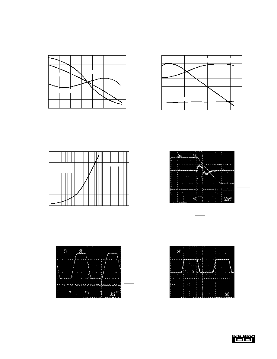
PSRR vs FREQUENCY (Bipolar Mode)
80
70
60
50
40
30
20
10
0
PSRR (dB)
1k
10k
100k
1M
Frequency (Hz)
V
OUT
= +10V
V
OUT
= 0V
NOISE vs BANDWIDTH (Bipolar Mode)
250
200
150
100
50
0
Voltage Noise (µVrms)
100
1k
10k
100k
1M
Frequency (Hz)
V
OUT
= +10V
FFF
HEX
V
OUT
= 0V
800
HEX
5
Æ
DAC4814
TYPICAL PERFORMANCE CURVES
(CONT)
T
A
= +25
∞
C, V
S
=
±
12V or
±
15V, V
L
= +5V unless otherwise noted.
V
OUT
LATCH
V
OUT
B
V
OUT
A
LATCH A
NOTE: Crosstalk is dominated by digital crosstalk/
feedthrough of the LATCH signal.
V
OUT
0V
+5V
0V
CROSSTALK (Bipolar Mode)
Time (500ns/div)
V
OUT
0V
FULL-SCALE OUTPUT SWING
UNIPOLAR (10V Step)
Time (2µs/div)
V
OUT
(5V/div)
FULL-SCALE OUTPUT SWING
BIPOLAR (20V Step)
Time (2µs/div)
V
OUT
(5V/div)
+5V
0V
0V
OUTPUT VOLTAGE SWING vs RESISTOR LOAD
Load Resistance ( )
25
20
15
10
5
0
V
OUT
(Vp-p)
10
100
1K
10K
V
S
= ±15V
V
L
= 5V
10V REF
POWER SUPPLY CURRENT vs TEMPERATURE
21.8
21.5
21.2
20.9
20.6
20.3
20
19.4
±I
S
(mA) Analog Supply
≠40
≠20
0
20
40
60
80
Temperature (∞C)
+I
L
(mA) Logic Supply
2.8
2.4
2
1.6
1.2
0.8
0.4
0
+I
L
(All Logic Inputs = 2V)
I
S
+I
L
(All Logic Inputs = 0V or V
L
)
CHANGE OF GAIN, BIPOLAR OFFSET AND ZERO ERROR
vs TEMPERATURE
1.5E+00
1.0E+00
5.0E+00
0.0E+00
≠5.0E≠01
≠1.0E+00
≠1.5E+00
Bipolar Offset and Zero Error (mV)
≠40
≠20
0
20
40
60
+80
Temperature (∞C)
1.5E≠02
1.0E≠02
5.0E≠03
0.0E+00
≠5.0E≠03
≠1.0E≠02
≠1.5E≠02
Gain Error (%)
100
Bipolar Offset
Gain Error
Bipolar Zero