 | –≠–ª–µ–∫—Ç—Ä–æ–Ω–Ω—ã–π –∫–æ–º–ø–æ–Ω–µ–Ω—Ç: DAC709 | –°–∫–∞—á–∞—Ç—å:  PDF PDF  ZIP ZIP |

Microprocessor-Compatible
16-BIT DIGITAL-TO-ANALOG CONVERTERS
FEATURES
q
TWO-CHIP CONSTRUCTION
q
HIGH-SPEED 16-BIT PARALLEL, 8-BIT
(BYTE) PARALLEL, AND SERIAL INPUT
MODES
q
DOUBLE-BUFFERED INPUT REGISTER
CONFIGURATION
q
V
OUT
AND I
OUT
MODELS
q
HIGH ACCURACY:
Linearity Error
±
0.003% of FSR max
Differential Linearity Error
±
0.006% of FSR
max
q
MONOTONIC (TO 14 BITS) OVER
SPECIFIED TEMPERATURE RANGE
q
HERMETICALLY SEALED
q
LOW COST PLASTIC VERSIONS
AVAILABLE (DAC707JP/KP)
DESCRIPTION
The DAC708 and DAC709 are 16-bit converters de-
signed to interface to an 8-bit microprocessor bus. 16-
bit data is loaded in two successive 8-bit bytes into
parallel 8-bit latches before being transferred into the
D/A latch. The DAC708 and DAC709 are current and
voltage output models respectively and are in 24-pin
hermetic DIPs. Input coding is Binary Two's Comple-
ment (bipolar) or Unipolar Straight Binary (unipolar,
when an external logic inverter is used to invert the
MSB). In addition, the DAC708/709 can be loaded
serially (MSB first).
The DAC707 is designed to interface to a 16-bit bus.
Data is written into a 16-bit latch and subsequently the
D/A latch. The DAC707 has bipolar voltage output
and input coding is Binary Two's Complement (BTC).
All models have Write and Clear control lines as well
as input latch enable lines. In addition, DAC708 and
DAC709 have Chip Select control lines. In the bipolar
mode, the Clear input sets the D/A latch to give zero
voltage or current output. They are all 14-bit accurate
and are complete with reference, and for the DAC707,
and DAC709, a voltage output amplifier. All models
are available with an optional burn-in screening.
DAC707/708/709 Block Diagram
High
Byte
Latch
Latch Enables/
Mode Select
Control
Logic
CLEAR
WRITE
CHIP SELECT
16-Bit
D/A
Con-
verter
DAC707 or DAC709
Only
Summing Junction (708, 709)
10V Range (708, 709)
V
OUT
Reference
Circuit
Bipolar
Offset
Low
Byte
Latch
D/A
Latch
Serial
(DAC708, 709)
8-Bit
(DAC708, 709)
or
16-Bit (DAC707)
Serial
Data
PDS-557H
Æ
International Airport Industrial Park ∑ Mailing Address: PO Box 11400, Tucson, AZ 85734 ∑ Street Address: 6730 S. Tucson Blvd., Tucson, AZ 85706 ∑ Tel: (520) 746-1111 ∑ Twx: 910-952-1111
Internet: http://www.burr-brown.com/ ∑ FAXLine: (800) 548-6133 (US/Canada Only) ∑ Cable: BBRCORP ∑ Telex: 066-6491 ∑ FAX: (520) 889-1510 ∑ Immediate Product Info: (800) 548-6132
DAC707
DAC708
DAC709

Æ
DAC707/708/709
2
SPECIFICATIONS
ELECTRICAL
At T
A
= +25
∞
C, V
CC
=
±
15V, V
DD
= +5V, and after a 10-minute warm-up, unless otherwise noted.
DAC707/708/709KH,
DAC707/708/
DAC707JP
DAC707KP
709BH, SH
PRODUCT
MIN
TYP
MAX
MIN
TYP
MAX
MIN
TYP
MAX
UNITS
INPUT
DIGITAL INPUT
Resolution
16
*
*
Bits
Bipolar Input Code (all models)
Binary Two's Complement
*
*
Unipolar Input Code
(1)
(DAC708/709 only)
Unipolar Straight Binary
*
Logic Levels
(2)
: V
IH
+2.0
+5.5
*
*
*
*
V
V
IL
≠1.0
+0.8
*
*
*
*
V
I
IH
(V
I
= +2.7V)
1
*
*
µ
A
I
IL
(V
I
= +0.4V)
1
*
*
µ
A
TRANSFER CHARACTERISTICS
ACCURACY
(3)
Linearity Error
±
0.003
±
0.006
±
0.0015
±
0.003
*
*
% of FSR
(4)
Differential Linearity Error
(5)
±
0.0045
±
0.012
±
0.003
±
0.006
*
*
% of FSR
at Bipolar Zero
(5, 6)
±
0.003
±
0.006
±
0.0015
±
0.003
% of FSR
Gain Error
(7)
±
0.07
±
0.30
*
±
0.15
±
0.05
±
0.10
%
Zero Error
(7)
±
0.05
±
0.1
*
*
*
*
% of FSR
Monotonicity Over Spec Temp Range
13
14
14
Bits
Power Supply Sensitivity: +V
CC,
≠V
CC
±
0.0015
±
0.006
*
*
*
±
0.003
% of FSR/%V
CC
V
DD
±
0.0001
±
0.001
*
*
*
*
% of FSR/%V
DD
DRIFT (Over Spec Temp Range
(3)
)
Total Error Over Temp Range
(8)
±
0.08
*
±
0.15
*
±
0.10
% of FSR
Total Full Scale Drift
±
10
*
±
25
*
±
15
ppm of FSR/
∞
C
Gain Drift
±
10
±
30
*
±
25
±
7
±
15
ppm/
∞
C
Zero Drift: Unipolar (DAC708/709 only)
±
2.5
±
5
±
1.5
±
3
ppm of FSR/
∞
C
Bipolar (all models)
±
5
±
15
*
±
12
±
4
±
10
ppm of FSR/
∞
C
Differential Linearity Over Temp
(5)
±
0.012
+0.009,
*
≠0.006
% of FSR
Linearity Error Over Temp
(5)
±
0.012
±
0.006
*
% of FSR
SETTLING TIME (to
±
0.003% of FSR)
(9)
Voltage Output Models
Full Scale Step (2k
load)
4
*
8
*
8
µ
s
1LSB Step at Worst Case Code
(10)
2.5
*
4
*
4
µ
s
Slew Rate
10
*
*
V/
µ
s
Current Output Models
Full Scale Step (2mA): 10 to 100
Load
350
*
ns
1k
Load
1
*
µ
s
OUTPUT
VOLTAGE OUTPUT MODELS
Output Voltage Range
DAC709: Unipolar (USB Code)
0 to +10
*
V
Bipolar (BTC Code)
±
5,
±
10
*
V
DAC707 Bipolar (BTC Code)
±
10
*
*
V
Output Current
±
5
*
*
mA
Output Impedance
0.15
*
*
Short Circuit to Common Duration
Indefinite
*
*
CURRENT OUTPUT MODELS
Output Current Range (
±
30% typ)
DAC708: Unipolar (USB Code)
0 to ≠2
*
mA
Bipolar (BTC Code)
±
1
*
mA
Unipolar Output Impedance (
±
30% typ)
4.0
*
k
Bipolar Output Impedance (
±
30% typ)
2.45
*
k
Compliance Voltage
±
2.5
*
V
The information provided herein is believed to be reliable; however, BURR-BROWN assumes no responsibility for inaccuracies or omissions. BURR-BROWN assumes
no responsibility for the use of this information, and all use of such information shall be entirely at the user's own risk. Prices and specifications are subject to change
without notice. No patent rights or licenses to any of the circuits described herein are implied or granted to any third party. BURR-BROWN does not authorize or warrant
any BURR-BROWN product for use in life support devices and/or systems.
3
Æ
DAC707/708/709
PACKAGE DRAWING
PRODUCT
PACKAGE
NUMBER
(1)
DAC707JP
28-Pin Plastic DBL Wide DIP
215
DAC707KP
28-Pin Plastic DBL Wide DIP
215
DAC707BH
28LD Side Brazed
149
Hermetic Dip
DAC707KH
28LD Side Brazed
149
Hermetic DIP
DAC707SH
28LD Side Brazed
149
Hermetic DIP
DAC708BH
24LD Side Brazed
165
Hermetic DIP
DAC708KH
24LD Side Brazed
165
Hermetic DIP
DAC708SH
24LD Side Brazed
165
Hermetic DIP
DAC709BH
24LD Side Brazed
165
Hermetic DIP
DAC709KH
24LD Side Brazed
165
Hermetic DIP
DAC709SH
24LD Side Brazed
165
Hermetic DIP
NOTE: (1) For detailed drawing and dimension table, please see end of data
sheet, or Appendix C of Burr-Brown IC Data Book.
DAC707/708/709KH,
DAC707/708/
DAC707JP
DAC707KP
709BH, SH
PRODUCT
MIN
TYP
MAX
MIN
TYP
MAX
MIN
TYP
MAX
UNITS
At T
A
= +25
∞
C, V
CC
=
±
15V, V
DD
= +5V, and after a 10-minute warm-up, unless otherwise noted.
ELECTRICAL (CONT)
*Specification same as for models in column to the left.
NOTES: (1) MSB must be inverted externally prior to DAC708/709 input. (2) Digital inputs are TTL, LSTTL, 54/74C, 54/74HC and 54/74HTC compatible over the specified
temperature range. (3) DAC708 (current-output models) are specified and tested with an external output operational amplifier connected using the internal feedback
resistor in all tests. (4) FSR means Full Scale Range. For example, for
±
10V output, FSR = 20V. (5)
±
0.0015% of Full Scale Range is equal to 1 LSB in 16-bit resolution,
±
0.003% of Full Scale Range is equal to 1 LSB in 15-bit resolution.
±
0.006% of Full Scale Range is equal to 1 LSB in 14-bit resolution. (6) Error at input code 0000
H
.
(For unipolar connection on DAC708/709, the MSB must be inverted externally prior to D/A input.) (7) Adjustable to zero with external trim potentiometer. Adjusting the
gain potentiometer rotates the transfer function around the bipolar zero point. (8) With gain and zero errors adjusted to zero at +25
∞
C. (9) Maximum represents the 3
limit. Not 100% tested for this parameter. (10) The bipolar worst-case code change is FFFF
H
to 0000
H
and 0000
H
to FFFF
H
. For unipolar (DAC708/709 only) it is 7FFF
H
to 8000
H
and 8000
H
to 7FFF
H
.
POWER SUPPLY REQUIREMENTS
Voltage (all models): +V
CC
+13.5
+15
+16.5
*
*
*
*
*
*
V
≠V
CC
≠13.5
≠15
≠16.5
*
*
*
*
*
*
V
V
DD
+4.5
+5
+5.5
*
*
*
*
*
*
V
Current (No Load, +15V Supplies)
Current Output Models: +V
CC
+10
+25
*
*
mA
≠V
CC
≠13
≠25
*
*
mA
V
DD
+5
+10
*
*
mA
Voltage Output Models: +V
CC
+16
+30
*
*
*
*
mA
≠V
CC
≠18
≠30
*
*
*
*
mA
V
DD
+5
+10
*
*
*
*
mA
Power Dissipation (
±
15V supplies)
Current Output Models
370
800
*
*
mW
Voltage Output Models
535
*
950
*
*
mW
TEMPERATURE RANGE
Specification: BH Grades
≠25
+85
∞
C
JP, KP, KH Grades
0
+70
*
*
∞
C
SH Grades
≠55
+125
∞
C
Storage: Ceramic
≠65
+150
≠65
+150
∞
C
Plastic
≠60
+100
*
*
∞
C
PACKAGE INFORMATION
ABSOLUTE MAXIMUM RATINGS
V
DD
to COMMON ........................................................................ 0V, +15V
+V
CC
to COMMON ..................................................................... 0V, +18V
≠V
CC
to COMMON ...................................................................... 0V, ≠18V
Digital Data Inputs to COMMON ..................................... ≠0.5V, V
DD
+0.5
DC Current any input .....................................................................
±
10mA
Reference Out to COMMON ...................... Indefinite Short to COMMON
V
OUT
(DAC707, DAC709) ........................... Indefinite Short to COMMON
External Voltage Applied to R
F
(pin 13 or 14, DAC708) ..................
±
18V
External Voltage Applied to D/A Output
(pin 1, DAC707; pin 14, DAC709) .........................................................
±
5V
Power Dissipation ........................................................................ 1000mW
Storage Temperature ..................................................... ≠60
∞
C to +150
∞
C
Lead Temperature (soldering, 10s) ................................................. 300
∞
C
Stresses above those listed under "Absolute Maximum Ratings" may
cause permanent damage to the device. Exposure to absolute maximum
conditions for extended periods may affect device reliability.
ELECTROSTATIC
DISCHARGE SENSITIVITY
This integrated circuit can be damaged by ESD. Burr-Brown
recommends that all integrated circuits be handled with
appropriate precautions. Failure to observe proper handling
and installation procedures can cause damage.
ESD damage can range from subtle performance degradation
to complete device failure. Precision integrated circuits may
be more susceptible to damage because very small parametric
changes could cause the device not to meet its published
specifications.

Æ
DAC707/708/709
4
CONNECTION DIAGRAMS
F2
OUT
A
A
A
D7 (D15)
D6 (D14)
D5 (D13)
D4 (D12)
D3 (D11)
D2 (D10)
D1 (D9)
D0 (D8)/S1
DCOM
24
23
22
21
20
19
18
17
16
15
14
13
28
27
26
25
24
23
22
21
20
19
18
17
16
15
1
2
3
4
5
6
7
8
9
10
11
12
1
2
3
4
5
6
7
8
9
10
11
12
13
14
V
CS
WR
CLR
≠V
+V
GA
BPO
SJ
ACOM
V
R
DD
CC
F
CC
DD
V
+
(2)
(2)
(2)
(3)
+
+
CC
CC
≠V
+V
(1)
(1)
3.9M
270k
Offset Adjust
Gain
Adjust
Control
Lines
Connect for bipolar operation.
Connect for 10V range.
Leave pin 13 open for 20V range.
+
10k
DAC709
Only
16-Bit
Ladder
Resistor
Network
and
Current
Switches
Reference
Circuit
D/A
Latch
Low
Byte
Latch
High
Byte
Latch
2
0
1
D0 (LSB)
D1
D2
D3
D4
D5
D6
D7
D8
D9
D10
D11
D12
D13
R
16-Bit
Ladder
Resistor
Network
and
Current
Switches
D/A Latch
Input Latch
Digital
Inputs
V
+V
≠V
V
CLR
WR
A
A
0
1
(2)
(3)
(1)
3.9M
270k
NOTES: (1) Potentiometers are 10k to 100k .
(2) Decoupling capcitors are 0.1µF to 1.0µF.
(3) Bypass, 0.0022µF to 0.01µF.
DD
CC
≠V
CC
+V
(2)
Digital Inputs
Latch Enable Lines
Control Lines
Gain Adjust
Analog Common
CC
Offset
Adjust
Digital
Common
(2)
V
DD
OUT
NOTES: (1) Potentiometer is
10k to 100k . (2) Decoupling
capcitors are 0.1µF to 1.0µF.
DAC708/709
DAC707
Register
Enable
Lines
Data
Inputs
DCOM
ACOM
SJ
GA
(MSB) D15
D14
10k
CC
ORDERING INFORMATION
TEMPERATURE
INPUT
OUTPUT
PRODUCT
RANGE
CONFIGURATION
CONFIGURATION
DAC707JP
0
∞
C to +70
∞
C
16-bit port
±
10V output
DAC707JP-BI
(1)
0
∞
C to +70
∞
C
16-bit port
±
10V output
DAC707KP
0
∞
C to +70
∞
C
16-bit port
±
10V output
DAC707KP-BI
(1)
0
∞
C to +70
∞
C
16-bit port
±
10V output
DAC707KH
0
∞
C to +70
∞
C
16-bit port
±
10V output
DAC707KH-BI
(1)
0
∞
C to +70
∞
C
16-bit port
±
10V output
DAC707BH
≠25
∞
C to +85
∞
C
16-bit port
±
10V output
DAC707BH-BI
(1)
≠25
∞
C to +85
∞
C
16-bit port
±
10V output
DAC707SH
≠55
∞
C to +125
∞
C
16-bit port
±
10V output
DAC707SH-BI
(1)
≠55
∞
C to +125
∞
C
16-bit port
±
10V output
DAC708KH
0
∞
C to +70
∞
C
8-bit port
±
1mA output
DAC708BH
≠25
∞
C to +85
∞
C
8-bit port
±
1mA output
DAC708SH
≠55
∞
C to +125
∞
C
8-bit port
±
1mA output
DAC709KH
0
∞
C to +70
∞
C
8-bit port
±
10V output
DAC709BH
≠25
∞
C to +85
∞
C
8-bit port
±
10V output
DAC709SH
≠55
∞
C to +125
∞
C
8-bit port
±
10V output
NOTE: (1) 25 piece minimum order.

5
Æ
DAC707/708/709
DESCRIPTION OF PIN FUNCTIONS
DAC707
Pin
DAC708/709
DESIGNATOR
DESCRIPTION
#
DESIGNATOR
DESCRIPTION
V
OUT
Voltage output for DAC707 (
±
10V)
1
A
2
Latch enable for D/A latch (Active low)
V
DD
Logic supply (+5V)
2
A
0
Latch enable for "low byte" input (Active low). When
both A
0
and A
1
are logic "0", the serial input mode is
selected and the serial input is enabled.
DCOM
Digital common
3
A
1
Latch enable for "high byte" input (Active low). When
both A
0
and A
1
are logic "0", the serial input mode is
selected and the serial input is enabled.
ACOM
Analog common
4
D7 (D15)
Input for data bit 7 if enabling low byte (LB) latch or
data bit 15 if enabling the high byte (HB) latch.
SJ
Summing junction of the internal output op amp for the
5
D6 (D14)
Input for data bit 6 if enabling LB latch or data bit 14 if
DAC707. Offset adjust circuit is connected to the
enabling the HB latch.
summing junction of the output amplifier. Refer to Block
Diagram.
GA
Gain adjust pin. Refer to Connection Diagram for gain
6
D5 (D13)
Data bit 5 (LB) or data bit 13 (HB)
adjust circuit.
+V
CC
Positive supply voltage (+15V)
7
D4 (D12)
Data bit 4 (LB) or data bit 12 (HB)
≠V
CC
Negative supply voltage (≠15V)
8
D3 (D11)
Data bit 3 (LB) or data bit 11 (HB)
CLR
Clear line. Sets the input latch to zero and sets the D/A
9
D2 (D10)
Data bit 2 (LB) or data bit 10 (HB)
latch to the input code that gives bipolar zero on the
D/A output (Active low)
WR
Write control line (Active low)
10
D1 (D9)
Data bit 1 (LB) or data bit 9 (HB)
A
1
Enable for D/A converter latch (Active low)
11
D0 (D8)/SI
Data bit 0 (LB) or data bit 8 (HB). Serial input when
serial mode is selected.
A
0
Enable for input latch (Active low)
12
DCOM
Digital common
D15 (MSB)
Data bit 15 (Most Significant Bit)
13
R
F2
Feedback resistor for internal or external operational
amplifier. Connect to pin 14 when a 10V output range
is desired. Leave open for a 20V output range.
D14
Data bit 14
14
V
OUT
Voltage output for DAC709 or feedback resistor for
R
F1
(DAC708)
use with an external output op amp for the DAC708.
Refer to Connection Diagram for connection of
external op amp to DAC708.
D13
Data bit 13
15
ACOM
Analog common
D12
Data bit 12
16
SJ (DAC709)
Summing junction of the internal output op amp for the
I
OUT
(DAC708)
DAC709, or the current output for the DAC708. Refer
to Connection Diagram for connection of external op
amp to DAC708.
D11
Data bit 11
17
BPO
Bipolar offset. Connect to pin 16 when operating in the
bipolar mode. Leave open for unipolar mode.
D10
Data bit 10
18
GA
Gain adjust pin
D9
Data bit 9
19
+V
CC
Positive supply voltage (+15V)
D8
Data bit 8
20
≠V
CC
Negative supply voltage (≠15V)
D7
Data bit 7
21
CLR
Clear line. Sets the high and low byte input registers
to zero and, for bipolar operation, sets the D/A register
to the input code that gives bipolar zero on the D/A
output. (In the unipolar mode, invert the MSB prior to
the D/A.)
D6
Data bit 6
22
WR
Write control line
D5
Data bit 5
23
CS
Chip select control line
D4
Data bit 4
24
V
DD
Logic supply (+5V)
D3
Data bit 3
25
No pin
D2
Data bit 2
26
No pin
(The DAC708 and DAC709 are in 24-pin packages)
D1
Data bit 1
27
No pin
D0 (LSB)
Data bit 0 (Least Significant Bit)
28
No pin
Æ
DAC707/708/709
6
DISCUSSION OF
SPECIFICATIONS
DIGITAL INPUT CODES
For bipolar operation, the DAC707/708/709 accept positive-
true binary two's complement input code. For unipolar
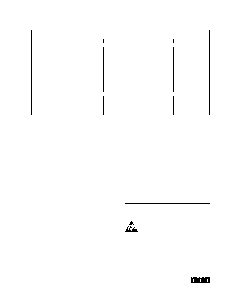
operation (DAC708/709 only) the input code is positive-true
straight-binary provided that the MSB input is inverted with
an external inverter. See Table I.
the MSB must be inverted). This code corresponds to zero
volts (DAC707 and DAC709) or zero milliamps (DAC708)
at the analog output. The maximum change in offset at t
MIN
or t
MAX
is referenced to the zero error at +25
∞
C and is divided
by the temperature change. This drift is expressed in FSR/
∞
C.
SETTLING TIME
Settling time of the D/A is the total time required for the
analog output to settle within an error band around its final
value after a change in digital input. Refer to Figure 1 for
typical values for this family of products.
FIGURE 1. Final-Value Error Band Versus Full-Scale Range
Settling Time.
Voltage Output
Settling times are specified to
±
0.003% of FSR (
±
1/2LSB
for 14 bits) for two input conditions: a full-scale range
change of 20V (
±
10V) or 10V (
±
5V or 0 to 10V) and a 1LSB
change at the "major carry", the point at which the worst-
case settling time occurs. (This is the worst-case point since
all of the input bits change when going from one code to the
next.)
Current Output
Settling times are specified to
±
0.003% of FSR for a full-
scale range change for two output load conditions: one for
10
to 100
and one for 1000
. It is specified this way
because the output RC time constant becomes the dominant
factor in determining settling time for large resistive loads.
COMPLIANCE VOLTAGE
Compliance voltage applies only to current output models. It
is the maximum voltage swing allowed on the output current
pin while still being able to maintain specified accuracy.
POWER SUPPLY SENSITIVITY
Power supply sensitivity is a measure of the effect of a
change in a power supply voltage on the D/A converter
ANALOG OUTPUT
Digital
Unipolar Straight Binary
(1)
Binary Two's Complement
Input
(DAC708/709 only; connected
(Bipolar operation;
Codes
for Unipolar operation)
all models)
7FFF
H
+1/2 Full Scale ≠1LSB
(2)
+Full Scale
0000
H
Zero
Zero
FFFF
H
+Full Scale
≠1LSB
8000
H
+1/2 Full Scale
≠Full Scale
NOTES: (1) MSB must be inverted externally. (2) Assumes MSB is inverted
externally.
TABLE I. Digital Input Codes.
ACCURACY
Linearity
This specification describes one of the most important mea-
sures of performance of a D/A converter. Linearity error is
the deviation of the analog output from a straight line drawn
through the end points (≠Full Scale point and +Full Scale
point).
Differential Linearity Error
Differential Linearity Error (DLE) of a D/A converter is the
deviation from an ideal 1LSB change in the output when the
input changes from one adjacent code to the next. A differ-
ential linearity error specification of
±
1/2LSB means that the
output step size can be between 1/2LSB and 3/2LSB when
the input changes between adjacent codes. A negative DLE
specification of ≠1LSB maximum (≠0.006% for 14-bit reso-
lution) insures monotonicity.
Monotonicity
Monotonicity assures that the analog output will increase or
remain the same for increasing input digital codes. The
DAC707/708/709 are specified to be monotonic to 14 bits
over the entire specification temperature range.
DRIFT
Gain Drift
Gain Drift is a measure of the change in the full-scale range
output over temperature expressed in parts per million per
degree centigrade (ppm/
∞
C). Gain drift is established by: (1)
testing the end point differences at t
MIN
, +25
∞
C and t
MAX
; (2)
calculating the gain error with respect to the +25
∞
C value;
and (3) dividing by the temperature change.
Zero Drift
Zero Drift is a measure of the change in the output with
0000
H
applied to the D/A converter inputs over the specified
temperature range. (For the DAC708/709 in unipolar mode,
1
0.1
0.01
0.01
0.1
1
10
Settling Time (µs)
Final-Value Error Band
Percent of Full-Scale Range (±% of FSR) 0.001
DAC707
DAC709
R = 100
R = 1k
L
L
DAC708
7
Æ
DAC707/708/709
output. It is defined as a percent of FSR change in the output
per percent of change in either the positive supply (+V
CC
),
negative supply (≠V
CC
) or logic supply (V
DD
) about the
nominal power supply voltages (see Figure 2). It is specified
for DC or low frequency changes. The typical performance
curve in Figure 2 shows the effect of high frequency changes
in power supply voltages.
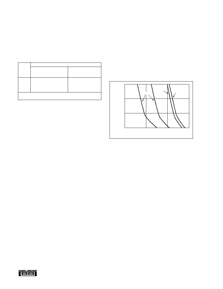
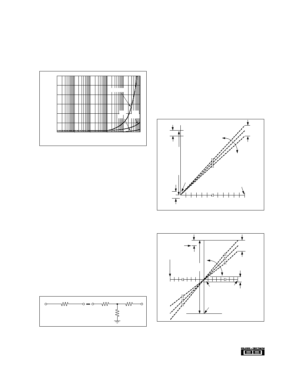
Zero Adjustment
For unipolar (USB) configurations, apply the digital input
code that produces zero voltage or zero current output and
adjust the zero potentiometer for zero output.
For bipolar (BTC) configurations, apply the digital input
code that produces zero output voltage or current. See Table
II for corresponding codes and connection diagrams for zero
adjustments circuit connections. Zero calibration should be
made before gain calibration.
Gain Adjustment
Apply the digital input that gives the maximum positive
output voltage. Adjust the gain potentiometer for this posi-
tive full-scale voltage. See Table II for positive full-scale
voltages and the Connection Diagrams for gain adjustment
circuit connections.
FIGURE 2. Power Supply Rejection Versus Power Supply
Ripple Frequency.
OPERATING INSTRUCTIONS
POWER SUPPLY CONNECTIONS
For optimum performance and noise rejection, power supply
decoupling capacitors should be added as shown in the
Connection Diagram. 1
µ
F tantalum capacitors should be
located close to the D/A converter.
EXTERNAL ZERO AND GAIN ADJUSTMENT
Zero and gain may be trimmed by installing external zero
and gain potentiometers. Connect these potentiometers as
shown in the Connection Diagram and adjust as described
below. TCR of the potentiometers should be 100ppm/
∞
C or
less. The 3.9M
and 270k
resistors (
±
20% carbon or
better) should be located close to the D/A converter to
prevent noise pickup. If it is not convenient to use these
high-value resistors, an equivalent "T" network, as shown in
Figure 3, may be substituted in place of the 3.9M
resistor.
A 0.001
µ
F to 0.01
µ
F ceramic capacitor should be connected
from GAIN ADJUST to ANALOG COMMON to prevent
noise pickup. Refer to Figures 4 and 5 for the relationship of
zero and gain adjustments to unipolar D/A converters.
FIGURE 3. Equivalent Resistances.
3.9M
180k
180k
10k
+ Full Scale
Input =
0000
1LSB
Range of
Zero
Adjust
Zero Adjust Translates the Line
Digital Input
Input = FFFF
Range of
Gain Adjust
Analog Output
Gain Adjust
Rotates the Line
Full Scale Range
H
H
FIGURE 4. Relationship of Zero and Gain Adjustments for
Unipolar D/A Converters, DAC708 and
DAC709.
FIGURE 5. Relationship of Zero and Gain Adjustments for
Bipolar D/A Converters, DAC707 and DAC708/
709
+ Full Scale
1LSB
Digital Input
Full Scale
Range
Gain Adjust
Rotates
the Line
≠ Full Scale
Input = 0000
Range of
Gain Adjust
H
Input = 7FFF
H
Input = 8000
H
Offset Adjust
Translates
the Line
Range and
Offset Adjust
Analog Output
Power Supply Ripple Frequency (Hz)
% of FSR Error Per % of Change in V
0.030
0.025
0.020
0.015
0.010
0.005
0
1
10
100
1k
10k
100k
+15V
Supply
SUPPLY
+5V
Supply
≠15V Supply

Æ
DAC707/708/709
8
VOLTAGE OUTPUT MODELS
Analog Output
Analog Output
Unipolar, 0 to +10V
(1)
Bipolar,
±
10V
Bipolar,
±
5V
16-Bit
15-Bit
14-Bit
Units
16-Bit
15-Bit
14-Bit
16-Bit
15-Bit
14-Bit
Units
One LSB
153
305
610
µ
V
One LSB
305
610
1224
153
305
610
µ
V
FFFF
H
+9.99985
+9.99969
+9.99939
V
7FFFH
+9.99960
+9.99939
+9.99878
+4.99980
+4.99970
+4.99939
V
0000
H
0
0
0
V
8000H
≠10.0000
≠10.0000
≠10.0000
≠5.0000
≠5.0000
≠5.0000
V
CURRENT OUTPUT MODELS
Analog Output
Analog Output
Unipolar, 0 to ≠2mA
(1)
Bipolar,
±
1mA
16-Bit
15-Bit
14-Bit
Units
16-Bit
15-Bit
14-Bit
Units
One LSB
0.031
0.061
0.122
µ
A
One LSB
0.031
0.061
0.122
µ
A
FFFF
H
≠1.99997
≠1.99994
≠1.99988
mA
7FFF
H
≠0.99997
≠0.99994
≠0.99988
mA
0000
H
0
0
0
mA
8000
H
+1.00000
+1.00000
+1.00000
mA
Digital
Input
Code
Digital
Input
Code
Digital
Input
Code
Digital
Input
Code
TABLE II. Digital Input and Analog Output Voltage/Current Relationships.
NOTE: (1) MSB assumed to be inverted externally.
INTERFACE LOGIC AND TIMING
DAC708/709
The signals CHIP SELECT (CS), WRITE (WR), register
enables (A
0
, A
1
, and A
2
) and CLEAR (CLR), provide the
control functions for the microprocessor interface. They are
all active in the "low" or logic "0" state. CS must be low to
access any of the registers. A
0
and A
1
steer the input 8-bit
data byte to the low- or high-byte input latch respectively. A
2
gates the contents of the two input latches through to the D/A
latch in parallel. The contents are then applied to the input of
the D/A converter. When WR goes low, data is strobed into
the latch or latches which have been enabled.
The serial input mode is activated when both A
0
and A
1
are
logic "0" simultaneously. The D0 (D8)/SI input data line
accepts the serial data MSB first. Each bit is clocked in by
a WR pulse. Data is strobed through to the D/A latch by A
2
going to logic "0" the same as in the parallel input mode.
Each of the latches can be made "transparent" by maintain-
ing its enable signal at logic "0". However, as stated above,
when both A
0
and A
1
are logic "0" at the same time, the
serial mode is selected.
The CLR line resets both input latches to all zeros and sets
the D/A latch to 0000
H
. This is the binary code that gives a
null, or zero, at the output of the D/A in the bipolar mode.
In the unipolar mode, activating CLR will cause the output
to go to one-half of full scale.
The maximum clock rate of the latches is 10MHz. The
minimum time between write (WR) pulses for successive
enables is 20ns. In the serial input mode (DAC708 and
DAC709), the maximum rate at which data can be clocked
into the input shift register is 10MHz.
The timing of the control signals is given in Figure 6.
DAC707
The DAC707 interface timing is the same as that described
above except instead of two 8-bit separately-enabled input
latches, it has a single 16-bit input latch enabled by A
0
. The
TIMING DIAGRAM
D0-D15, SI
WR
CS
t
CW
t
DW
A
0
, A
1
, A
2
t
AW
t
DH
t
WP
LOGIC TIMING - Parallel or Serial Data Input Over Temperature
ns, min
ns, max
T
DW
Data valid to end of WR
80
T
CW
CS valid to end of WR
80
T
AW
A
0
, A
1
, A
2
valid to end of WR
80
T
WP
Write pulse width
80
T
DH
Data hold after end of WR
0
FIGURE 6. Logic Timing Diagram.
D/A latch is enabled by A
1
. Also, there is no serial-input
mode and no CHIP SELECT (CS) line.
INSTALLATION
CONSIDERATIONS
Due to the extremely-high accuracy of the D/A converter,
system design problems such as grounding and contact
resistance become very important. For a 16-bit converter
with a +10V full-scale range, 1LSB is 153
µ
V. With a load
current of 5mA, series wiring and connector resistance of
only 30m
will cause the output to be in error by 1LSB. To
understand what this means in terms of a system layout, the
resistance of typical 1 ounce copper-clad printed circuit
board material is approximately 1/2m
per square. In the
example above, a 10 milliinch-wide conductor 60 milliinches
long would cause a 1LSB error.

9
Æ
DAC707/708/709
In Figures 7 and 8, lead and contact resistances are repre-
sented by R
1
through R
5
. As long as the load resistance R
L
is constant, R
2
simply introduces a gain error and can be
removed with gain calibration. R
3
is part of R
L
if the output
voltage is sensed at ANALOG COMMON.
Figures 8 and 9 show two methods of connecting the current
output model with an external precision output op amp. By
sensing the output voltage at the load resistor (connecting R
F
to the output of the amplifier at R
L
) the effect of R
1
and R
2
is greatly reduced. R
1
will cause a gain error but is indepen-
dent of the value of R
L
and can be eliminated by initial
calibration adjustments. The effect of R
2
is negligible be-
cause it is inside the feedback loop of the output op amp and
is therefore greatly reduced by the loop gain.
In many applications it is impractical to sense the output
voltage at ANALOG COMMON. Sensing the output volt-
age at the system ground point is permissible because these
converters have separate analog and digital common lines
and the analog return current is a near-constant 2mA and
varies by only 10
µ
A to 20
µ
A over the entire input code
range. R
4
can be as large as 3
without adversely affecting
the linearity of the D/A converter. The voltage drop across
R
4
is constant and appears as a zero error that can be nulled
with the zero calibration adjustment.
Another approach senses the output at the load as shown in
Figure 9. In this circuit the output voltage is sensed at the
load common and not at the D/A converter common as in the
previous circuits. The value of R
6
and R
7
must be adjusted
for maximum common-mode rejection across R
L
. The effect
of R
4
is negligible as explained previously.
The D/A converter and the wiring to its connectors should be
located to provide optimum isolation from sources of RFI
and EMI. The key to elimination of RF radiation or pickup
is small loop area. Signal leads and their return conductors
should be kept close together such that they present a small
flux-capture cross section for any external field.
FIGURE 9. Alternate Connection for Ground Sensing at the
Load (Current Output Models).
5
6
7
DAC
R
F
R
1
R
2
3
R
R
R
R
R
Sense
Output
To System Ground
L
R
DAC708
4k
2k
10k
2mA
+1%
0 to
2mA
Micro-
Processor
Interface
R
F
L
2
CC
DD
4
3
R
R
R
R
1µF
+
1µF
+
1µF
+
+V
V
±V
CC
Digital
Common
Analog
Common
Alternate Ground
Sense Connection
System
Ground
DD
V
≠V
CC
Supply
Supply
Sense
Output
Digital
Common
Analog Common
DAC707/709
FIGURE 7. DAC707/709 Bipolar Output Circuit (Voltage
Out).
1
R
2.45k
10k
Micro-
Processor
Interface
R
F
L
2
CC
DD
3
R
R
R
1µF
+
1µF
+
1µF
+
+V
V
±V
CC
Digital
Common
Analog
Common
Alternate Ground
Sense Connection
System
Ground
DD
V
≠V
CC
Supply
Supply
Sense
Output
Digital
Common
Analog Common
B
R
1
RF
I
OUT
DAC708
4
R
FIGURE 8. DAC708 Bipolar Output Circuit (with External
Op Amp).

Æ
DAC707/708/709
10
signal lines need to be isolated. The data is applied to pin 11
in a serial bit stream, MSB first. The WR input is used as a
data strobe, clocking in each data bit. A RESET signal is
provided for system startup and reset. These three signals
are each optically isolated. Once the 16 bits of serial data
have been strobed into the input register pair, the data is
strobed through to the D/A register by the "carry" signal out
of a 4-bit binary synchronous counter that has counted the
16 WR pulses used to clock in the data. The circuit diagram
is given in Figure 10.
CONNECTING MULTIPLE DAC707s
TO A 16-BIT MICROPROCESSOR BUS
Figure 11 illustrates the method of connecting multiple
DAC707s to a 16-bit microprocessor bus. The circuit shown
has two DAC707s and uses only one address line to select
either the input register or the D/A register. An external
address decoder selects the desired converter.
BURN-IN SCREENING
Burn-in screening is an option available for the DAC707.
Burn-in duration is 160 hours at the temperature shown
below (or equivalent combination of time and temperature).
Product
Temp. Range
Burn-In Screening
DAC707JP-BI
0
∞
C to 70
∞
C
100
∞
C
DAC707KP-BI
0
∞
C to 70
∞
C
100
∞
C
DAC707KH-BI
≠25
∞
C to +85
∞
C
125
∞
C
DAC707BH-BI
≠25
∞
C to +85
∞
C
125
∞
C
DAC707SH-BI
≠55
∞
C to +125
∞
C
125
∞
C
All units are tested after burn-in to ensure that grade speci-
fications are met.
APPLICATIONS
LOADING THE DAC709 SERIALLY
ACROSS AN ISOLATION BARRIER
A very useful application of the DAC709 is in achieving
low-cost isolation that preserves high accuracy. Using the
serial input feature of the input register pair, only three

11
Æ
DAC707/708/709
FIGURE 10. Serial Loading of Electrically Isolated DAC708/709.
2.2k
ACOM
DD
DCOM
≠V
+V
V
CC
Carry Out
QA
QB
QC
QD
A
B
C
D
ENT
ENP
Load
No
Connection
+5V
Synchronous Binary Counter
74LS161A
DD
V
Analog
Output
+
+
+
+
2.2µF
0.001µF
1/4 74LS00
CLR
CK
DD
V
DD
V
DD
V
DD
V
TIL117
330
330
DATA STROBE
Serial Input
(16-Bit Data
Stream)
1/6 7407
1/6 7407
1/6 7407
RESET
DATA STROBE
Serial Input
A
2
Analog
Output
Isolation Barrier
V
2.2k
1/4 74LS00
1/4 74LS00
A A A CS
2
1
0
CLR
WR
DO
330
2.2k
2.2k
+
≠
Isolated
Power
Supply
Power
Supply
Voltage
2
4
3
1
16
15
14
10k
V
V
DD
DD
DD
In
DAC708
or
DAC709
CC
...
...
V 1
OUT
A
0
A
1
WR
DAC707
V 2
OUT
A
0
A
1
WR
DAC707
Base
Address
Decoder
CS
2
CS
1
16-Bit Data Bus
16-Bit
Address
Bus
D
16
WR
D
0
A
15
A
1
A
0
µP
FIGURE 11. Connecting Multiple DAC707s to a 16-Bit Microprocessor.