 | –≠–ª–µ–∫—Ç—Ä–æ–Ω–Ω—ã–π –∫–æ–º–ø–æ–Ω–µ–Ω—Ç: DAC716PB | –°–∫–∞—á–∞—Ç—å:  PDF PDF  ZIP ZIP |
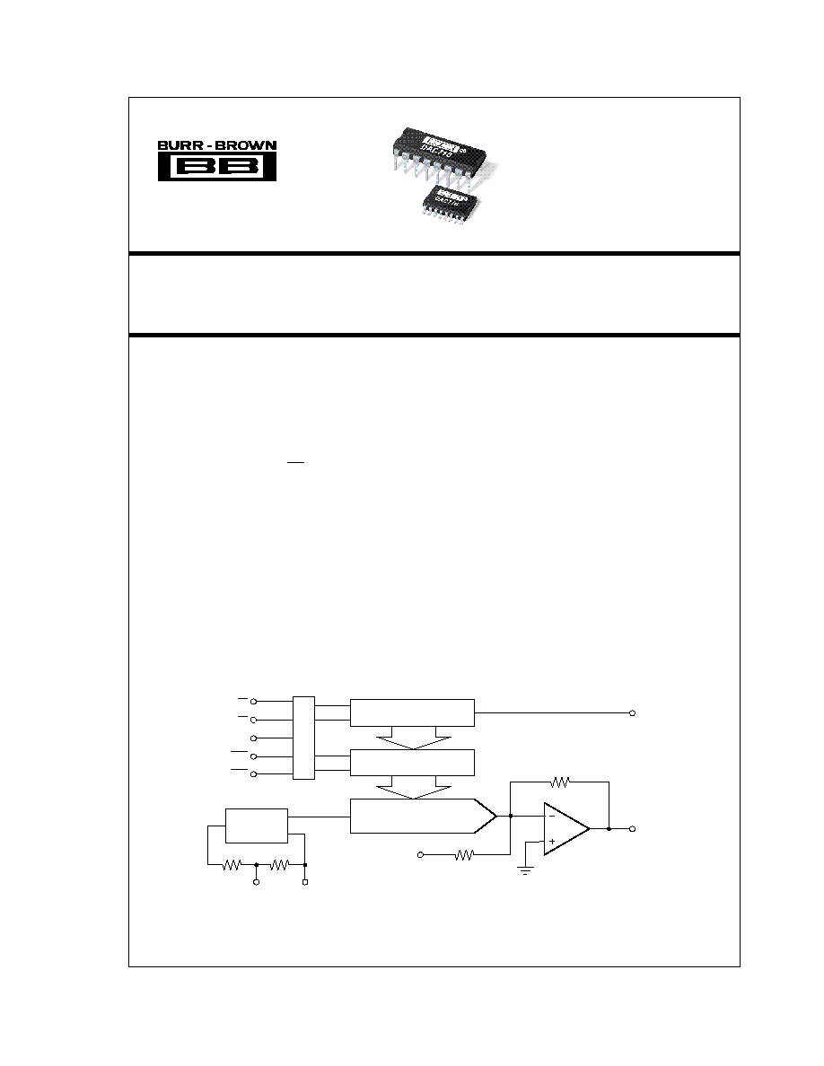
DAC716
16-Bit DIGITAL-TO-ANALOG CONVERTER
with Serial Data Interface
DESCRIPTION
The DAC716 is a complete monolithic D/A converter
including a +10V temperature compensated voltage
reference, current-to-voltage amplifier, a high-speed
synchronous serial interface, a serial output which
allows cascading multiple converters, and an asyn-
chronous clear function which immediately sets the
output voltage to zero.
The output voltage range is 0 to +10V while operating
from
±
12V to
±
15V supplies, and the gain and bipolar
offset adjustments are designed so that they can be set
via external potentiometers or external D/A convert-
ers. The output amplifier is protected against short-
circuiting to ground.
The 16-pin DAC716 is available in a plastic 0.3" DIP
and a wide-body plastic SOIC package. The DAC716P,
U, PB, and UB are specified over the ≠40
∞
C to +85
∞
C
range while the DAC716UK and PK are specified
over the 0
∞
C to +70
∞
C range.
Æ
© 1996 Burr-Brown Corporation
PDS-1324B
Printed in U.S.A. March, 1998
FEATURES:
q
SERIAL DIGITAL INTERFACE
q
VOLTAGE OUTPUT: 0 to +10V
q
±
2 LSB INTEGRAL LINEARITY
q
PRECISION INTERNAL REFERENCE
q
LOW NOISE: 120nV/
Hz Including Reference
q
16-LEAD PLASTIC SKINNY DIP AND PLASTIC
SOIC PACKAGES
V
OUT
V
REF OUT
+10V
Reference
Circuit
16-Bit D/A Converter
D/A Latch
SDO
16
Input Shift Register
16
A
1
SDI
CLK
CLR
A
0
Offset Adjust
Gain
Adjust
International Airport Industrial Park ∑ Mailing Address: PO Box 11400, Tucson, AZ 85734 ∑ Street Address: 6730 S. Tucson Blvd., Tucson, AZ 85706 ∑ Tel: (520) 746-1111 ∑ Twx: 910-952-1111
Internet: http://www.burr-brown.com/ ∑ FAXLine: (800) 548-6133 (US/Canada Only) ∑ Cable: BBRCORP ∑ Telex: 066-6491 ∑ FAX: (520) 889-1510 ∑ Immediate Product Info: (800) 548-6132

2
Æ
DAC716
SPECIFICATIONS
At T
A
= +25
∞
C, +V
CC
= +15V, ≠V
CC
= ≠15V, unless otherwise noted.
Straight Binary
DAC716P, U
DAC716PB, UB
DAC716PK, UK
PARAMETER
MIN
TYP
MAX
MIN
TYP
MAX
MIN
TYP
MAX
UNITS
TRANSFER CHARACTERISTICS
ACCURACY
Linearity Error
±
4
±
2
±
2
LSB
T
MIN
to T
MAX
±
8
±
4
±
2
LSB
Differential Linearity Error
±
4
±
2
±
2
LSB
T
MIN
to T
MAX
±
8
±
4
±
2
LSB
Monotonicity
14
15
15
Bits
Monotonicity Over Spec Temp Range
13
14
15
Bits
Gain Error
(3)
±
0.1
T
T
%
T
MIN
to T
MAX
±
0.25
T
T
%
Unipolar Zero Error
(3)
±
0.1
T
T
% of FSR
(2)
T
MIN
to T
MAX
±
0.2
T
T
% of FSR
Power Supply Sensitivity of Gain
±
0.003
T
T
%FSR/%V
CC
±
30
T
T
ppm FSR/%V
CC
DYNAMIC PERFORMANCE
Settling Time
(to
±
0.003%FSR, 5kW || 500pF Load)
(4)
20V Output Step
6
10
T
T
T
T
µ
s
1LSB Output Step
(5)
4
T
T
µ
s
Output Slew Rate
10
T
T
V/
µ
s
Total Harmonic Distortion
0dB, 1001Hz, f
S
= 100kHz
0.005
T
T
%
≠20dB, 1001Hz, f
S
= 100kHz
0.03
T
T
%
≠60dB, 1001Hz, f
S
= 100kHz
3.0
T
T
%
SINAD: 1001Hz, f
S
= 100kHz
87
T
T
dB
Digital Feedthrough
(5)
2
T
T
nV≠s
Digital-to-Analog Glitch Impulse
(5)
15
T
T
nV≠s
Output Noise Voltage (includes reference)
120
T
T
nV/
Hz
ANALOG OUTPUT
Output Voltage Range
+V
CC
, ≠V
CC
=
±
11.4V
+10
T
T
V
Output Current
±
5
T
T
mA
Output Impedance
0.1
T
T
W
Short Circuit to ACOM Duration
Indefinite
T
T
REFERENCE VOLTAGE
Voltage
+9.975
+10.000
+10.025
T
T
T
T
T
T
V
T
MIN
to T
MAX
+9.960
+10.040
T
T
T
T
V
Output Resistance
1
T
T
W
Source Current
2
T
T
mA
Short Circuit to ACOM Duration
Indefinite
T
T
INTERFACE
RESOLUTION
16
T
T
Bits
DIGITAL INPUTS
Serial Data Input Code
Logic Levels
(1)
V
IH
+2.0
(V
CC
≠1.4)
T
T
T
T
V
V
IL
0
+0.8
T
T
T
T
V
I
IH
(V
I
= +2.7V)
±
10
T
T
µ
A
I
IL
(V
I
= +0.4V)
±
10
T
T
µ
A
DIGITAL OUTPUT
Serial Data
V
OL
(I
SINK
= 1.6mA)
0
+0.4
T
T
T
T
V
V
OH
(I
SOURCE
= 500
µ
A),T
MIN
to T
MAX
+2.4
+5
T
T
T
T
V
POWER SUPPLY REQUIREMENTS
Voltage
+V
CC
+11.4
+15
+16.5
T
T
T
T
T
T
V
≠V
CC
≠11.4
≠15
≠16.5
T
T
T
T
T
T
V
Current (No Load,
±
15V Supplies)
(6)
+V
CC
13
16
T
T
T
T
mA
≠V
CC
22
26
T
T
T
T
mA
Power Dissipation
(7)
625
T
T
mW
TEMPERATURE RANGES
Specification
All Grades
≠40
+85
T
T
0
+70
∞
C
Storage
≠60
+150
T
T
T
T
∞
C
Thermal Coefficient,
JA
75
T
T
∞
C/W
T
Specifications are the same as the grade to the left.
NOTES: (1) Digital inputs are TTL and +5V CMOS compatible over the specification temperature range. (2) FSR means Full Scale Range. For example, for 0 to +10V output, FSR = 10V. (3) Errors externally
adjustable to zero. (4) Maximum represents the 3
limit. Not 100% tested for this parameter. (5) For the worst-case Straight Binary code changes: 7FFF to 8000 and 8000 to 7FFF. (6) During power supply
turn on, the transient supply current may approach 3x the maximum quiescent specification. (7) Typical (i.e. rated) supply voltages times maximum currents.

3
Æ
DAC716
DIFFERENTIAL
LINEARITY ERROR
TEMPERATURE
PRODUCT
PACKAGE
T
MIN
to T
MAX
RANGE
DAC716P
Plastic DIP
±
8 LSB
≠40
∞
C to +85
∞
C
DAC716U
Plastic SOIC
±
8 LSB
≠40
∞
C to +85
∞
C
DAC716PB
Plastic DIP
±
4 LSB
≠40
∞
C to +85
∞
C
DAC716UB
Plastic SOIC
±
4 LSB
≠40
∞
C to +85
∞
C
DAC716PK
Plastic DIP
±
2 LSB
0
∞
C to +70
∞
C
DAC716UK
Plastic SOIC
±
2 LSB
0
∞
C to +70
∞
C
PIN CONFIGURATION
Top View
ELECTROSTATIC
DISCHARGE SENSITIVITY
Electrostatic discharge can cause damage ranging from per-
formance degradation to complete device failure. Burr-
Brown Corporation recommends that all integrated circuits
be handled and stored using appropriate ESD protection
methods.
ESD damage can range from subtle performance degrada-
tion to complete device failure. Precision integrated circuits
may be more susceptible to damage because very small
parametric changes could cause the device not to meet
published specifications.
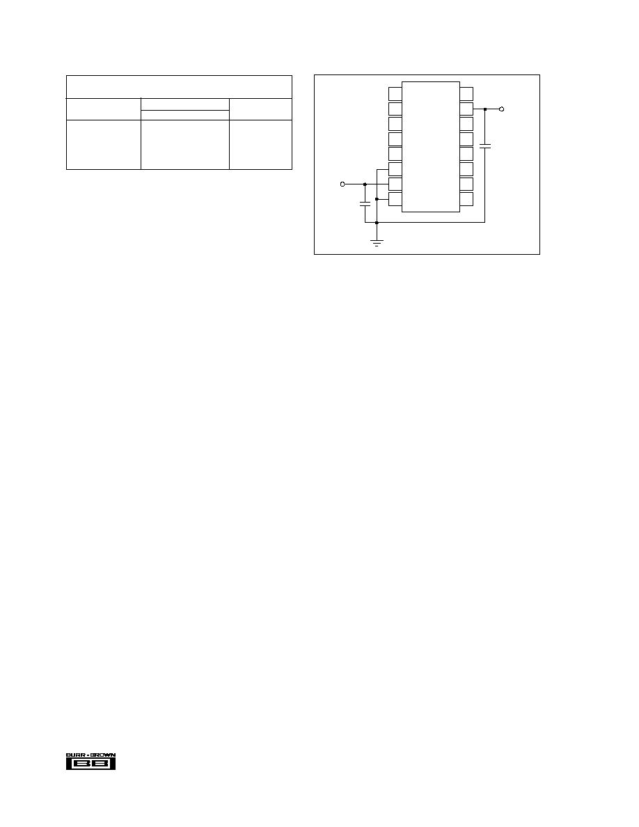
PIN DESCRIPTIONS
PIN
LABEL
DESCRIPTION
1
CLK
Serial Data Clock
2
A
0
Enable for Input Register (Active Low)
3
A
1
Enable for D/A Latch (Active Low)
4
SDI
Serial Data Input
5
SDO
Serial Data Output
6
DCOM
Digital Supply Ground
7
+V
CC
Positive Power Supply
8
ACOM
Analog Supply Ground
9
V
OUT
D/A Output
10
NC
No Connection
11
NC
No Connection
12
V
REF OUT
Voltage Reference Output
13
Offset Adjust
Offset Adjust
14
Gain Adjust
Gain Adjust
15
≠V
CC
Negative Power Supply
16
CLR
Clear
ORDERING INFORMATION
SOIC/DIP
+V
CC
to Common .................................................................... 0V to +17V
≠V
CC
to Common .................................................................... 0V to ≠17V
+V
CC
to ≠V
CC
....................................................................................... 34V
ACOM to DCOM ...............................................................................
±
0.5V
Digital Inputs to Common ............................................. ≠1V to (V
CC
≠0.7V)
External Voltage Applied to BPO and Range Resistors .....................
±
V
CC
V
REF OUT
......................................................... Indefinite Short to Common
V
OUT
............................................................... Indefinite Short to Common
SDO ............................................................... Indefinite Short to Common
Power Dissipation .......................................................................... 750mW
Storage Temperature ...................................................... ≠60
∞
C to +150
∞
C
Lead Temperature (soldering, 10s) ................................................ +300
∞
C
NOTE: (1) Stresses above those listed under "Absolute Maximum Ratings"
may cause permanent damage to the device. Exposure to absolute maximum
conditions for extended periods may affect device reliability.
ABSOLUTE MAXIMUM RATINGS
(1)
CLK
A
0
A
1
SDI
SDO
DCOM
+V
CC
ACOM
DAC716
CLR
≠V
CC
Gain Adjust
Offset Adjust
V
REF OUT
NC
NC
V
OUT
1
2
3
4
5
6
7
8
16
15
14
13
12
11
10
9
The information provided herein is believed to be reliable; however, BURR-BROWN assumes no responsibility for inaccuracies or omissions. BURR-BROWN assumes
no responsibility for the use of this information, and all use of such information shall be entirely at the user's own risk. Prices and specifications are subject to change
without notice. No patent rights or licenses to any of the circuits described herein are implied or granted to any third party. BURR-BROWN does not authorize or warrant
any BURR-BROWN product for use in life support devices and/or systems.
PACKAGE DRAWING
PRODUCT
PACKAGE
NUMBER
(1)
DAC716P
Plastic DIP
180
DAC716U
Plastic SOIC
211
NOTE: (1) For detailed drawing and dimension table, please see end of data sheet,
or Appendix C of Burr-Brown IC Data Book.
PACKAGE INFORMATION
4
Æ
DAC716
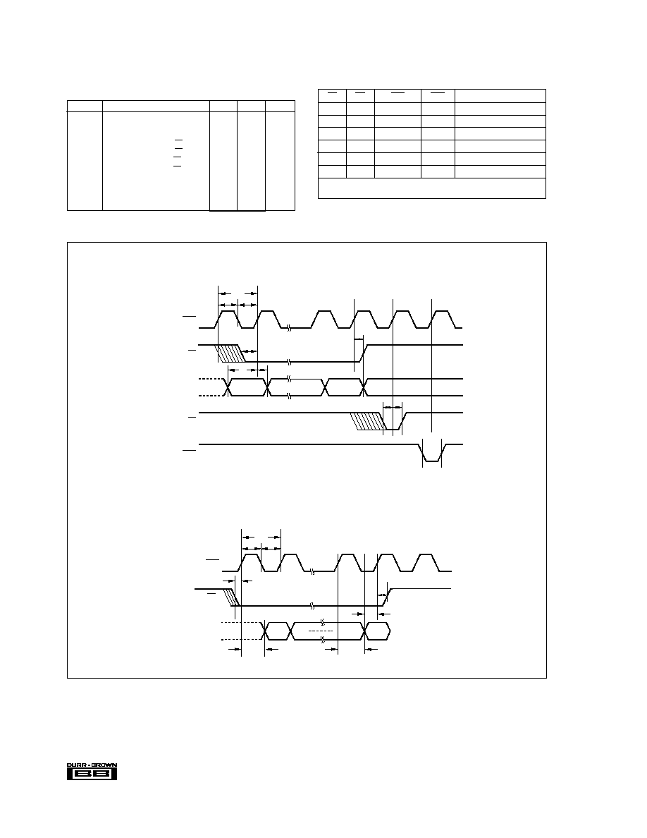
TIMING SPECIFICATIONS
T
A
= ≠40
∞
C to +85
∞
C, +V
CC
= +15V, ≠V
CC
= ≠15V.
SYMBOL
PARAMETER
MIN
MAX
UNITS
t
CLK
Data Clock Period
100
ns
t
CL
Clock LOW
50
ns
t
CH
Clock HIGH
50
ns
t
A0S
Setup Time for A
0
50
ns
t
A1S
Setup Time for A
1
50
ns
t
AOH
Hold Time for A
0
10
ns
t
A1H
Hold Time for A
1
10
ns
t
DS
Setup Time for DATA
50
ns
t
DH
Hold Time for DATA
10
ns
t
DSOP
Output Propagation Delay
140
ns
t
CP
Clear Pulsewidth
200
ns
A
0
A
1
CLK
CLR
DESCRIPTION
0
1
1
0
1
1
Shift Serial Data into SDI
1
0
1
0
1
1
Load D/A Latch
1
1
1
0
1
1
No Change
0
0
1
0
1
1
Two Wire Operation
(1)
X
X
1
1
No Change
X
X
X
0
Reset D/A Latch
NOTES: X = Don't Care. (1) All digital input changes will appear at the
D/A output.
TRUTH TABLE
TIMING DIAGRAMS
Serial Data In
Serial Data Out
CLK
A
0
SDO
Serial Data Out
t
A0H
t
A0S
D
0
D
14
D
15
t
CLK
t
CH
t
CL
t
DS
t
DSOP
t
DSOP
CLK
A
0
SDI
Serial Data Input
MSB First
Latch Data
In D/A Latch
A
1
t
A0H
D
0
D
14
D
15
t
A1S
t
A1H
t
DH
t
DS
t
A0S
t
CLK
t
CP
t
CH
t
CL
CLR
5
Æ
DAC716
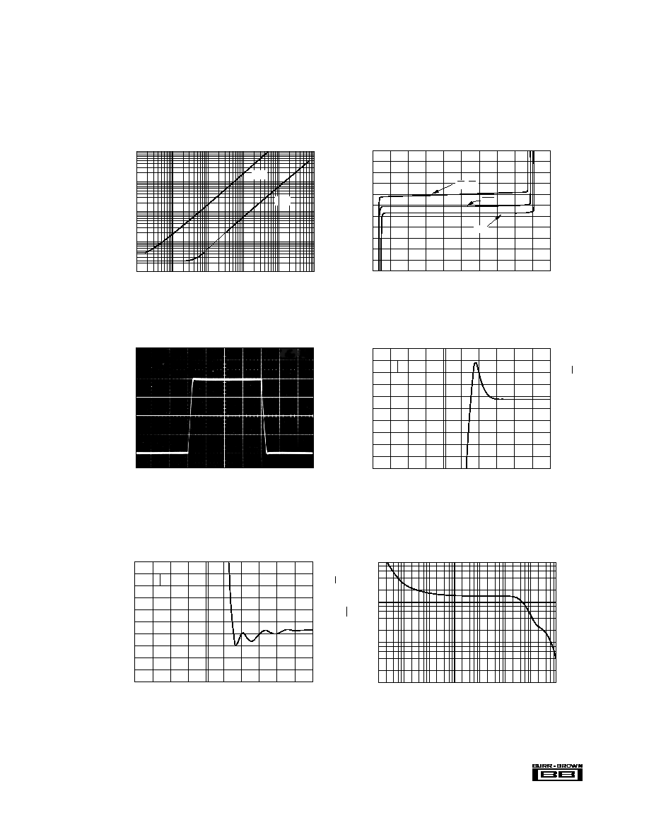
Frequency (Hz)
[Change in FSR]/[Change in Supply Voltage]
1k
10
100
1k
10k
100k
1M
POWER SUPPLY REJECTION vs
POWER SUPPLY RIPPLE FREQUENCY
(ppm of FSR/ %)
100
10
1
0.1
+V
CC
≠V
CC
TYPICAL PERFORMANCE CURVES
At T
A
= +25
∞
C, V
CC
=
±
15V, unless otherwise noted.
1000
100
10
1
1
10
100
1k
10k
100k
1M
10M
Frequency (Hz)
nV/
Hz
V
OUT
SPECTRAL NOISE DENSITY
10
0
Time (10µs/div)
FULL SCALE OUTPUT SWING
V (V)
OUT
A
1
SETTLING TIME, +10V TO 0V
Time (1µs/div)
2500
2000
1500
1000
500
0
≠500
≠1000
≠1500
≠2000
≠2500
Around 0 (µV)
+5V
0V
A
1
SETTLING TIME, 0V TO +10V
Time (1µs/div)
2500
2000
1500
1000
500
0
≠500
≠1000
≠1500
≠2000
≠2500
Around +10V (µV)
+5V
≠0V
2.0
≠0.85
0
2.55
4.25
5.95
6.8
LOGIC vs V LEVEL
1.0
0
≠1.0
≠2.0
0.85
1.7
3.4
5.1
SDI
A
0
, A
1
CLR
V Digital Input
I Digital Input (µA)
FPO

6
Æ
DAC716
DISCUSSION OF
SPECIFICATIONS
LINEARITY ERROR
Linearity error is defined as the deviation of the analog
output from a straight line drawn between the end points of
the transfer characteristic.
DIFFERENTIAL LINEARITY ERROR
Differential linearity error (DLE) is the deviation from
1LSB of an output change from one adjacent state to the
next. A DLE specification of
±
1/2LSB means that the output
step size can range from 1/2LSB to 3/2LSB when the digital
input code changes from one code word to the adjacent code
word. If the DLE is more positive than ≠1LSB, the D/A is
said to be monotonic.
MONOTONICITY
A D/A converter is monotonic if the output either increases
or remains the same for increasing digital input values.
Monotonicity of the K grade is guaranteed over the specifi-
cation temperature range to 15 bits.
SETTLING TIME
Settling time is the total time (including slew time) for the
D/A output to settle to within an error band around its final
value after a change in input. Settling times are specified to
within
±
0.003% of Full Scale Range (FSR) for an output
step change of 10V and 1LSB. The 1LSB change is mea-
sured at the Major Carry (7FFF to 8000, and 8000 to 7FFF:
Straight Binary codes), the input transition at which worst-
case settling time occurs.
TOTAL HARMONIC DISTORTION + NOISE
Total harmonic distortion + noise is defined as the ratio of
the square root of the sum of the squares of the values of the
harmonics and noise to the value of the fundamental fre-
quency. It is expressed in % of the fundamental frequency
amplitude at sampling rate f
S
.
SIGNAL-TO-NOISE
AND DISTORTION RATIO (SINAD)
SINAD includes all the harmonic and outstanding spurious
components in the definition of output noise power in
addition to quantizing and internal random noise power.
SINAD is expressed in dB at a specified input frequency and
sampling rate, f
S
.
DIGITAL-TO-ANALOG GLITCH IMPULSE
The amount of charge injected into the analog output from
the digital inputs when the inputs change state. It is mea-
sured at half scale at the input codes where as many as
possible switches change state--from 8000 to 7FFF.
DIGITAL FEEDTHROUGH
When the A/D is not selected, high frequency logic activity
on the digital inputs is coupled through the device and shows
up as output noise. This noise is digital feedthrough.
OPERATION
The DAC716 is a monolithic integrated-circuit 16-bit D/A
converter complete with 16-bit D/A switches and ladder
network, voltage reference, output amplifier and a serial
interface.
INTERFACE LOGIC
The DAC716 has double-buffered data latches. The input
data latch holds a 16-bit data word before loading it into the
second latch, the D/A latch. This double-buffered organiza-
tion permits simultaneous update of several D/A converters.
All digital control inputs are active low. Refer to block
diagram of Figure 1.
All latches are level-triggered. Data present when the enable
inputs are logic "0" will enter the latch. When the enable
inputs return to logic "1", the data is latched.
The CLR input resets both the input latch and the D/A latch
to give an output voltage of 0V (code 0000).
LOGIC INPUT COMPATIBILITY
DAC716 digital inputs are TTL compatible (1.4V switching
level) with low leakage, high impedance inputs. Thus the
inputs are suitable for being driven by any type of 5V logic
such as 5V CMOS logic. An equivalent circuit of a digital
input is shown in Figure 2.
Data inputs will float to logic "0" and control inputs will
float to logic "0" if left unconnected. It is recommended that
any unused inputs be connected to DCOM to improve noise
immunity.
Digital inputs remain high impedance when power is off.
INPUT CODING
The DAC716 is designed to accept Straight Binary (SB)
input codes. The serial input format is MSB first.
INTERNAL REFERENCE
DAC716 contains a +10V reference.
The reference output may be used to drive external loads,
sourcing up to 2mA. The load current should be constant,
otherwise the gain and unipolar offset of the converter will
vary.
OUTPUT VOLTAGE SWING
The output amplifier of DAC716 is designed to achieve a
+10V output range. DAC716 will provide a +10V output
swing while operating on
±
11.4V or higher voltage supplies.
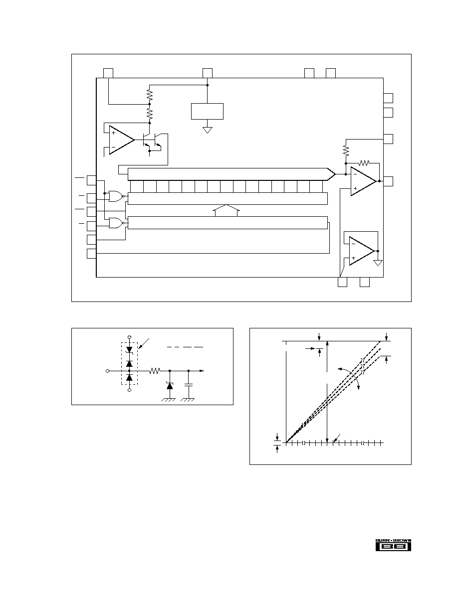
7
Æ
DAC716
FIGURE 1. DAC716 Block Diagram.
FIGURE 2. Equivalent Circuit of Digital Inputs.
FIGURE 3. Relationship of Offset and Gain Adjustments.
Gain Adjustment
Apply the digital input that gives the maximum positive
voltage output. Adjust the gain potentiometer or the gain
adjust D/A converter for this positive full scale voltage.
GAIN AND OFFSET ADJUSTMENTS
Figure 3 illustrates the relationship of offset and gain adjust-
ments for a unipolar connected D/A converter. Offset should
be adjusted first to avoid interaction of adjustments. See
Table I for calibration values and codes. These adjustments
have a minimum range of
±
0.3%.
Offset Adjustment
Apply the digital input code, 0000, that produces 0V and adjust
the offset potentiometer or the offset adjust D/A converter for
0V.
Shift Register
DAC Latch
14
12
+10V
Reference
8
6
7
DCOM
+V
CC
ACOM
V
REF OUT
Gain Adjust
4
SDI
5
SDO
16
2
A
0
3
A
1
1
16
CLK
CLR
15
≠ V
CC
Offset
Adjust
13
NC
11
NC
10
9
V
OUT
D/A Switches
≠V
CC
+2.5V
15k
180
9.75k
5k
R
R = 1k
: A
0
, A
1
, CLK, CLR, SDI
ESD Protection Circuit
6.8V
5pF
Digital
Input
≠V
CC
+V
CC
1LSB
Range of
Offset Adjust
Offset Adj.
Translates
the Line
Digital Input
FFFF
H
8000
H
0000
H
Analog Output
Full Scale
Range
Gain Adjust
Rotates the Line
Zero
Range of
Gain Adjust
±0.3%
±0.3%
+ Full Scale
8
Æ
DAC716
DAC716 CALIBRATION VALUES
1 LEAST SIGNIFICANT BIT = 152
µ
V
DIGITAL INPUT CODE
ANALOG OUTPUT (V)
STRAIGHT BINARY
UNIPOLAR 10V RANGE
DESCRIPTION
FFFF
H
+9.999695
+ Full Scale ≠1LSB
|
8000
H
+5.000000
Half Scale
0000
H
0.000000
Unipolar Zero
TABLE I. Digital Input and Analog Output Voltage Calibra-
tion Values.
INSTALLATION
GENERAL CONSIDERATIONS
Due to the high precision of these D/A converters, system
design problems such as grounding and contact resistance
become very important. A 16-bit converter with a 10V full-
scale range has a 1LSB value of 152
µ
V. With a load current
of 5mA, series wiring and connector resistance of only
60m
will cause a voltage drop of 300
µ
V. To understand
what this means in terms of a system layout, the resistivity
of a typical 1 ounce copper-clad printed circuit board is 1/2
m
per square. For a 5mA load, a 0.1 inch wide printed
circuit conductor 0.6 inches long will result in a voltage drop
of 150
µ
V.
The analog output of DAC716 has an LSB size of 152
µ
V
(≠96dB). The rms noise floor of the D/A should remain below
this level in the frequency range of interest. The DAC716's
output noise spectral density (which includes the noise contrib-
uted by the internal reference) is shown in the Typical Perfor-
mance Curves section.
Wiring to high-resolution D/A converters should be routed
to provide optimum isolation from sources of RFI and EMI.
The key to elimination of RF radiation or pickup is small
loop area. Signal leads and their return conductors should be
kept close together such that they present a small capture
cross-section for any external field. Wire-wrap construction
is not recommended.
POWER SUPPLY AND
REFERENCE CONNECTIONS
Power supply decoupling capacitors should be added as
shown in Figure 4. Best performance occurs using a 1 to
10
µ
F tantalum capacitor at ≠V
CC
. Applications with less
critical settling time may be able to use 0.01
µ
F at ≠V
CC
as well as at +V
CC
. The capacitors should be located
close to the package.
The DAC716 has separate ANALOG COMMON and DIGI-
TAL COMMON pins. The current through DCOM is mostly
switching transients and are up to 1mA peak in amplitude.
The current through ACOM is typically 5
µ
A for all codes.
Use separate analog and digital ground planes with a single
interconnection point to minimize ground loops. The analog
FIGURE 4. Power Supply Connections.
1
2
3
4
5
6
7
8
16
15
14
13
12
11
10
9
1µF
1µF
DAC716
DCOM
+V
CC
ACOM
≠V
CC
+12V to +15V
≠12V to ≠15V
+
+
pins are located adjacent to each other to help isolate analog
from digital signals. Analog signals should be routed as far
as possible from digital signals and should cross them at
right angles. A solid analog ground plane around the D/A
package, as well as under it in the vicinity of the analog and
power supply pins, will isolate the D/A from switching
currents. It is recommended that DCOM and ACOM be
connected directly to the ground planes under the package.
If several DAC716s are used or if the DAC716 shares
supplies with other components, connecting the ACOM and
DCOM lines together at the power supplies only rather than
at each chip, may give better results.
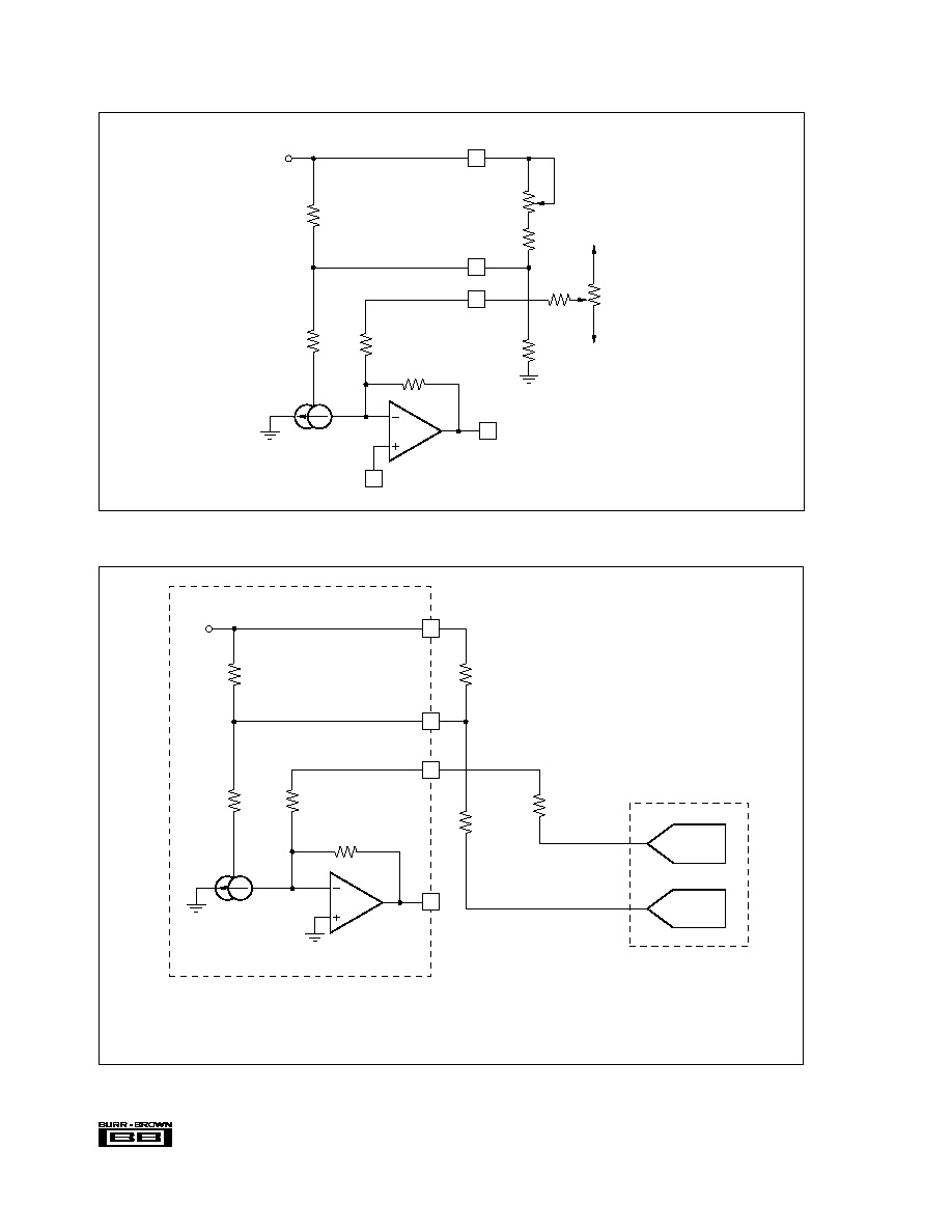
LOAD CONNECTIONS
Since the reference point for V
OUT
and V
REF
OUT
is the
ACOM pin, it is important to connect the D/A converter load
directly to the ACOM pin. Refer to Figure 5.
Lead and contact resistances are represented by R
1
through
R
3
. As long as the load resistance R
L
is constant, R
1
simply
introduces a gain error and can be removed by gain adjust-
ment of the D/A or system-wide gain calibration. R
2
is part
of R
L
if the output voltage is sensed at ACOM.
In some applications it is impractical to return the load to the
ACOM pin of the D/A converter. Sensing the output voltage
at the SYSTEM GROUND point is reasonable, because there
is no change in DAC716 ACOM current, provided that R
3
is
a low-resistance ground plane or conductor. In this case you
may wish to connect DCOM to SYSTEM GROUND as well.
GAIN AND OFFSET ADJUST
Connections Using Potentiometers
GAIN and OFFSET adjust pins provide for trim using
external potentiometers. 15-turn potentiometers provide suf-
ficient resolution. Range of adjustment of these trims is at
least
±
0.3% of Full Scale Range. Refer to Figure 6.

9
Æ
DAC716
Using D/A Converters
The GAIN ADJUST and OFFSET ADJUST circuits of
DAC716 have been arranged so that these points may be
easily driven by external D/A converters. Refer to
Figure 7. 12-bit D/A converters provide a nominal
OFFSET adjust and GAIN adjust resolution of 25
µ
V and
15
µ
V per LSB step, respectively.
Nominal values of GAIN and OFFSET occur when the D/A
converters outputs are at approximately half scale, 0V.
OUTPUT VOLTAGE RANGE CONNECTIONS
The DAC716 output amplifier is connected internally for
10V output range.
DIGITAL INTERFACE
SERIAL INTERFACE
The DAC716 has a serial interface with two data buffers
which can be used for either synchronous or asynchronous
updating of multiple D/A converters. A0 is the enable control
for the Data Input Latch. A1 is the enable for the D/A Latch.
CLK is used to strobe data into the latches enabled by A0 and
A1. A CLR function is also provided and when enabled it sets
both the Data Latch and the D/A Latch to all zeros .
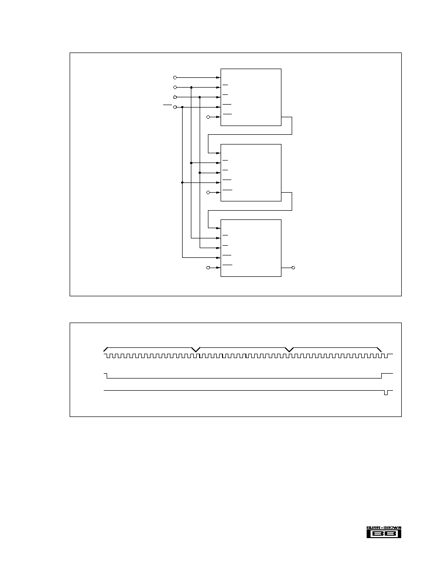
Multiple DAC716s can be connected to the same CLK and
data lines in two ways. The output of the serial loaded data
latch is available as SDO so that any number of DAC716s
can be cascaded on the same input bit stream as shown in
Figure 8 and 9. This configuration allows all D/A converters
to be updated simultaneously and requires a minimum num-
ber of control signal inputs. These configurations do require
16N CLK cycles to load any given D/A converter, where N
is the number of D/A converters.
The DAC716 can also be connected in parallel as shown in
Figure 10. This configuration allows any D/A converter in
the system to be updated in a maximum of 16 CLK cycles.
FIGURE 5. System Ground Considerations for High-Resolution D/A Converters.
R
1
Sense
Output
R
L
R
2
R
3
Alternate Ground
Sense Connection
System Ground
ACOM
DCOM
Bus
Interface
DAC716
Analog
Power
Supply
0.01µF
(1)
0.01µF
To +V
CC
To ≠V
CC
NOTE: (1) Locate close to DAC716 package.
V
OUT
5k
9.75k
V
REF
V
REF OUT
Offset Adjust
SDI
A
0
A
1
CLR
10
Æ
DAC716
FIGURE 6. Manual Offset and Gain Adjust Circuits.
For no external adjustments, pins 13 and 14 are not connected.
External resistors R
1
- R
3
are standard
±
1% values. Range of
adjustment at least
±
0.3% FSR.
FIGURE 7. Gain and Offset Adjustment Using D/A Converters.
For no external adjustments, pins 13 and 14 are not connected.
External resistors R
1
- R
3
tolerance:
±
1%. Range of adjustment at
least
±
0.3% FSR.
5k
9
13
14
10V V
OUT
9.75k
IDAC
0-2mA
15k
R
3
27k
R
2
1M
+V
CC
≠V
CC
P
1
1k
R
1
100
12
180
P
2
10k
to 100k
Internal
+10V Reference
V
REF OUT
Gain Adjust
Offset Adjust
8
ACOM
5k
9
13
14
+10V V
OUT
DAC716
9.75k
IDAC
0-2mA
15k
R
2
33k
≠10 to +10V
R
3
1M
180
Internal
+10V Reference
V
REF OUT
Gain Adjust
Offset Adjust
R
1
392
12
DAC
±10V
DAC
±10V
≠10 to +10V
11
Æ
DAC716
FIGURE 8a. Cascaded Serial Bus Connection with Synchronous Update.
FIGURE 8b. Timing Diagram For Figure 8a.
F E D C B A 9
8
7
6 5 4
3
2
1 0 F E D C B A 9
8
7
6
5 4 3
2 1
0 F E D C B A 9 8
7
6 5
4
3 2 1
0
Clock
Data
Data Latch
Update
DAC 3
DAC 2
DAC 1
SDI
A0
A1
CLK
CLR
DAC716
DAC 1
SDO
Data
Data Latch
Up Date
CLK
4
2
3
1
16
+5V
SDI
A0
A1
CLK
CLR
DAC716
DAC 2
SDO
4
2
3
1
16
+5V
SDI
A0
A1
CLK
CLR
DAC716
DAC 3
SDO
4
2
3
1
16
+5V
5
5
5
To other DACs

12
Æ
DAC716
FIGURE 9a. Cascaded Serial Bus Connection with Asynchronous Update.
FIGURE 9b. Timing Diagram For Figure 9a.
F E D C B A 9
8
7
6 5 4
3
2
1 0 F E D C B A 9
8
7
6
5 4 3
2 1
0 F E D C B A 9 8
7
6 5
4
3 2 1
0
Update
DAC 3
DAC 2
DAC 1
Data Latch
Data
SDI
A0
A1
CLK
CLR
DAC716
DAC 1
DAC716
DAC 2
DAC716
DAC 3
SDO
Data
Data Latch
Up Date
4
2
3
1
16
+5V
SDI
A0
A1
CLK
CLR
SDO
4
2
3
1
16
+5V
SDI
A0
A1
CLK
CLR
SDO
4
2
3
1
16
+5V
5
5
5
To other DACs

13
Æ
DAC716
FIGURE 10a. Parallel Bus Connection.
FIGURE 10b. Timing Diagram For Figure 10a.
F E D C B A 9
8
7
6 5 4
3
2
1 0 F E D C B A 9
8
7
6
5 4 3
2 1
0 F E D C B A 9 8
7
6 5
4
3 2 1
0
Clock
Data
Data Latch 1
Data Latch 2
Data Latch 3
Update
DAC 1
DAC 2
DAC 3
SDI
A0
A1
CLK
CLR
DAC716
DAC 1
DAC716
DAC 2
DAC716
DAC 3
SDO
Data
Data Latch 1
Data Latch 2
Data Latch 3
Up Date
CLK
4
2
3
1
16
SDI
A0
A1
CLK
CLR
SDO
4
2
3
1
16
SDI
A0
A1
CLK
CLR
SDO
4
2
3
1
16
5
5
5
CLR