 | ÐлекÑÑоннÑй компоненÑ: DAC7545 | СкаÑаÑÑ:  PDF PDF  ZIP ZIP |
Äîêóìåíòàöèÿ è îïèñàíèÿ www.docs.chipfind.ru
1
DAC7545
CMOS 12-Bit Multiplying
DIGITAL-TO-ANALOG CONVERTER
Microprocessor Compatible
FEATURES
q
FOUR-QUADRANT MULTIPLICATION
q
LOW GAIN TC: 2ppm/
°
C typ
q
MONOTONICITY GUARANTEED OVER
TEMPERATURE
q
SINGLE 5V TO 15V SUPPLY
q
TTL/CMOS LOGIC COMPATIBLE
q
LOW OUTPUT LEAKAGE: 10nA max
q
LOW OUTPUT CAPACITANCE: 70pF max
q
DIRECT REPLACEMENT FOR AD7545,
PM-7545
DESCRIPTION
The DAC7545 is a low-cost CMOS, 12-bit four-
quadrant multiplying, digital-to-analog converter with
input data latches. The input data is loaded into the
DAC as a 12-bit data word. The data flows through to
the DAC when both the chip select (CS) and the write
(WR) pins are at a logic low.
Laser-trimmed thin-film resistors and excellent CMOS
voltage switches provide true 12-bit integral and dif-
ferential linearity. The device operates on a single
+5V to +15V supply and is available in 20-pin plastic
DIP or 20-lead plastic SOIC packages. Devices are
specified over the commercial.
The DAC7545 is well suited for battery or other low
power applications because the power dissipation is
less than 0.5mW when used with CMOS logic inputs
and V
DD
= +5V.
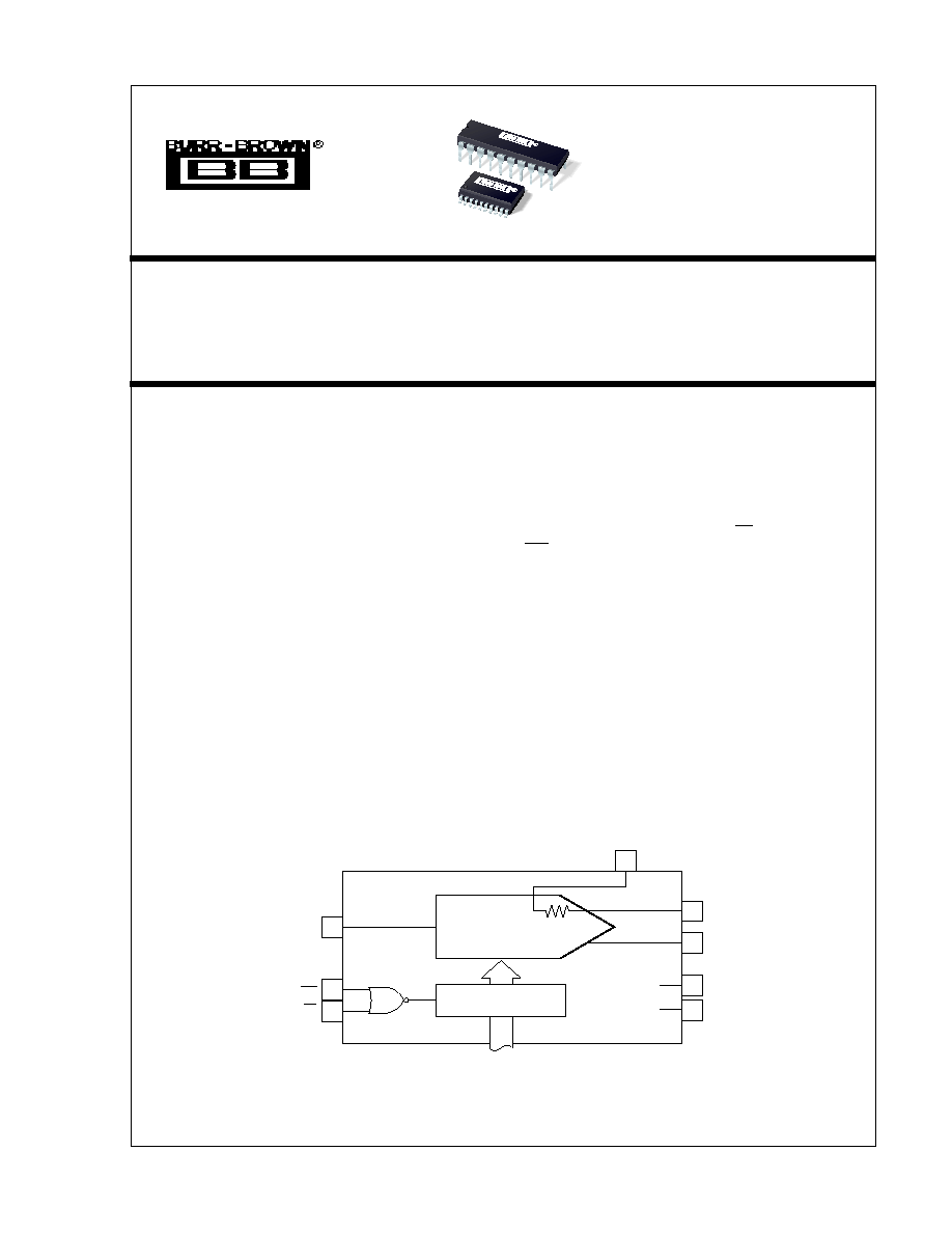
12-Bit
Multiplying DAC
AGND
OUT 1
DB
11
-DB
0
(Pins 4-15)
WR
CS
17
Input
Data Latches
12
12
16
19
V
REF
20
R
FB
1
2
18
3
V
DD
DGND
DAC7545
International Airport Industrial Park · Mailing Address: PO Box 11400, Tucson, AZ 85734 · Street Address: 6730 S. Tucson Blvd., Tucson, AZ 85706 · Tel: (520) 746-1111 · Twx: 910-952-1111
Internet: http://www.burr-brown.com/ · FAXLine: (800) 548-6133 (US/Canada Only) · Cable: BBRCORP · Telex: 066-6491 · FAX: (520) 889-1510 · Immediate Product Info: (800) 548-6132
©
1987 Burr-Brown Corporation
PDS-747F
Printed in U.S.A. August, 1997
DAC7545
DAC7545
2
DAC7545
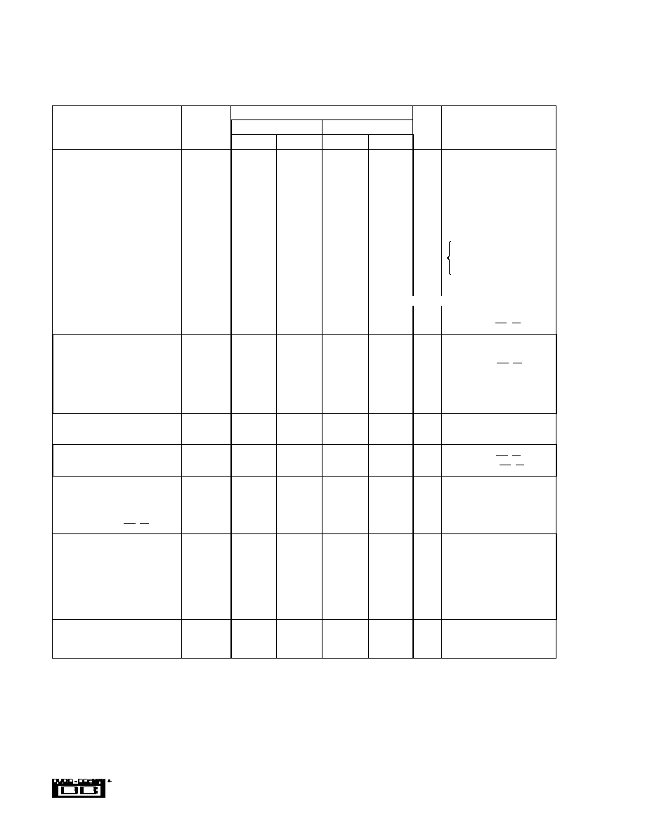
SPECIFICATIONS
ELECTRICAL
V
REF
= +10V, V
OUT 1
= 0V, ACOM = DCOM, unless otherwise specified.
The information provided herein is believed to be reliable; however, BURR-BROWN assumes no responsibility for inaccuracies or omissions. BURR-BROWN
assumes no responsibility for the use of this information, and all use of such information shall be entirely at the user's own risk. Prices and specifications are subject
to change without notice. No patent rights or licenses to any of the circuits described herein are implied or granted to any third party. BURR-BROWN does not
authorize or warrant any BURR-BROWN product for use in life support devices and/or systems.
NOTES: (1) Temperature ranges--J, K, L, GL: 40
°
C to +85
°
C. (2) This includes the effect of 5ppm max, gain TC. (3) Guaranteed but not tested. (4) DB
0
-DB
11
= 0V
to V
DD
or V
DD
to 0V. (5) Typical. (6) Minimum. (7) Logic inputs are MOS gates. Typical input current (+25
°
C) is less than 1nA. (8) Sample tested at +25
°
C to ensure
compliance.
DAC7545
V
DD
= +5V
V
DD
= +15V
PARAMETER
GRADE
T
A
= +25
°
C
T
MAX
-T
MIN
(1)
T
A
= +25
°
C
T
MAX
-T
MIN
(1)
UNITS TEST CONDITIONS/COMMENTS
STATIC PERFORMANCE
Resolution
All
12
12
12
12
Bits
Accuracy
J
±
2
±
2
±
2
±
2
LSB
K
±
1
±
1
±
1
±
1
LSB
L
±
1/2
±
1/2
±
1/2
±
1/2
LSB
GL
±
1/2
±
1/2
±
1/2
±
1/2
LSB
Differential Nonlinearity
J
±
4
±
4
±
4
±
4
LSB
10-Bit Monotonic, T
MIN
to T
MAX
K
±
1
±
1
±
1
±
1
LSB
10-Bit Monotonic, T
MIN
to T
MAX
L
±
1
±
1
±
1
±
1
LSB
12-Bit Monotonic, T
MIN
to T
MAX
GL
±
1
±
1
±
1
±
1
LSB
12-Bit Monotonic, T
MIN
to T
MAX
Gain Error (with internal R
FB
)
(2)
J
±
20
±
20
±
25
±
25
LSB
D/A register loaded with FFF
H
.
K
±
10
±
10
±
15
±
15
LSB
Gain error is adjustable using
L
±
5
±
6
±
10
±
10
LSB
the circuits in Figures 2 and 3.
GL
±
2
±
3
±
6
±
7
LSB
Gain Temperature Coefficient
(3)
(
Gain/
Temperature)
All
±
5
±
5
±
10
±
10
ppm/
°
C Typical value is 2ppm/
°
C
for V
DD
= +5
DC Supply Rejection
(3)
(
Gain/
V
DD
)
All
0.015
0.03
0.01
0.02
%/%
V
DD
±
5%
Output Leakage Current at Out 1
J, K, L, GL
10
50
10
50
nA
DB
0
-DB
11
= 0V; WR, CS = 0V
DYNAMIC PERFORMANCE
Current Settling Time
(3)
All
2
2
2
2
µ
s
To 1/2LSB. Out
1
Load = 100
DAC output measured from
falling edge of WR. CS = 0V
Propagation Delay
(3)
(from digital input
All
change to 90% of final analog output)
300
250
ns
Out
1
Load = 100
. C
EXT
= 13pF
(4)
Glitch Energy
All
400
250
nV-s
(5)
V
REF
= ACOM
AC Feedback at I
OUT
1
All
5
5
5
5
mVp-p
(5)
V
REF
=
±
10V, 10kHz Sine Wave
REFERENCE INPUT
Input Resistance (pin 19 to AGND)
All
7
7
7
7
k
(6)
Input resistance TC = 300ppm/
°
C
(5)
25
25
25
25
k
AC OUTPUTS
Output Capacitance
(3)
: C
OUT 1
All
70
70
70
70
pF
DB
0
-DB
11
= 0V; WR, CS = 0V
C
OUT 2
All
200
200
200
200
pF
DB
0
-DB
11
= V
DD
; WR, CS = 0V
DIGITAL INPUTS
V
IH
(Input HIGH Voltage)
All
2.4
2.4
13.5
13.5
V
(6)
V
IL
(Input LOW Voltage)
All
0.8
0.8
1.5
1.5
V
I
IN
(Input Current)
(7)
All
±
1
±
10
±
1
±
10
µ
A
V
IN
= 0 or V
DD
Input Capacitance
(3)
: DB
0
-DB
11
All
5
5
5
5
pF
V
IN
= 0V
WR, CS
All
20
20
20
20
pF
V
IN
= 0V
SWITCHING CHARACTERISTICS
(8)
Chip Select to Write Setup Time, t
CS
All
280
380
180
200
ns
(6)
See Timing Diagram
200
270
120
150
ns
(5)
Chip Select to Write Hold Time, t
CH
All
0
0
0
0
ns
(6)
Write Pulse Width, t
WR
All
250
400
160
240
ns
(6)
t
CS
t
WR
, t
CH
0
175
280
100
170
ns
(5)
Data Setup Time, t
DS
All
140
210
90
120
ns
(6)
100
150
60
80
ns
(5)
Data Hold Time, t
DH
All
10
10
10
10
ns
(6)
POWER SUPPLY, I
DD
All
2
2
2
2
mA
All Digital Inputs V
IL
or V
IH
All
100
500
100
500
µ
A
All Digital Inputs 0V or V
DD
All
10
10
10
10
µ
A
(5)
All Digital Inputs 0V or V
DD
3
DAC7545
TEMPERATURE
RELATIVE
GAIN ERROR (LSB)
PRODUCT
PACKAGE
RANGE
ACCURACY (LSB)
V
DD
= +5V
DAC7545JP
Plastic DIP
40
°
C to +85
°
C
±
2
±
20
DAC7545KP
Plastic DIP
40
°
C to +85
°
C
±
1
±
10
DAC7545LP
Plastic DIP
40
°
C to +85
°
C
±
1/2
±
5
DAC7545GLP
Plastic DIP
40
°
C to +85
°
C
±
1/2
±
2
DAC7545JU
Plastic SOIC
40
°
C to +85
°
C
±
2
±
20
DAC7545KU
Plastic SOIC
40
°
C to +85
°
C
±
1
±
10
DAC7545LU
Plastic SOIC
40
°
C to +85
°
C
±
1/2
±
5
DAC7545GLU
Plastic SOIC
40
°
C to +85
°
C
±
1/2
±
2
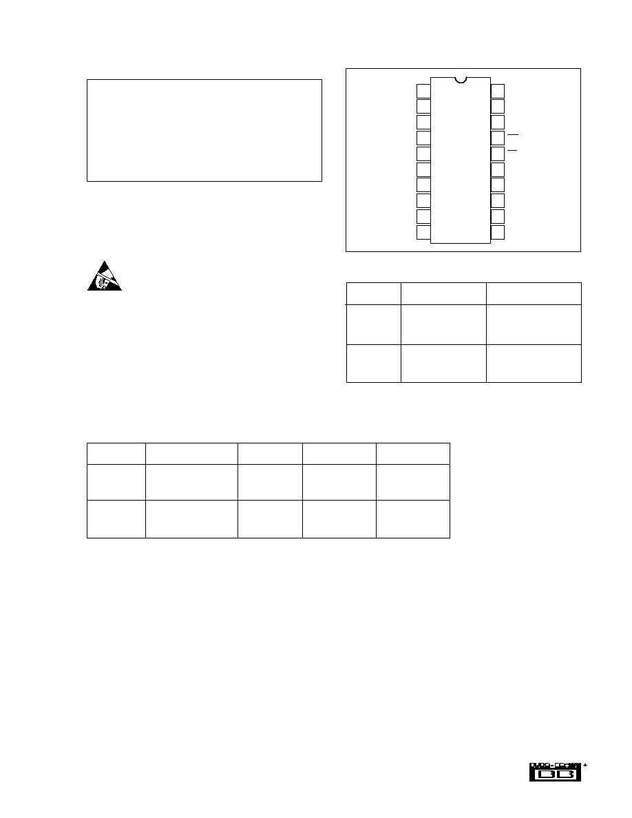
PACKAGE DRAWING
PRODUCT
PACKAGE
NUMBER
(1)
DAC7545JP
20-Pin PDIP
222
DAC7545KP
20-Pin PDIP
222
DAC7545LP
20-Pin PDIP
222
DAC7545GLP
20-Pin PDIP
222
DAC7545JU
20-Pin SOIC
221
DAC7545KU
20-Pin SOIC
221
DAC7545LU
20-Pin SOIC
221
DAC7545GLU
20-Pin SOIC
221
NOTE: (1) For detailed drawing and dimension table, please see end of data
sheet, or Appendix C of Burr-Brown IC Data Book.
ABSOLUTE MAXIMUM RATINGS
(1)
T
A
= +25
°
C, unless otherwise noted.
V
DD
to DGND ........................................................................... 0.3V, +17
Digital Input to DGND ............................................................... 0.3V, V
DD
V
RFB
, V
REF
, to DGND ........................................................................
±
25V
V
PIN 1
to DGND ......................................................................... 0.3V, V
DD
AGND to DGND ........................................................................ 0.3V, V
DD
Power Dissipation: Any Package to +75
°
C .................................... 450mW
Derates above +75
°
C by ................................ 6mW/
°
C
Operating Temperature:
Commercial J, K, L, GL .................................................. 40
°
C to +85
°
C
Storage Temperature ...................................................... 65
°
C to +150
°
C
Lead Temperature (soldering, 10s) ................................................ +300
°
C
NOTE: (1) Stresses above those listed above may cause permanent damage to
the device. This is a stress rating only and functional operation of the device at
these or any other condition above those indicated in the operational sections of
this specification is not implied. Exposure to absolute maximum rating conditions
for extended periods may affect device reliability.
PIN CONNECTIONS
ELECTROSTATIC
DISCHARGE SENSITIVITY
Any integral circuit can be damaged by ESD. Burr-Brown
recommends that all integrated circuits be handled with
appropriate precautions. Failure to observe proper handling
and installation procedures can cause damage.
ESD damage can range from subtle performance degrada-
tion to complete device failure. Precision integrated circuits
may be more susceptible to damage because very small
parametric changes could cause the device not to meet
published specifications.
PACKAGE INFORMATION
DAC7545
1
2
3
4
5
6
7
8
9
10
20
19
18
17
16
15
14
13
12
11
OUT 1
AGND
DGND
(MSB) DB
11
DB
10
DB
9
DB
8
DB
7
DB
6
DB
5
R
FB
V
REF
V
DD
WR
CS
DB
0
(LSB)
DB
1
DB
2
DB
3
DB
4
ORDERING INFORMATION
Top View
DIP/SOIC
4
DAC7545
PAD
FUNCTION
1
OUT 1
2
AGND
3
AGND
4
DGND
5
DB11
6
DB10
7
DB9
8
DB8
9
DB7
10
DB6
11
DB
5
12
DB
4
13
DB
3
14
DB
2
15
DB
1
(LSB)
16
DB
0
17
CS
18
WR
19
XYR
20
V
DD
21
V
REF
22
R
FB
23
OUT
1
WRITE CYCLE TIMING DIAGRAM
Mode Selection
Write Mode
Hold Mode
CS and WR low, DAC responds
Either CS or WR high, data bus
to Data Bus (DB
0
-DB
11
) inputs.
(DB
0
-DB
11
) is locked out; DAC
holds last data present when
WR or CS assumed high state.
NOTES: V
DD
= +5V, t
R
= t
F
= 20ns. V
DD
= +15V, t
R
= t
F
= 40ns. All inputs signal
rise and fall times measured from 10% to 90% of V
DD
. Timing measurement
reference level is (V
IH
+ V
IL
)/2.
t
DS
t
DH
V
IH
V
IL
Data
Valid
V
DD
0
t
WR
t
CS
t
CH
V
DD
0
V
DD
0
Data In
(DB
0
-DB
11
)
WR
CS
PAD
FUNCTION
Substrate Bias: Isolated. NC: No Connection
MECHANICAL INFORMATION
MILS (0.001")
MILLIMETERS
Die Size
136 x 134
±
5
3.45 x 3.40
±
0.13
Die Thickness
20
±
3
0.51
±
0.08
Min. Pad Size
4 x 4
0.10 x 0.10
Metalization
Aluminum
DAC7545 DIE TOPOGRAPHY
23
22
DISCUSSION
OF SPECIFICATIONS
Relative Accuracy
This term (also known as end point linearity) describes the
transfer function of analog output to digital input code.
Relative accuracy describes the deviation from a straight
line after zero and full scale have been adjusted.
Differential Nonlinearity
Differential nonlinearity is the deviation from an ideal 1LSB
change in the output, for adjacent input code changes. A
differential nonlinearity specification of 1LSB guarantees
monotonicity.
Gain Error
Gain error is the difference in measure of full-scale output
versus the ideal DAC output. The ideal output for the
DAC7545 is (4095/4096)(V
REF
). Gain error may be ad-
justed to zero using external trims as shown in the applica-
tions section.
Output Leakage Current
The current which appears at OUT 1 with the DAC loaded
with all zeros.
Multiplying Feedthrough Error
The AC output error due to capacitive feedthrough from
V
REF
to OUT 1 with the DAC loaded with all zeros. This test
is performed using a 10kHz sine wave.
Output Current Settling Time
The time required for the output to settle within
±
0.5LSB
of final value from a change in code of all zeros to all ones,
or all ones to all zeros.
5
DAC7545
Propagation Delay
The delay of the internal circuitry is measured as the time
from a digital code change to the point at which the
output reaches 90% of final value.
Digital-to-Analog Glitch Impulse
The area of the glitch energy measured in nanovolt-seconds.
Key contributions to glitch energy are internal circuitry
timing differences and charge injected from digital
logic. The measurement is performed with V
REF
= GND and
an OPA600 as the output op amp and G
1
(phase
compensation) = 0pF.
Monotonicity
Monotonicity assures that the analog output will increase
or stay the same for increasing digital input codes. The
DAC7545 is guaranteed monotonic to 12 bits, except the
J grade is specified to be 10-bit monotonic.
Power Supply Rejection
Power supply rejection is the measure of the sensitivity of
the output (full scale) to a change in the power supply
voltage.
CIRCUIT DESCRIPTION
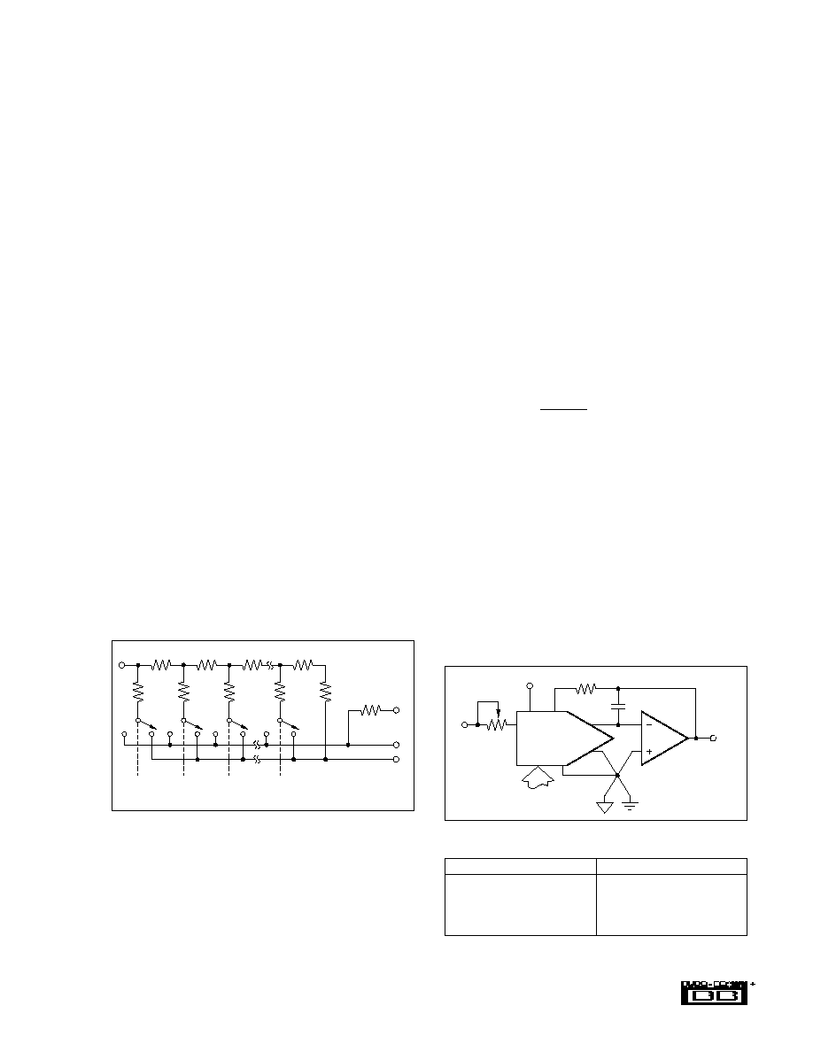
Figure 1 shows a simplified schematic of the digital-to-
analog converter portion of the DAC7545. The current from
the V
REF
pin is switched from OUT 1 to AGND by the
FET switch. This circuit architecture keeps the resistance at
the reference pin constant and equal to R
LDR
, so the reference
could be provided by either a voltage or current, AC or DC,
positive or negative polarity, and have a voltage range up to
±
20V even with V
DD
= 5V. The R
LDR
is equal to "R" and is
typically 11k
.
FIGURE 2. Unipolar Binary Operation.
BINARY CODE
ANALOG OUTPUT
MSB
LSB
1111 1111 1111
V
IN
(4095/4096)
1000 0000 0000
V
IN
(2048/4096) = 1/2V
IN
0000 0000 0001
V
IN
(1/4096)
0000 0000 0000
0 V
TABLE I. Unipolar Codes.
The output capacitance of the DAC7545 is code dependent
and varies from a minimum value (70pF) at code 000H to a
maximum (200pF) at code FFFH.
The input buffers are CMOS inverters, designed so that
when the DAC7545 is operated from a 5V supply (V
DD
), the
logic threshold is TTL-compatible. Being simple CMOS
inverters, there is a range of operation where the inverters
operate in the linear region and thus draw more supply
FIGURE 1. Simplified DAC Circuit of the DAC7545.
R
R
2R
2R
R
2R
R
2R
R
FB
2R
OUT 1
AGND
DB0
(LSB)
DB9
DB10
DB11
(MSB)
V
REF
OPA604
V
IN
R
1
R
2
V
DD
R
FB
DAC7545
AGND
DGND
OUT 1
DB
0
-DB
11
C
1
33pF
+5V
V
OUT
V
REF
current than normal. Minimizing this transition time through
the linear region and insuring that the digital inputs are
operated as close to the rails as possible will minimize the
supply drain current.
APPLICATIONS
UNIPOLAR OPERATION
Figure 2 shows the DAC7545 connected for unipolar opera-
tion. The high-grade DAC7545 is specified for a 1LSB gain
error, so gain adjust is typically not needed. However, the
resistors shown are for adjusting full-scale errors. The value
of R
1
should be minimized to reduce the effects of mis-
matching temperature coefficients between the internal and
external resistors. A range of adjustment of 1.5 times the
desired range will be adequate. For example, for a
DAC7545JP, the gain error is specified to be
±
25LSB. A
range of adjustment of
±
37LSB will be adequate. The
equation below results in a value of 458
for the potentiom-
eter (use 500
).
R
1
= (3
x
Gain Error)
R
LADDER
4096
The addition of R
1
will cause a negative gain error. To
compensate for this error, R
2
must be added. The value of R
2
should be one-third the value of R
1
.
The capacitor across the feedback resistor is used to com-
pensate for the phase shift due to stray capacitances of the
circuit board, the DAC output capacitance, and op amp input
capacitance. Eliminating this capacitor will result in exces-
sive ringing and an increase in glitch energy. This capacitor
should be as small as possible to minimize settling time.
The circuit of Figure 2 may be used with input voltages up
to
±
20V as long as the output amplifier is biased to handle
the excursions. Table I represents the analog output for four
codes into the DAC for Figure 2.