16-Bit, Voltage Output, Serial Input
DIGITAL-TO-ANALOG CONVERTER
DESCRIPTION
The DAC7731 is a 16-bit Digital-to-Analog Converter (DAC)
which provides 16 bits of monotonic performance over the
specified operating temperature range and offers a +10V
internal reference. Designed for automatic test equipment
and industrial process control applications, the DAC7731's
output swing can be configured in a
±
10V,
±
5V, or +10V
range. The flexibility of the output configuration allows the
DAC7731 to provide both unipolar and bipolar operation by
pin strapping. The DAC7731 includes a high-speed output
amplifier with a maximum settling time of 5
µ
s to
±
0.003%
FSR for a 20V full-scale change and only consumes 100mW
(typical) of power.
The DAC7731 features a standard 3-wire, SPI-compatible
serial interface with double buffering to allow asynchronous
updates of the analog output as well as a serial data output
line for daisy-chaining multiple DAC7731's. A user program-
mable reset control forces the DAC output to either min-scale
(0000
H
) or mid-scale (8000
H
), overriding both the input and
DAC register values. The DAC7731 is available in a
SSOP-24 package and three performance grades specified
to operate from ≠40
∞
C to +85
∞
C.
FEATURES
q
LOW POWER: 150mW MAXIMUM
q
+10V INTERNAL REFERENCE
q
UNIPOLAR OR BIPOLAR OPERATION
q
SETTLING TIME: 5
µ
s to
±
0.003% FSR
q
16-BIT MONOTINICITY, ≠40
∞
C TO +85
∞
C
q
±
10V,
±
5V, OR +10V CONFIGURABLE VOLTAGE
OUTPUT
q
RESET TO ZERO OR MID-SCALE
q
DOUBLE-BUFFERED DATA INPUT
q
DAISY-CHAIN FEATURE FOR MULTIPLE
DAC7731s ON A SINGLE BUS
q
SMALL SSOP-24 PACKAGE
APPLICATIONS
q
PROCESS CONTROL
q
ATE PIN ELECTRONICS
q
CLOSED-LOOP SERVO CONTROL
q
MOTOR CONTROL
q
DATA ACQUISITION SYSTEMS
DAC7731
SBAS249 ≠ DECEMBER 2001
www.ti.com
Copyright © 2001, Texas Instruments Incorporated
Please be aware that an important notice concerning availability, standard warranty, and use in critical applications of
Texas Instruments semiconductor products and disclaimers thereto appears at the end of this data sheet.
Buffer
+10V
Reference
Control
Logic
Enable
Input
Register
DAC
Register
DAC
REFEN
RSTSEL
RST
LDAC
SCLK
CS
SDO
SDI
V
DD
V
SS
V
CC
REFADJ
REF
OUT
REF
IN
V
REF
R
OFFSET
RFB2
RFB1
SJ
V
OUT
AGND
DGND
DAC7731
PRODUCTION DATA information is current as of publication date.
Products conform to specifications per the terms of Texas Instruments
standard warranty. Production processing does not necessarily include
testing of all parameters.
DAC7731
2
SBAS249
www.ti.com
ABSOLUTE MAXIMUM RATINGS
(1)
V
CC
to V
SS
........................................................................... ≠0.3V to +32V
V
CC
to AGND ...................................................................... ≠0.3V to +16V
V
SS
to AGND ...................................................................... ≠16V to +0.3V
AGND
to DGND ................................................................... ≠0.3V to 0.3V
REF
IN
to AGND .............................................................. 0V to V
CC
≠ 1.4V
V
DD
to DGND ........................................................................ ≠0.3V to +6V
Digital Input Voltage to DGND ................................. ≠0.3V to V
DD
+ 0.3V
Digital Output Voltage to DGND .............................. ≠0.3V to V
DD
+ 0.3V
Operating Temperature Range ........................................ ≠40
∞
C to +85
∞
C
Storage Temperature Range ......................................... ≠65
∞
C to +150
∞
C
Junction Temperature (TJ Max) .................................................... +150
∞
C
NOTE: (1) Stresses above those listed under "Absolute Maximum Ratings"
may cause permanent damage to the device. Exposure to absolute maximum
conditions for extended periods may affect device reliability.
ELECTROSTATIC
DISCHARGE SENSITIVITY
This integrated circuit can be damaged by ESD. Texas Instru-
ments recommends that all integrated circuits be handled with
appropriate precautions. Failure to observe proper handling
and installation procedures can cause damage.
ESD damage can range from subtle performance degradation
to complete device failure. Precision integrated circuits may be
more susceptible to damage because very small parametric
changes could cause the device not to meet its published
specifications.
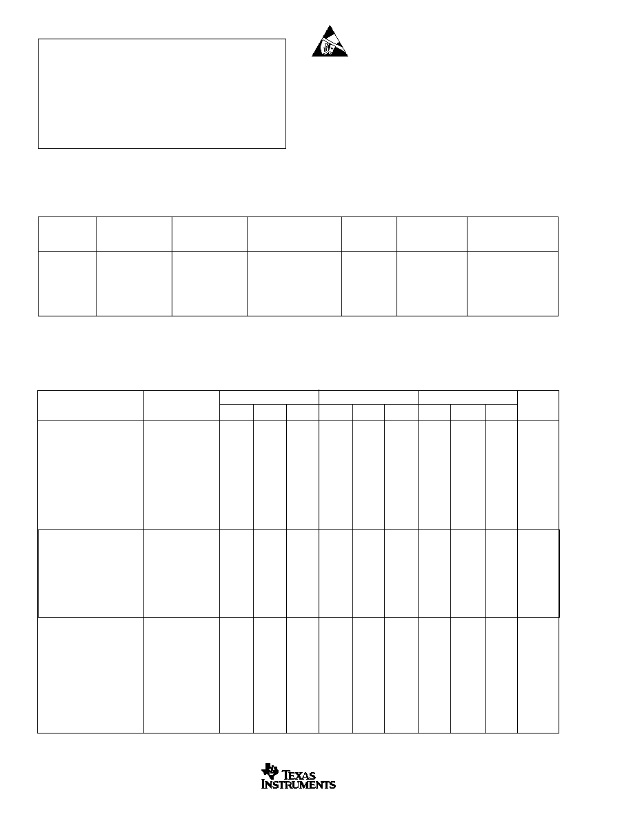
PACKAGE/ORDERING INFORMATION
SPECIFIED
PACKAGE
TEMPERATURE
PACKAGE
ORDERING
TRANSPORT
PRODUCT
PACKAGE-LEAD
DESIGNATOR
(1)
RANGE
MARKING
NUMBER
(2)
MEDIA, QUANTITY
DAC7731E
SSOP-24
DB
≠40
∞
C to +85
∞
C
DAC7731E
DAC7731E
Rails, 60
"
"
"
"
"
DAC7731E/1K
Tape and Reel,1000
DAC7731EB
SSOP-24
DB
≠40
∞
C to +85
∞
C
DAC7731EB
DAC7731EB
Rails, 60
"
"
"
"
"
DAC7731EB/1K
Tape and Reel, 1000
DAC7731EC
SSOP-24
DB
≠40
∞
C to +85
∞
C
DAC7731EC
DAC7731EC
Rails, 60
"
"
"
"
"
DAC7731EC/1K
Tape and Reel, 1000
NOTE: (1) For the most current specifications and package information, refer to our web site at www.ti.com. (2) Models with a slash (/) are available only in Tape and
Reel in the quantities indicated (e.g., /1K indicates 1000 devices per reel). Ordering 1000 pieces of "DAC7731EC/1K" will get a single 1000-piece Tape and Reel.
DAC7731E
DAC7731EB
DAC7731EC
PARAMETER
CONDITIONS
MIN
TYP
MAX
MIN
TYP
MAX
MIN
TYP
MAX
UNITS
ACCURACY
Linearity Error (INL)
±
6
±
4
±
3
LSB
T
A
= 25
∞
C
±
5
±
3
±
2
LSB
Differential Linearity Error (DNL)
±
4
±
2
±
1
LSB
Monotonicity
14
15
16
Bits
Offset Error
±
0.1
% of FSR
Offset Error Drift
±
2
ppm/
∞
C
Gain Error
With Internal REF
±
0.4
±
0.25
±
0.15
% of FSR
With External REF
±
0.25
±
0.1
% of FSR
Gain Error Drift
With Internal REF
±
15
±
10
±
7
ppm/
∞
C
PSRR (V
CC
or V
SS
)
At Full-Scale
50
200
ppm/V
ANALOG OUTPUT
(1)
Voltage Output
(2)
+11.4/≠4.75
0 to 10
V
+11.4/≠11.4
±
10
V
+11.4/≠6.4
±
5
V
Output Current
±
5
mA
Output Impeadance
0.1
Maximum Load Capacitance
200
pF
Short-Circuit Current
±
15
mA
Short-Circuit Duration
AGND
Indefinite
REFERENCE
Reference Output
9.96
10
10.04
9.975
10.025
V
REF
OUT
Impedance
400
REF
OUT
Voltage Drift
±
15
±
10
±
7
ppm/
∞
C
REF
OUT
Voltage Adjustment
(3)
±
25
mV
REF
IN
Input Range
(4)
4.75
V
CC
≠ 1.4
V
REF
IN
Input Current
10
nA
REFADJ Input Range
Absolute Max Value that
0
10
V
can be applied is V
CC
REFADJ Input Impedance
50
k
V
REF
Output Current
≠2
+2
mA
V
REF
Impedance
1
ELECTRICAL CHARACTERISTICS
All specifications at T
A
= T
MIN
to T
MAX
, V
CC
= +15V, V
SS
= ≠15V, V
DD
= +5V, Internal refi/ence enabled, unless otherwise noted.
DAC7731
3
SBAS249
www.ti.com
DYNAMIC PERFORMANCE
Settling Time to
±
0.003%
20V Output Step
3
5
µ
s
R
L
= 5k
, C
L
= 200pF,
with external REF
OUT
to REF
IN
filter
(5)
Digital Feedthrough
2
nV-s
Output Noise Voltage
at 10kHz
100
nV/
Hz
DIGITAL INPUT
V
IH
|I
H
| < 10
µ
A
0.7 ∑ V
DD
V
V
IL
|I
L
| < 10
µ
A
0.3 ∑ V
DD
V
DIGITAL OUTPUT
V
OH
I
OH
= ≠0.8mA
3.6
V
V
OL
I
OL
= 1.6mA
0.4
V
POWER SUPPLY
V
DD
+4.75
+5.0
+5.25
V
V
CC
+11.4
+15.75
V
V
SS
Bipolar Operation
≠15.75
≠11.4
V
Unipolar Opeation
≠15.75
≠4.75
V
I
DD
100
µ
A
I
CC
Unloaded
4
6
mA
I
SS
Unloaded
≠4
≠2.5
mA
Power
No Load, Ext. Reference
85
mW
No Load, Int. Reference
100
150
mW
TEMPERATURE RANGE
Specified Performance
≠40
+85
∞
C
Specifications same as grade to the left.
NOTES: (1) With minimum V
CC
/V
SS
requirements, internal reference enabled. (2) Please refer to the "Theory of Operation" section for more information with respect to output voltage
configurations. (3) See Figure 11 for gain and offset adjustment connection diagrams when using the internal reference. (4) The minimum value for REF
IN
must be equal to the greater
of V
SS
+14V and +4.75V, where +4.75V is the minimum voltage allowed. (5) Reference low-pass filter values: 100k
, 1.0
µ
F (see Figure 14).
ELECTRICAL CHARACTERISTICS
(Cont.)
All specifications at T
A
= T
MIN
to T
MAX
, V
CC
= +15V, V
SS
= ≠15V, V
DD
= +5V, Internal reference enabled, unless otherwise noted.
DAC7731E
DAC7731EB
DAC7731EC
PARAMETER
CONDITIONS
MIN
TYP
MAX
MIN
TYP
MAX
MIN
TYP
MAX
UNITS
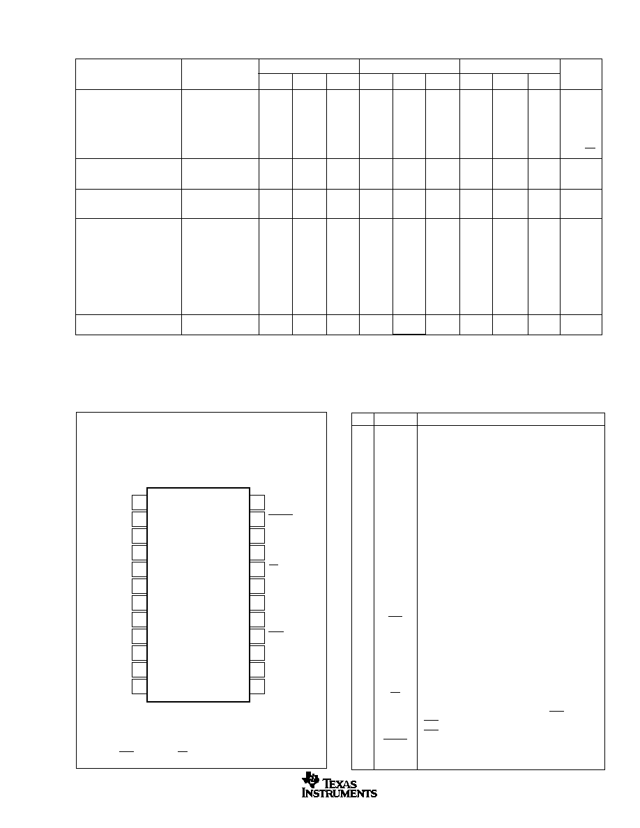
Top View
SSOP
PIN CONFIGURATION
PIN
NAME
DESCRIPTION
1
V
CC
Positive Analog Power Supply
2
REF
OUT
Internal Reference Output
3
REF
IN
Reference Input
4
REFADJ
Internal Reference Trim. (Acts as a gain adjustment
input when the internal reference is used.)
5
V
REF
Buffered Output from REF
IN
, can be used to drive
external devices. Internally, this pin directly drives the
DAC's circuitry.
6
R
OFFSET
Offsetting Resistor
7
AGND
Analog ground
8
RFB2
Feedback Resistor 2, used to configure DAC output
range.
9
RFB1
Feedback Resistor 1, used to configure DAC output
range.
10
SJ
Summing Junction of the Output Amplifier
11
V
OUT
DAC Voltage Output
12
V
DD
Digital Power Supply
13
DGND
Digital Ground
14
TEST
Reserved, Connect to DGND
15
NC
No Connection
16
RST
V
OUT
reset; active LOW, depending on the state of
RSTSEL, the DAC register is either reset to mid-
scale or min-scale.
17
LDAC
DAC register load control, rising dege triggered. Data
is loaded from the input register to the DAC register.
18
SDI
Serial Data Input. Data is latched into the input
register on the rising edge of SCLK.
19
SDO
Serial Data Output, delayed 16 SCLK clock cycles.
20
CS
Chip Select, Active LOW
21
SCLK
Serial Clock Input
22
RSTSEL
Reset Select; determines the action of RST. If HIGH,
RST will reset the DAC register to mid-scale. If LOW,
RST will reset the DAC register to min-scale.
23
REFEN
Enables internal +10V reference (REF
OUT
), active
LOW.
24
V
SS
Negative Analog Power Supply
PIN DESCRIPTIONS
V
CC
REF
OUT
REF
IN
REFADJ
V
REF
R
OFFSET
AGND
RFB2
RFB1
SJ
V
OUT
V
DD
V
SS
REFEN
RSTSEL
SCLK
CS
SDO
SDI
LDAC
RST
NC
TEST
DGND
1
2
3
4
5
6
7
8
9
10
11
12
24
23
22
21
20
19
18
17
16
15
14
13
DAC7731
NOTE: (1) RST, LDAC, SDI, CS and SCK are Schmitt-triggered inputs.
DAC7731
4
SBAS249
www.ti.com
PARAMETER
DESCRIPTION
MIN
TYP
MAX
UNITS
t
WH
SCLK HIGH Time
25
ns
t
WL
SCLK LOW Time
25
ns
t
SDI
Setup Time: Data in valid before rising SCLK
5
ns
t
HDI
Hold Time: Data in valid after rising SCLK
20
ns
t
SCS
Setup Time: CS falling edge before first rising SCLK
15
ns
t
HSC
Hold Time: CS rising edge after 16th rising SCLK
0
ns
t
DDO
Delay Time: CS Falling Edge to Data Out valid, C
L
= 20pF on SDO
50
ns
t
HDO
Hold Time: Data Out valid after SCLK rising edge, C
L
20pF on SDO
50
ns
t
DDOZ
Delay Time: CS rising edge to SDO = High Impedance
70
ns
t
WCSH
CS HIGH Time
50
ns
t
WLDL
LDAC LOW Time
20
ns
t
WLDH
LDAC HIGH Time
20
ns
t
SLD
Setup Time: 16th Rising SCLK Before LDAC Rising Edge
15
ns
t
DLD
Delay Time: LDAC rising edge to first SCLK rising edge of next
15
ns
transfer cycle.
t
SCLK
Setup Time: CS High before falling SCLK edge following 16th
5
ns
rising SCLK edge
t
SRS
Setup Time: RSTSEL Valid Before RST LOW
0
ns
t
HRS
Hold Time: RSTSEL valid after RST HIGH
20
ns
t
WRL
RST LOW Time
30
ns
t
S
DAC V
OUT
Settling Time
5
µ
s
TIMING CHARACTERISTICS
V
CC
= +15V, V
SS
= ≠15V, V
DD
= 5V; R
L
= 2k
to AGND; C
L
= 200pF to AGND; all specifications ≠40
∞
C to +85
∞
C, unless otherwise noted.
DAC7731
CS
SCLK
SDI
SDO
LDAC
V
OUT
t
SCS
t
HCS
t
WH
t
WL
t
SCLK
t
HDI
t
SDI
t
DDO
t
HDO
t
DDOZ
t
WLDL
t
DLD
t
SLD
t
S
t
WLDH
t
WCSH
1
2
16
B15
B14
B13
B0
A15
A14
A13
A0
C15
C14
C13
C12
B15
B14
B13
B12
Word B
Word A
Word C
Word B
±
0.003% of FSR
Error Bands
RSTSEL
(RSTSEL = LOW)
(RSTSEL = HIGH)
RST
V
OUT
V
OUT
t
SRS
t
HRS
t
WRL
t
S
+FS
+FS
≠FS
≠FS
Min-Scale
Mid-Scale
INTERFACE TIMING
RESET TIMING
DAC7731
5
SBAS249
www.ti.com
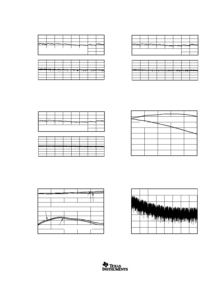
TYPICAL CHARACTERISTICS
T
A
= +25
∞
C (unless otherwise noted).
6
4
2
0
≠2
≠4
≠6
2.0
1.5
1.0
0.5
0.0
≠0.5
≠1.0
≠1.5
≠2.0
INL (LSB)
DNL (LSB)
LINEARITY ERROR AND DIFFERENTIAL
LINEARITY ERROR vs DIGITAL INPUT CODE
0000
H
2000
H
4000
H
6000
H
8000
H
Digital Input Code
A000
H
C000
H
E000
H
FFFF
H
Bipolar Configuration: V
OUT
= ≠10V to +10V
T
A
= 85
∞
C, Internal Reference Enabled
6
4
2
0
≠2
≠4
≠6
2.0
1.5
1.0
0.5
0.0
≠0.5
≠1.0
≠1.5
≠2.0
INL (LSB)
DNL (LSB)
LINEARITY ERROR AND DIFFERENTIAL
LINEARITY ERROR vs DIGITAL INPUT CODE
0000
H
2000
H
4000
H
6000
H
8000
H
Digital Input Code
A000
H
C000
H
E000
H
FFFF
H
Bipolar Configuration: V
OUT
= ≠10V to +10V
T
A
= 25
∞
C, Internal Reference Enabled
6
4
2
0
≠2
≠4
≠6
2.0
1.5
1.0
0.5
0.0
≠0.5
≠1.0
≠1.5
≠2.0
INL (LSB)
DNL (LSB)
LINEARITY ERROR AND DIFFERENTIAL
LINEARITY ERROR vs DIGITAL INPUT CODE
0000
H
2000
H
4000
H
6000
H
8000
H
Digital Input Code
A000
H
C000
H
E000
H
FFFF
H
Bipolar Configuration: V
OUT
= ≠10V to +10V
T
A
= ≠40
∞
C, Internal Reference Enabled
Ext. Ref, Unipolar Mode: V
OUT
= 0 to +10V
Int. Ref, Unipolar Mode: V
OUT
= 0 to +10V
Ext. Ref, Bipolar Mode: V
OUT
= ≠10 to +10V
Int. Ref, Bipolar Mode: V
OUT
= ≠10 to +10V
0.000
≠0.010
≠0.020
≠0.030
≠0.040
≠0.050
≠0.060
≠0.070
≠0.080
≠0.090
≠0.100
Error (%)
≠40
≠15
10
35
60
85
Temperature (
∞
C)
GAIN ERROR vs TEMPERATURE
Load = 200pF, 2k
4.4
4.3
4.2
4.1
4.0
3.9
3.8
3.7
I
CC
(mA)
0000
H
2000
H
4000
H
6000
H
8000
H
Digital Input Code
A000
H
C000
H
E000
H
FFFF
H
V
CC
SUPPLY CURRENT vs DIGITAL INPUT CODE
Bipolar Configuration: V
OUT
= ≠10V to +10V
Internal Reference Enabled, T
A
= 25
∞
C
1.00
0.75
0.50
0.25
0.00
≠0.25
≠0.50
≠0.75
≠1.00
Error (mV)
OFFSET ERROR vs TEMPERATURE
≠40
≠15
10
35
60
85
Temperature (
∞
C)
V
OUT
= 0 to +10V
V
OUT
= ≠10 to +10V
DAC7731
6
SBAS249
www.ti.com
TYPICAL CHARACTERISTICS
(Cont.)
T
A
= +25
∞
C (unless otherwise noted).
3.4
3.3
3.2
3.1
3.0
2.9
2.8
2.7
I
CC
(mA)
0000
H
2000
H
4000
H
6000
H
8000
H
Digital Input Code
A000
H
C000
H
E000
H
FFFF
H
V
CC
SUPPLY CURRENT vs DIGITAL INPUT CODE
Bipolar Configuration: V
OUT
= ≠10V to +10V
External Reference, REFEN = 5V, T
A
= 25
∞
C
≠1.50
≠1.75
≠2.00
≠2.25
≠2.50
≠2.75
I
SS
(mA)
0000
H
2000
H
4000
H
6000
H
8000
H
Digital Input Code
A000
H
C000
H
E000
H
FFFF
H
V
SS
SUPPLY CURRENT vs DIGITAL INPUT CODE
Bipolar Configuration: V
OUT
= ≠10V to +10V
T
A
= 25
∞
C
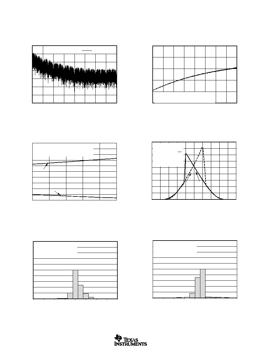
SUPPLY CURRENT vs TEMPERATURE
Load Current Excluded
V
CC
= +15V, V
SS
= ≠15V
Bipolar V
OUT
Configuration: ≠10V to +10V
I
CC
I
SS
7
6
5
4
3
2
1
0
≠1
≠2
≠3
I
CC
, I
SS
(mA)
≠40
≠15
10
35
60
85
Temperature (
∞
C)
1800
1600
1400
1200
1000
800
600
400
200
0
I
DD
(
µ
A)
0.0
0.5
1.0
1.5
2.0
2.5
3.0
3.5
4.0
4.5
5.0
V
LOGIC
(V)
SUPPLY CURRENT vs LOGIC INPUT VOLTAGE
T
A
= 25
∞
C, Transition
Shown for a Single
Input (Applies to CS,
SCLK,D
IN
and LDAC
inputs)
100
90
80
70
60
50
40
30
20
10
0
Frequency
HISTOGRAM OF V
CC
CURRENT CONSUMPTION
3.000
3.500
4.000
4.500
5.000
I
CC
(mA)
Bipolar Output Configuration
Internal Reference Enabled
Code = 5555
H
100
90
80
70
60
50
40
30
20
10
0
Frequency
HISTOGRAM OF V
SS
CURRENT CONSUMPTION
≠3.50
≠3.00
≠2.50
≠2.00
≠1.50
I
SS
(mA)
Bipolar Output Configuration
Internal Reference Enabled
Code = 5555
H
DAC7731
7
SBAS249
www.ti.com
TYPICAL CHARACTERISTICS
(Cont.)
T
A
= +25
∞
C (unless otherwise noted).
10
0
≠10
≠20
≠30
≠40
≠50
≠60
≠70
≠80
PSRR (dB)
0.1K
1K
10K
100K
1M
10M
Frequency (Hz)
Bipolar Configuration:
±
10V V
OUT
Code 8000
H
≠V
SS
, V
CC
= 15V + 1Vp-p
V
DD
= 5V + 0.5Vp-p
V
SS
V
CC
V
DD
POWER-SUPPY REJECTION RATIO vs FREQUENCY
(Measured at V
OUT
)
10
0
≠10
≠20
≠30
≠40
≠50
≠60
≠70
≠80
PSRR (dB)
0.01K
0.1K
1K
10K
100K
1M
10M
POWER-SUPPY REJECTION RATIO vs FREQUENCY
(Measured at V
OUT
)
Frequency (Hz)
V
SS
V
CC
V
DD
Bipolar Configuration:
±
10V V
OUT
, Code FFFF
H
≠V
SS
, V
CC
= 15V + 1Vp-p, V
DD
= 5V + 0.5Vp-p
INTERNAL REFERENCE START-UP
V
CC
(5V/div)
REF
OUT
(2V/div)
Time (2ms/div)
0V
15V
0V
10V
10.015
10.010
10.005
10.000
9.995
9.990
9.985
REF
OUT
(V)
≠40
≠15
10
35
60
85
Temperature (
∞
C)
INTERNAL REFERENCE OUTPUT vs TEMPERATURE
Source
Sink
OUTPUT VOLTAGE vs R
LOAD
12
8
4
0
≠4
≠8
≠12
V
OUT
(V)
0.0
0.1
1.0
10.0
100.0
R
LOAD
(k
)
Loaded to V
CC
V
CC
= +15V
Loaded to AGND
11.0
10.5
10.0
9.5
9.0
8.5
REF
OUT
(V)
REF
OUT
LOAD(k
)
REF
OUT
VOLTAGE vs LOAD
1
10
100
1K
DAC7731
8
SBAS249
www.ti.com
TYPICAL CHARACTERISTICS
(Cont.)
T
A
= +25
∞
C (unless otherwise noted).
900
800
700
600
500
400
300
200
100
0
Output Noise (nV/Hz)
0.01K
0.1K
1K
10K
100K
1M
10M
OUTPUT NOISE vs FREQUENCY
Frequency (Hz)
Unipolar Configuration, Internal Reference Enabled
Code FFFF
H
Code 0000
H
800
700
600
500
400
300
200
100
0
Output Noise (nV/rtHz)
0.01K
0.1K
1K
10K
100K
1M
10M
OUTPUT NOISE vs FREQUENCY
Frequency (Hz)
Bipolar Configuration:
±
10V, Internal Reference Enabled
Code 0000
H
Code FFFF
H
Code 8000
H
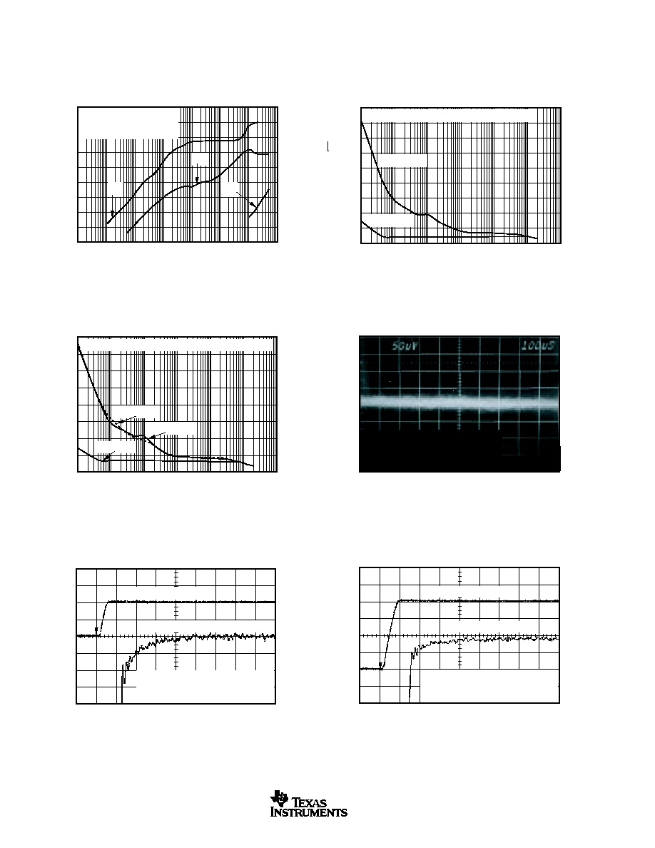
BROADBAND NOISE
V
OUT
(V, 50
µ
V/div)
Time (100
µ
s/div)
Internal Reference Enabled
Filtered with 1.6Hz Low-Pass
Code FFFF
H
, Bipolar
±
10V Configuration
10kHz Measurement BW
Unipolar Configuration: V
OUT
= 0 to +10V
Zero-Scale to +Full-Scale Change
5k
, 200pF Load
Large-Signal Output (5V/div)
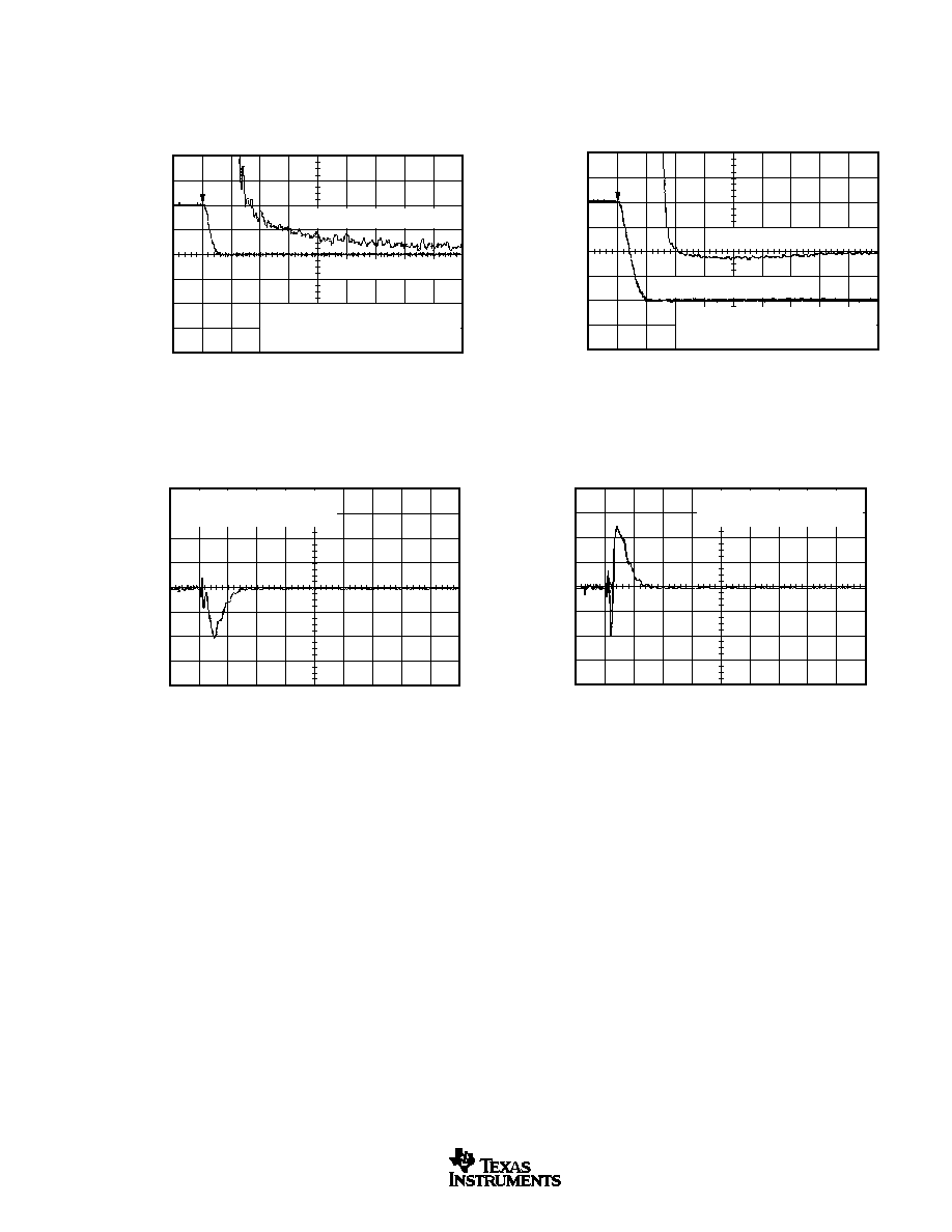
UNIPOLAR FULL-SCALE SETTLING TIME
Time (2
µ
s/div)
Small-Signal Error (150
µ
V/div)
Bipolar Configuration: V
OUT
= ≠10 to +10V
≠Full-Scale to +Full-Scale
5k
, 200pF Load
Large-Signal Output (5V/div)
BIPOLAR FULL-SCALE SETTLING TIME
Time (2
µ
s/div)
Small-Signal Error (300
µ
V/div)
10
0
≠10
≠20
≠30
≠40
≠50
≠60
≠70
≠80
PSRR (dB)
1
10
100
1K
10K
100K
1M
10M
POWER-SUPPY REJECTION RATIO vs FREQUENCY
(Measured at REF
OUT
)
Frequency (Hz)
V
SS
V
CC
V
DD
Internal Reference Enabled
≠V
SS
, V
CC
= 15V + 1Vp-p,
V
DD
= 5V + 0.5Vp-p
DAC7731
9
SBAS249
www.ti.com
TYPICAL CHARACTERISTICS
(Cont.)
T
A
= +25
∞
C (unless otherwise noted).
Unipolar Configuration: V
OUT
= 0V to +10V
+Full-Scale to Zero-Scale Change
5k
, 200pF Load
Large-Signal Output (5V/div)
UNIPOLAR FULL-SCALE SETTLING TIME
Time (2
µ
s/div)
Small-Signal Error (150
µ
V/div)
Bipolar Configuration: V
OUT
= ≠10 to +10V
+Full-Scale to ≠Full-Scale
5k
, 200pF Load
Large-Signal Output (5V/div)
BIPOLAR FULL-SCALE SETTLING TIME
Time (2
µ
s/div)
Small-Signal Error (300
µ
V/div)
Code 8000
H
to 7FFF
H
Bipolar Configuration:
±
10V V
OUT
MID-SCALE GLITCH
Time (1
µ
s/div)
V
OUT
(V, 100mV/div)
MID-SCALE GLITCH
Time (1
µ
s/div)
V
OUT
(V, 100mV/div)
Code 7FFF
H
to 8000
H
Bipolar Configuration:
±
10V V
OUT
DAC7731
10
SBAS249
www.ti.com
V
CC
REF
OUT
REF
IN
REFADJ
V
REF
R
OFFSET
AGND
RFB2
RFB1
SJ
V
OUT
V
DD
V
SS
REFEN
RSTSEL
SCLK
CS
SDO
SDI
LDAC
RST
NC
TEST
DGND
1
2
3
4
5
6
7
8
9
10
11
12
24
23
22
21
20
19
18
17
16
15
14
13
DAC7731
1
µ
F
0.1
µ
F
V
CC
1
µ
F
0.1
µ
F
V
DD
Control/Data
Bus
1
µ
F
0.1
µ
F
V
SS
(≠5V to +5V)
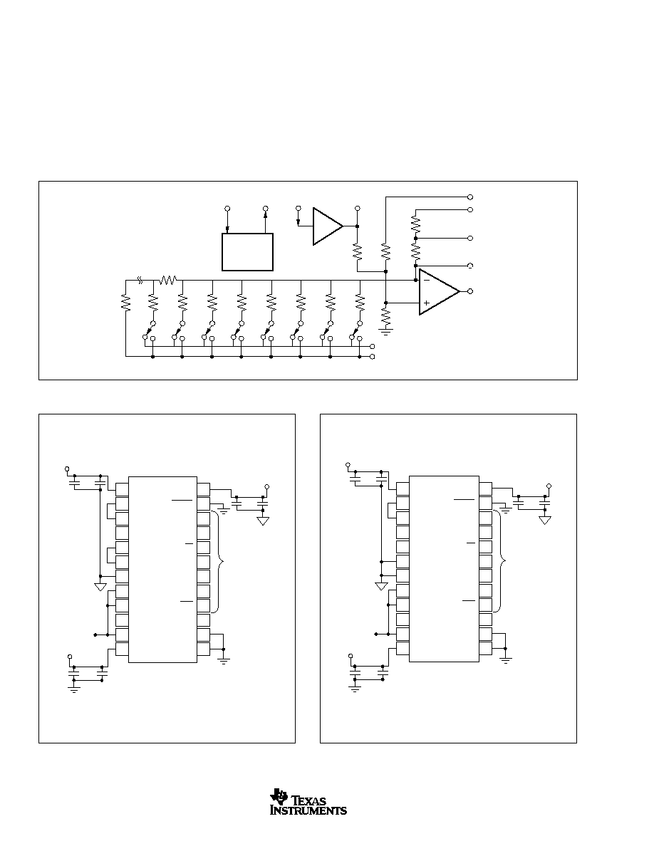
FIGURE 3. Basic Operation: V
OUT
= ≠5V to +5V.
THEORY OF OPERATION
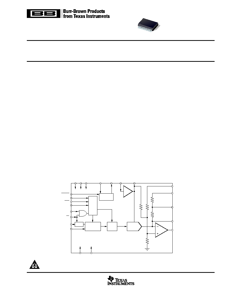
The DAC7731 is a voltage output, 16-bit DAC with a +10V
built-in internal reference. The architecture is an R-2R ladder
configuration with the three MSB's segmented, followed by
an operational amplifier that serves as a buffer, as shown in
Figure 1. The output buffer is designed to allow user-
configurable output adjustments giving the DAC7731 output
voltage ranges of 0V to +10V, ≠5V to +5V, or ≠10V to +10V.
Please refer to Figures 2, 3, and 4 for pin configuration
information.
The digital input is a serial word made up of the DAC code
(MSB first) and is loaded into the DAC register using the
LDAC input pin. The converter can be powered from
±
12V
to
±
15V dual analog supplies and a +5V logic supply. The
device offers a reset function, which immediately sets the
DAC output voltage and DAC register to min-scale (code
0000
H
) or mid-scale (code 8000
H
). The data I/O and reset
functions are discussed in more detail in the following sec-
tions.
FIGURE 1. DAC7731 Architecture.
FIGURE 2. Basic Operation: V
OUT
= 0V to +10V.
2R
2R
2R
2R
2R
2R
2R
2R
2R
R/4
R/2
R/2
R/4
R/4
R
R
OFFSET
RFB2
RFB1
SJ
V
OUT
V
REF
V
REF
AGND
REF
IN
REF
ADJ
REF
OUT
+10V Internal
Reference
Buffer
V
CC
REF
OUT
REF
IN
REFADJ
V
REF
R
OFFSET
AGND
RFB2
RFB1
SJ
V
OUT
V
DD
V
SS
REFEN
RSTSEL
SCLK
CS
SDO
SDI
LDAC
RST
NC
TEST
DGND
1
2
3
4
5
6
7
8
9
10
11
12
24
23
22
21
20
19
18
17
16
15
14
13
DAC7731
1
µ
F
0.1
µ
F
V
CC
1
µ
F
0.1
µ
F
V
DD
Control/Data
Bus
1
µ
F
0.1
µ
F
V
SS
(0V to +10V)
DAC7731
11
SBAS249
www.ti.com
V
CC
REF
OUT
REF
IN
REFADJ
V
REF
R
OFFSET
AGND
RFB2
RFB1
SJ
V
OUT
V
DD
V
SS
REFEN
RSTSEL
SCLK
CS
SDO
SDI
LDAC
RST
NC
TEST
DGND
1
2
3
4
5
6
7
8
9
10
11
12
24
23
22
21
20
19
18
17
16
15
14
13
DAC7731
1
µ
F
0.1
µ
F
V
CC
1
µ
F
0.1
µ
F
V
DD
Control/Data
Bus
1
µ
F
0.1
µ
F
V
SS
(≠10V to +10V)
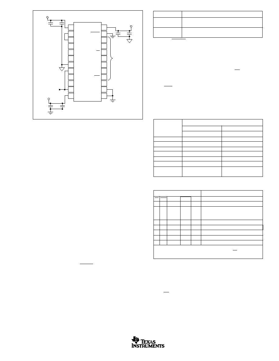
FIGURE 4. Basic Operation: V
OUT
= ≠10V to +10V.
ANALOG OUTPUTS
The output amplifier can swing to within 1.4V of the supply
rails, specified over the ≠40
∞
C to +85
∞
C temperature range.
This allows for a
±
10V DAC voltage output operation from
±
12V supplies with a typical 5% tolerance.
When the DAC7731 is configured for a unipolar, 0V to 10V
output, a negative voltage supply is required. This is due to
internal biasing of the output stage. Please refer to the
"Electrical Characteristics" table for more information.
The minimum and maximum voltage output values are de-
pendent upon the output configuration implemented and
reference voltage applied to the DAC7731. Please note that
V
SS
(the negative power supply) must be in the range of
≠4.75V to ≠15.75V for unipolar operation. The voltage on V
SS
sets several bias points within the converter and is required
in all modes of operation. If V
SS
is not in one of these two
configurations, the bias values may be in error and proper
operation of the device is not ensured.
REFERENCE INPUTS
The DAC7731 provides a built-in +10V voltage reference and
on-chip buffer to allow external component reference drive. To
use the internal reference, REFEN must be LOW, enabling the
reference circuitry of the DAC7731 (as shown in Table I) and
the REF
OUT
pin must be connected to REF
IN
. This is the input
to the on-chip reference buffer. The buffer's output is provided
at the V
REF
pin. In this configuration, V
REF
is used to setup the
DAC7731 output amplifier into one of three voltage output
modes as discussed earlier. V
REF
can also be used to drive
other system components requiring an external reference.
The internal reference of the DAC7731 can be disabled when
use of an external reference is desired. When using an
external reference, the reference input, REF
IN
, can be any
voltage between 4.75V (or V
SS
+ 14V, whichever is greater)
and V
CC
≠ 1.4V.
REFSEL
ACTION
1
Internal Reference disabled;
REF
OUT
= High Impedance
0
Internal Reference enabled;
REF
OUT
= +10V
TABLE I. REFEN Action.
DIGITAL INTERFACE
Table II shows the input data format for the DAC7731 and
Table III illustrates the basic control logic of the device. The
serial interface consists of a chip select input (CS), serial data
clock input (SCLK), serial data input (SDI), serial data output
(SDO), and load control input (LDAC). An asynchronous reset
input (RST), which is active LOW, is provided to simplify start-
up conditions, periodic resets, or emergency resets to a known
state, depending on the status of the reset select (RSTSEL)
signal. Please refer to the "DAC Reset" section for additional
information regarding the reset operation.
CONTROL STATUS
COMMAND
CS RST RSTSEL LDAC SCLK
ACTION
H
H
X
X
X
Shift Register is disabled on the serial bus.
Enable SDO pin from High Impedance;
L
H
X
X
X
enables shift operation and I/O bus
(SCLK, SDI, SDO).
L
H
X
X
Serial Data Shifted into Input Register
H
X
X
L
Serial Data Shifted into Input Register
(1)
X
H
X
X
Data in Input Register is Loaded into DAC Register.
X
L
H
X
X
Resets Input and DAC Registers to mid-scale.
X
L
L
X
X
Resets Input and DAC Registers to min-scale.
NOTE: (1) In order to avoid unwanted shifting of the input register by an
additional bit, care must be taken that a rising edge on CS only occurs
when SCLK is HIGH.
TABLE III. DAC7731 Logic Truth Table.
ANALOG OUTPUT
TABLE II. DAC7731 Data Format.
DIGITAL INPUT
Unipolar Configuration
Bipolar Configuration
Unipolar Straight Binary
Bipolar Offset Binary
0x0000
Zero (0V)
≠Full-Scale (≠V
REF
or ≠V
REF
/2)
0x0001
Zero + 1LSB
≠Full-Scale + 1LSB
:
:
:
0x8000
1/2 Full-Scale
Bipolar Zero
0x8001
1/2 Full-Scale + 1LSB
Bipolar Zero + 1LSB
:
:
:
0xFFFF
Full-Scale (V
REF
≠ 1LSB)
+Full-Scale (+V
REF
≠ 1LSB
or +V
REF
/2 ≠ 1LSB)
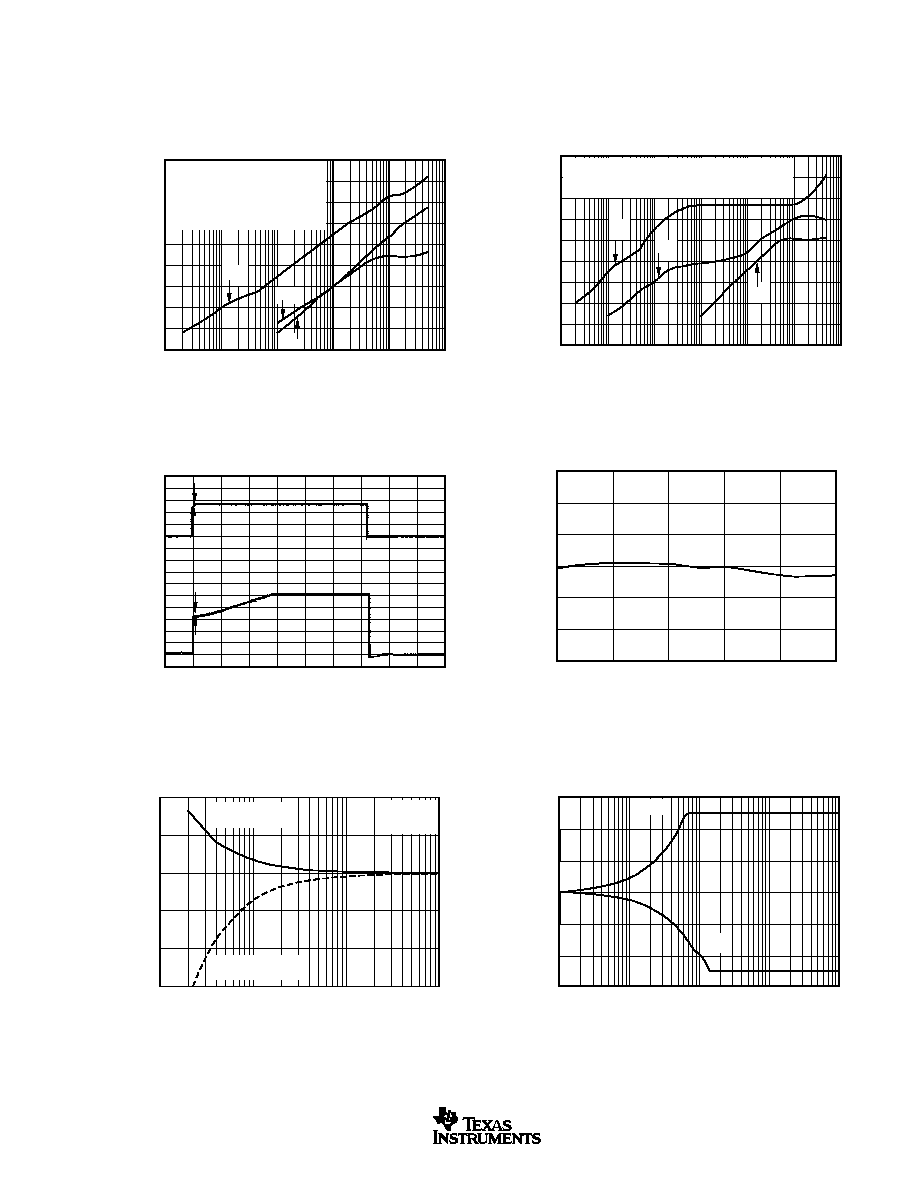
The DAC code is provided via a 16-bit serial interface, as shown
in Table II. The digital input word makes up the digital code to
be loaded into the data input register of the device. A typical
data transfer and DAC output update takes place as follows:
Once CS is active (LOW), the DAC7731 is enabled on the serial
bus and the 16-bit serial data transfer can begin. The serial data
is shifted into the device on each rising SCLK edge until all 16
bits are transferred (1 bit per 1 rising SCLK edge). Once
received, the data in the input register is loaded into the DAC
register upon reception of a rising edge on the LDAC input (load
command). This action updates the analog output, V
OUT
, to the
desired voltage specified by the digital input word. A rising edge
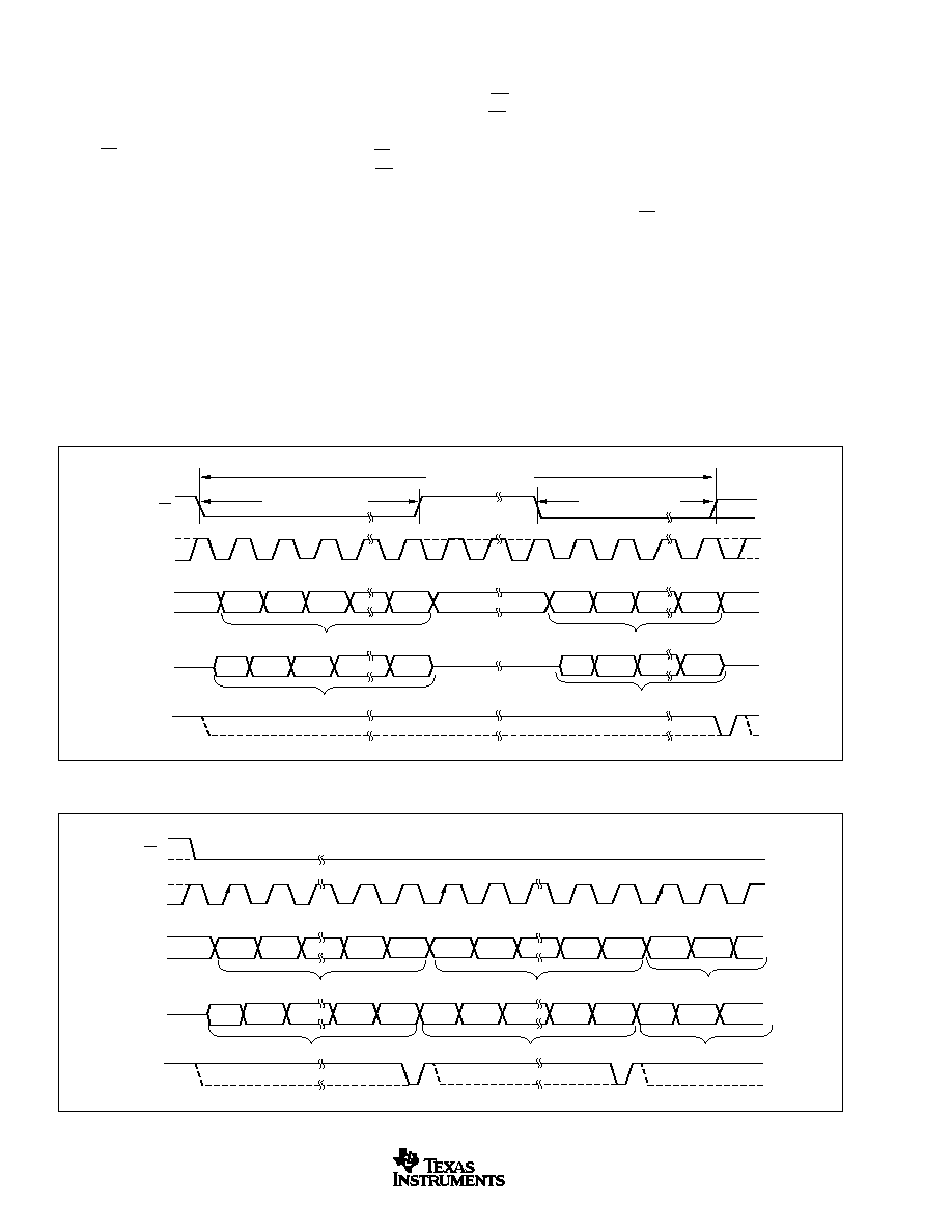
DAC7731
12
SBAS249
www.ti.com
on LDAC is completely asynchronous to the serial interface of
the device and can occur at any time. Care must be taken to
ensure that the entire 16 bits of data are loaded into the input
register before issuing a LDAC active edge. Additional load
commands will have no effect on the DAC output if the data in
the input register is unchanged between rising LDAC edges.
When CS is returned HIGH, the rising edge on CS must
occur when SCLK is HIGH. Application of a rising CS edge
when SCLK is LOW will cause one additional shift in the
serial input shift register, corrupting the desired input data.
TIMING CONSIDERATIONS
The flexible interface of the DAC7731 can operate under a
number of different scenarios as is required by a host
controller. Critical timing for a 16-bit data transfer cycle is
shown in the Interface Timing section of the Timing Charac-
teristics. While this is the most common method of writing to
the DAC7731, the device accepts two additional modes of
data transfer from the host. These are byte transfer mode
and continuous transfer mode.
Byte transfer mode is especially useful when an 8-bit host is
communicating with the DAC. Data transfer can occur with-
out requiring an additional general purpose I/O pin to control
the CS input of the DAC in cycles of 16 clocks. A HIGH state
on CS stops data from coming into and out of the internal
shift register. This provides byte-wide support for 8-bit host
processors. Figure 5 is an example of the timing cycle of
such a data transfer.
The remaining data transfer mode accepted by the DAC7731
is continuous transfer. The CS of the DAC7731 can be tied
LOW or held LOW by the controller for an indefinite number of
serial clock cycles. Each clock cycle will transfer data into the
DAC via SDI and out of the DAC on SDO. Care must be taken
that the LDAC signal to the DAC(s) is timed correctly so that
valid data is transferred into the DAC register on each rising
LDAC edge. ("Valid data" refers to the serial data latched on
each of the 16 rising SCLK edges prior to the occurrence of a
rising LDAC signal.) The rising edge of LDAC must occur
before the first rising SCLK edge of the following 16-bit
transfer. Figure 6 shows continuous transfer timing.
16-Bit Data Word
Most Significant Byte
Least Significant Byte
Byte 1, Word N
Byte 2, Word N
Byte 1, Word N ≠ 1
Byte 2, Word N ≠ 1
B15
A15
A14
A13
A8
A7
A6
A0
B14
B13
B8
B7
B6
B0
1
2
8
9
10
16
CS
SCLK
SDI
SDO
LDAC
1
2
16
1
2
16
1
2
B15
B14
B1
B0
C15
C14
C1
C0
D15
D14
C14
C15
B0
B1
B14
B15
A0
A1
A14
A15
Word N
Word N + 1
Word N + 2
Word N ≠ 1
Word N
Word N + 1
CS
SCLK
SDI
SDO
LDAC
FIGURE 6. Continuous Transfer Control.
FIGURE 5. Byte-Wide Data Write Cycle.
DAC7731
13
SBAS249
www.ti.com
V
CC
REF
OUT
REF
IN
REFADJ
V
REF
R
OFFSET
AGND
RFB2
RFB1
SJ
V
OUT
V
DD
V
SS
REFEN
RSTSEL
SCLK
CS
SDO
SDI
LDAC
RST
NC
TEST
DGND
1
2
3
4
5
6
7
8
9
10
11
12
24
23
22
21
20
19
18
17
16
15
14
13
DAC7731
V
CC
REF
OUT
REF
IN
REFADJ
V
REF
R
OFFSET
AGND
RFB2
RFB1
SJ
V
OUT
V
DD
V
SS
REFEN
RSTSEL
SCLK
CS
SDO
SDI
LDAC
RST
NC
TEST
DGND
1
2
3
4
5
6
7
8
9
10
11
12
24
23
22
21
20
19
18
17
16
15
14
13
DAC7731
From Host
Controller
To next
DAC7731
First Device in Chain
Second Device in Chain
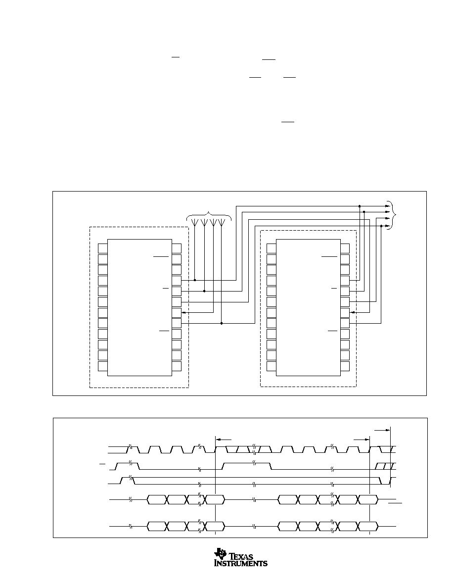
FIGURE 7. DAC7731 Daisy-Chain Schematic.
DAC7731's in a daisy-chained configuration, as shown in
Figure 7.
DAC RESET
The RST and RSTSEL inputs control the reset of the analog
output. The reset command is level triggered by a low signal on
RST. Once RST is LOW, the DAC output will begin settling to
the mid-scale or min-scale code depending on the state of the
RSTSEL input. A HIGH value on RSTSEL will cause V
OUT
to
reset to the mid-scale code (8000
H
) and a LOW value will reset
V
OUT
to min-scale (8000
H
). A change in the state of the RSTSEL
input while RST is LOW will cause a corresponding change in
the reset command selected internally and consequently change
the output value of V
OUT
of the DAC. Note that a valid reset
signal also resets the input register of the DAC to the value
specified by the state of RSTSEL.
SCLK
CS
LDAC
SDI
A15
A14
A0
X
X
X
SDO
1
2
1
2
16
16
LSBs latched
LSBs latched
Both DAC V
OUT
's
are updated
First Data Transfer Cycle
Previous cycle word from host
(to DAC7731 B SDI)
B15
B14
B1
B0
A15
A14
A1
A0
FIGURE 8. DAC7731 Daisy-Chain Timing for Figure 7.
DAISY-CHAINING USING SDO
Multiple DAC7731's can be connected to a single serial port
by attaching each of their control inputs in parallel and daisy-
chaining the SDO and SDI I/O's of each device. The SDO
output of the DAC7731 is active when CS is LOW and can
be left unconnected when not required for use in a daisy-
chain configuration.
Once a data transfer cycle begins, new data is shifted into SDI
and data currently residing in the shift register (from previous
cycle, power-up, or reset command) is presented on SDO, MSB
first. One data transfer cycle for each DAC7731 is required to
update all devices in the chain. The first data cycle written into
the chain will arrive at the last DAC7731 on the final cycle of the
data transfer. Upon completion of the required number of data
transfer cycles (one cycle per device), each DAC voltage output
is updated with a rising edge on the LDAC inputs.
Figure 8 shows the required timing to properly update two
DAC7731
14
SBAS249
www.ti.com
REFERENCE
OUTPUT
PIN STRAPPING
V
SJ
(1)
CONFIGURATION CONFIGURATION R
OFFSET
RFB1
RFB2
Internal
0V to +10V
to V
REF
to V
OUT
to V
OUT
+5V
Reference
≠10V to +10V
NC
NC
to V
OUT
+3.333V
≠5V to +5V
to AGND to V
OUT
to V
OUT
+1.666V
External
0V to V
REF
to V
REF
to V
OUT
to V
OUT
V
REF
/2
Reference
≠V
REF
to V
REF
NC
NC
to V
OUT
V
REF
/3
≠V
REF
/2 to V
REF
/2
to AGND to V
OUT
to V
OUT
V
REF
/6
NOTE: (1) Voltage measured at V
SJ
for a given configuration.
APPLICATIONS
GAIN AND OFFSET CALIBRATION
The architecture of the DAC7731 is designed in such a way
as to allow for easily configurable offset and gain calibration
using a minimum of external components. The DAC7731
has built-in feedback resistors and output amplifier summing
points brought out of the package in order to make the
absolute calibration possible. Figures 9 and 10 illustrate the
relationship of offset and gain adjustments for the DAC7731
in a unipolar configuration and in a bipolar configuration,
respectively.
should be at +10V ≠ 1LSB for the 0V to +10V or
±
10V output
range and +5V ≠ 1LSB for the
±
5V output range. Figure 11
shows the generalized external offset and gain adjustment
circuitry using potentiometers.
FIGURE 9. Relationship of Offset and Gain Adjustments for
V
OUT
= 0V to +10V Output Configuration.
Digital Input
H
Input =
FFFF
H
Input =
0000
Gain Adjust
Rotates
the Line
1LSB
+ Full Scale
Full Scale Range
Analog Output
(+V
REF
)
Zero Scale
(AGND)
Offset Adjust Translates the Line
FIGURE 10. Relationship of Offset and Gain Adjustments for
V
OUT
= ≠10V to +10V Output Configuration. (Same
Theory Applies for V
OUT
= ≠5V to +5V.)
Digital Input
Input =
0000
H
Gain
Adjust
Rotates
the Line
1LSB
Full Scale
Range
+ Full
Scale
≠ Full-Scale
(≠V
REF
OR ≠V
REF
/2)
Offset
Adjust
Translates
the Line
H
Input =
FFFF
Input = 8000
H
Analog Output
(+V
REF
or +V
REF
/2)
When calibrating the DAC's output, offset should be adjusted
first to avoid first order interaction of adjustments. In unipolar
mode, the DAC7731's offset is adjusted from code 0000
H
and for either bipolar mode, offset adjustments are made at
code 8000
H
. Gain adjustment can then be made at code
FFFF
H
for each configuration, where the output of the DAC
FIGURE 11. Generalized External Calibration Circuitry for
Gain and Symmetrical Offset Adjustment.
REF
ADJ
V
REF
R
OFFSET
AGND
RFB2
RFB1
SJ
4
5
6
7
8
9
10
DAC7731
Optional Gain
Adjust
Optional Offset
Adjust
R
1
R
POT2
R
POT1
R
S
V
OADJ
(Other Connections Omitted
for Clarity)
+
≠
I
SJ
OFFSET ADJUSTMENT
Offset adjustment is accomplished by introducing a small
current into the summing junction (SJ) of the DAC7731. The
voltage at SJ, or V
SJ
, is dependent on the output configura-
tion of the DAC7731. See Table IV for the required pin
strapping for a given configuration and the nominal values of
V
SJ
for each output range.
TABLE IV. Nominal V
SJ
versus V
OUT
and Reference Configu-
ration.
The current level required to adjust the DAC7731's offset can
be created by using a potentiometer divider as shown in
Figure 11 Another alternative is to use a unipolar DAC in order
to apply a voltage, V
OADJ
, to the resistor R
S
. A
±
2uA current
range applied to SJ will ensure offset adjustment coverage of
the
±
0.1% maximum offset specification of the DAC7731.
When in a unipolar configuration (V
SJ
= 5V), only a single
resistor, R
S
, is needed for symmetrical offset adjustment with
a 0V to 10V V
OADJ
range. When in one of the two bipolar
configurations, V
SJ
is either +3.333V (
±
10V range) or +1.666V
(
±
5V range), and circuit values chosen to match those given
in Table V will provide symmetrical offset adjust. Please refer
to Figure 11 for component configuration.
DAC7731
15
SBAS249
www.ti.com
V
CC
REF
OUT
REF
IN
REFADJ
V
REF
R
OFFSET
AGND
RFB2
RFB1
SJ
V
OUT
V
DD
V
SS
REFEN
RSTSEL
SCLK
CS
SDO
SDI
LDAC
RST
NC
TEST
DGND
1
2
3
4
5
6
7
8
9
10
11
12
24
23
22
21
20
19
18
17
16
15
14
13
DAC7731
100k
1.0
µ
F
(Other connections omitted for clarity.)
Low-Pass Reference Filter
FIGURE 14. Filtering the Internal Reference.
Figure 12 illustrates the typical minimum offset adjustment
ranges provided by forcing a current at SJ for a given output
voltage configuration.
OUTPUT
R
POT2
R
1
R
S
I
SJ
NOMINAL
CONFIGURATION
RANGE
OFFSET
ADJUSTMENT
0V to +10V
10K
0
2.5M
±
2
µ
A
±
25mV
≠10V to +10V
10K
5K
1.5M
±
2.2
µ
A
±
55mV
≠5V to +5V
10K
20K
1M
±
1.7
µ
A
±
21mV
TABLE V. Recommended External Component Values for
Symmetrical Offset Adjustment (V
REF
= 10V).
OFFSET ADJUST RANGE
≠10V to +10V V
OUT
Configuration
min (75% of typ)
min (75% of typ)
typ
typ
50
25
0
≠25
≠50
Of
fset
Adjustment at V
OUT
(mV)
≠2
2
0
≠1
1
I
SJ
(
µ
A)
0V to 10V and ≠5V to +5V
V
OUT
Configuration
FIGURE 12. Offset Adjustment Transfer Characteristic.
GAIN ADJUSTMENT
When using the internal reference of the DAC7731, gain
adjustment is performed by adjusting the device's internal
reference voltage via the reference adjust pin, REFADJ. The
effect of a reference voltage change on the gain of the DAC
output can be seen in the generic equation (for unipolar
configuration):
V
OUT
= V
REFIN
∑ (N/65536)
Where N is represented in decimal format and ranges from
0 to 65535.
REFADJ can be driven by a low impedance voltage source
such as a unipolar, 0V to +10V DAC or a potentiometer (less
than 100k
), see Figure 11. Since the input impedance of
REFADJ is typically 50k
, the smaller the resistance of the
potentiometer, the more linear the adjustment will be. A 10k
potentiometer is suggested if linearity of the reference adjust-
ment is of concern.
When the DAC7731's internal reference is not used, gain
adjustments can be made via trimming the external refer-
ence applied to the DAC at REF
IN
. This can be accomplished
through using a potentiometer, unipolar DAC, or other means
of precision voltage adjustment to control the voltage pre-
sented to the DAC7731 by the external reference. Figure 13
and Table VI summarize the range of adjustment of the
internal reference via REFADJ.
REF
OUT
ADJUST RANGE
40
30
20
10
0
≠10
≠20
≠30
≠40
REF
OUT
Adjustment
(mV)
0
2
4
6
8
10
REFADJ (V)
Typical REF
OUT
Adjustment Range
Minimum REF
OUT
Adjustment Range
FIGURE 13. Internal Reference Adjustment Transfer Charac-
teristic.
VOLTAGE AT REFADJ
REF
OUT
VOLTAGE
REFADJ = 0V
10V + 25mV (min)
REFADJ = 5V or NC
(1)
10V
REFADJ = 10V
10V ≠ 25mV (max)
NOTE: "NC" is "Not Connected"
TABLE VI. Minimum Internal Reference Adjustment Range.
NOISE PERFORMANCE
Increased noise performance of the DAC output can be
achieved by filtering the voltage reference input to the DAC7731.
Figure 14 shows a typical internal reference filter schematic. A
low-pass filter applied between the REF
OUT
and REF
IN
pins can
increase noise immunity at the DAC and output amplifier. The
REF
OUT
pin can source a maximum of 50
µ
A so care should be
taken in order to avoid overloading the internal reference output.

DAC7731
16
SBAS249
www.ti.com
LAYOUT
A precision analog component requires careful layout, adequate
bypassing, and clean, well-regulated power supplies. The
DAC7731 offers separate digital and analog supplies, as it will
often be used in close proximity with digital logic, microcontrollers,
microprocessors, and digital signal processors. The more digital
logic present in the design and the higher the switching speed,
the more important it will become to separate the analog and
digital ground and supply planes at the device.
Since the DAC7731 has both analog and digital ground pins,
return currents can be better controlled and have less effect
on the DAC output error. Ideally, AGND would be connected
directly to an analog ground plane and DGND to the digital
ground plane. The analog ground plane would be separate
from the ground connection for the digital components until
they were connected at the power-entry point of the system.
The voltages applied to V
CC
and V
SS
should be well regulated
and low noise. Switching power supplies and DC/DC convert-
ers will often have high-frequency glitches or spikes riding on
the output voltage. In addition, digital components can create
similar high-frequency spikes as their internal logic switches
states. This noise can easily couple into the DAC output
voltage through various paths between the power connec-
tions and analog output.
In addition, a 1
µ
F to 10
µ
F bypass capacitor in parallel with a
0.1
µ
F bypass capacitor is strongly recommended for each
supply input. In some situations, additional bypassing may be
required, such as a 100
µ
F electrolytic capacitor or even a "Pi"
filter made up of inductors and capacitors≠all designed to
essentially low-pass filter the analog supplies, removing any
high frequency noise components.
DAC7731
17
SBAS249
www.ti.com
MSSO002D ≠ JANUARY 1995 ≠ REVISED SEPTEMBER 2000
DB (R-PDSO-G**)
PLASTIC SMALL-OUTLINE
4040065 /D 09/00
28 PINS SHOWN
Gage Plane
8,20
7,40
0,15 NOM
0,55
0,95
0,25
38
12,90
12,30
28
10,50
24
8,50
Seating Plane
9,90
7,90
30
10,50
9,90
0,38
5,60
5,00
15
0,22
14
A
28
1
20
16
6,50
6,50
14
0,05 MIN
5,90
5,90
DIM
A MAX
A MIN
PINS **
2,00 MAX
6,90
7,50
0,65
M
0,15
0
∞
≠ 8
∞
0,10
NOTES: A. All linear dimensions are in millimeters.
B. This drawing is subject to change without notice.
C. Body dimensions do not include mold flash or protrusion not to exceed 0,15.
D. Falls within JEDEC MO-150
PACKAGE DRAWING
PACKAGING INFORMATION
Orderable Device
Status
(1)
Package
Type
Package
Drawing
Pins Package
Qty
Eco Plan
(2)
Lead/Ball Finish
MSL Peak Temp
(3)
DAC7731E
ACTIVE
SSOP
DB
24
60
None
CU SNPB
Level-3-220C-168 HR
DAC7731E/1K
ACTIVE
SSOP
DB
24
1000
None
CU SNPB
Level-3-220C-168 HR
DAC7731EB
ACTIVE
SSOP
DB
24
60
None
CU SNPB
Level-3-220C-168 HR
DAC7731EB/1K
ACTIVE
SSOP
DB
24
1000
None
CU SNPB
Level-3-220C-168 HR
DAC7731EC
ACTIVE
SSOP
DB
24
60
None
CU SNPB
Level-3-220C-168 HR
DAC7731EC/1K
ACTIVE
SSOP
DB
24
1000
None
CU SNPB
Level-3-220C-168 HR
(1)
The marketing status values are defined as follows:
ACTIVE: Product device recommended for new designs.
LIFEBUY: TI has announced that the device will be discontinued, and a lifetime-buy period is in effect.
NRND: Not recommended for new designs. Device is in production to support existing customers, but TI does not recommend using this part in
a new design.
PREVIEW: Device has been announced but is not in production. Samples may or may not be available.
OBSOLETE: TI has discontinued the production of the device.
(2)
Eco Plan - May not be currently available - please check
http://www.ti.com/productcontent
for the latest availability information and additional
product content details.
None: Not yet available Lead (Pb-Free).
Pb-Free (RoHS): TI's terms "Lead-Free" or "Pb-Free" mean semiconductor products that are compatible with the current RoHS requirements
for all 6 substances, including the requirement that lead not exceed 0.1% by weight in homogeneous materials. Where designed to be soldered
at high temperatures, TI Pb-Free products are suitable for use in specified lead-free processes.
Green (RoHS & no Sb/Br): TI defines "Green" to mean "Pb-Free" and in addition, uses package materials that do not contain halogens,
including bromine (Br) or antimony (Sb) above 0.1% of total product weight.
(3)
MSL, Peak Temp. -- The Moisture Sensitivity Level rating according to the JEDECindustry standard classifications, and peak solder
temperature.
Important Information and Disclaimer:The information provided on this page represents TI's knowledge and belief as of the date that it is
provided. TI bases its knowledge and belief on information provided by third parties, and makes no representation or warranty as to the
accuracy of such information. Efforts are underway to better integrate information from third parties. TI has taken and continues to take
reasonable steps to provide representative and accurate information but may not have conducted destructive testing or chemical analysis on
incoming materials and chemicals. TI and TI suppliers consider certain information to be proprietary, and thus CAS numbers and other limited
information may not be available for release.
In no event shall TI's liability arising out of such information exceed the total purchase price of the TI part(s) at issue in this document sold by TI
to Customer on an annual basis.
PACKAGE OPTION ADDENDUM
www.ti.com
9-Dec-2004
Addendum-Page 1

IMPORTANT NOTICE
Texas Instruments Incorporated and its subsidiaries (TI) reserve the right to make corrections, modifications,
enhancements, improvements, and other changes to its products and services at any time and to discontinue
any product or service without notice. Customers should obtain the latest relevant information before placing
orders and should verify that such information is current and complete. All products are sold subject to TI's terms
and conditions of sale supplied at the time of order acknowledgment.
TI warrants performance of its hardware products to the specifications applicable at the time of sale in
accordance with TI's standard warranty. Testing and other quality control techniques are used to the extent TI
deems necessary to support this warranty. Except where mandated by government requirements, testing of all
parameters of each product is not necessarily performed.
TI assumes no liability for applications assistance or customer product design. Customers are responsible for
their products and applications using TI components. To minimize the risks associated with customer products
and applications, customers should provide adequate design and operating safeguards.
TI does not warrant or represent that any license, either express or implied, is granted under any TI patent right,
copyright, mask work right, or other TI intellectual property right relating to any combination, machine, or process
in which TI products or services are used. Information published by TI regarding third-party products or services
does not constitute a license from TI to use such products or services or a warranty or endorsement thereof.
Use of such information may require a license from a third party under the patents or other intellectual property
of the third party, or a license from TI under the patents or other intellectual property of TI.
Reproduction of information in TI data books or data sheets is permissible only if reproduction is without
alteration and is accompanied by all associated warranties, conditions, limitations, and notices. Reproduction
of this information with alteration is an unfair and deceptive business practice. TI is not responsible or liable for
such altered documentation.
Resale of TI products or services with statements different from or beyond the parameters stated by TI for that
product or service voids all express and any implied warranties for the associated TI product or service and
is an unfair and deceptive business practice. TI is not responsible or liable for any such statements.
Following are URLs where you can obtain information on other Texas Instruments products and application
solutions:
Products
Applications
Amplifiers
amplifier.ti.com
Audio
www.ti.com/audio
Data Converters
dataconverter.ti.com
Automotive
www.ti.com/automotive
DSP
dsp.ti.com
Broadband
www.ti.com/broadband
Interface
interface.ti.com
Digital Control
www.ti.com/digitalcontrol
Logic
logic.ti.com
Military
www.ti.com/military
Power Mgmt
power.ti.com
Optical Networking
www.ti.com/opticalnetwork
Microcontrollers
microcontroller.ti.com
Security
www.ti.com/security
Telephony
www.ti.com/telephony
Video & Imaging
www.ti.com/video
Wireless
www.ti.com/wireless
Mailing Address:
Texas Instruments
Post Office Box 655303 Dallas, Texas 75265
Copyright
2004, Texas Instruments Incorporated