 | –≠–ª–µ–∫—Ç—Ä–æ–Ω–Ω—ã–π –∫–æ–º–ø–æ–Ω–µ–Ω—Ç: DAC7734EC | –°–∫–∞—á–∞—Ç—å:  PDF PDF  ZIP ZIP |
1
Æ
DAC7734
16-Bit, Quad Voltage Output, Serial Input
DIGITAL-TO-ANALOG CONVERTER
Æ
DAC7734
DESCRIPTION
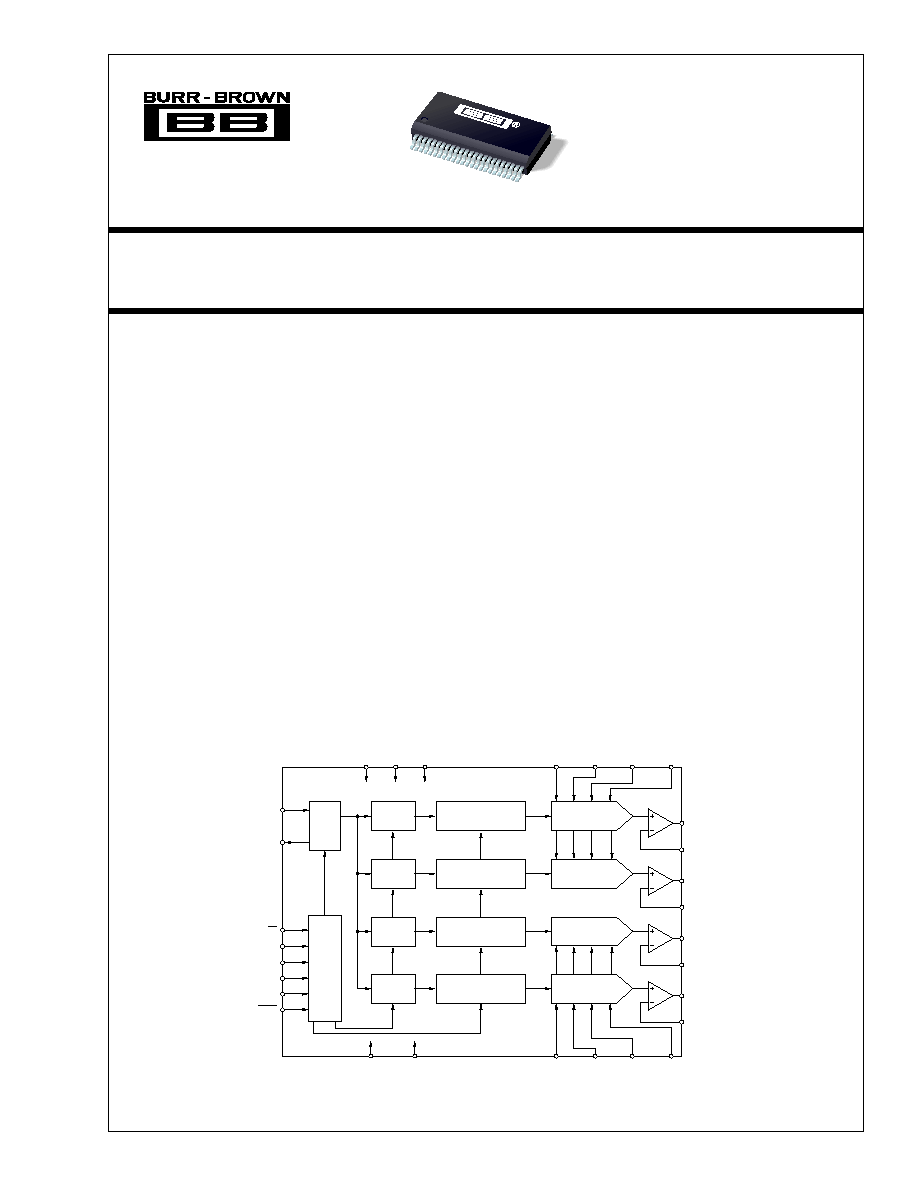
The DAC7734 is a 16-bit, quad voltage output, digital-
to-analog converter with guaranteed 16-bit monotonic
performance over the specified temperature range. It
accepts 24-bit serial input data, has double-buffered
DAC input logic (allowing simultaneous update of all
DACs), and provides a serial data output for daisy
chaining multiple DACs. Programmable asynchronous
reset clears all registers to a mid-scale code of 8000
H
or
to a zero-scale of 0000
H
. The DAC7734 can operate
from a single +15V supply or from +15V and ≠15V, and
+5V supplies.
Low power and small size per DAC make the DAC7734
ideal for automatic test equipment, DAC-per-pin pro-
grammers, data acquisition systems, and closed-loop
servo-control. The DAC7734 is available in a 48-lead
SSOP package and offers guaranteed specifications
over the ≠40
∞
C to +85
∞
C temperature range.
FEATURES
q
LOW POWER: 200mW
q
UNIPOLAR OR BIPOLAR OPERATION
q
SINGLE SUPPLY OUTPUT RANGE: +10V
q
DUAL SUPPLY OUTPUT RANGE:
±
10V
q
SETTLING TIME: 10
µ
s to 0.003%
q
16-BIT MONOTONICITY: ≠40
∞
C to +85
∞
C
q
PROGRAMMABLE RESET TO MID-SCALE
OR ZERO-SCALE
q
DOUBLE-BUFFERED DATA INPUTS
q
±
1 LSB DNL: ≠40
∞
C to +85
∞
C
APPLICATIONS
q
PROCESS CONTROL
q
ATE PIN ELECTRONICS
q
CLOSED-LOOP SERVO-CONTROL
q
MOTOR CONTROL
q
DATA ACQUISITION SYSTEMS
q
DAC-PER-PIN PROGRAMMERS
© 1999 Burr-Brown Corporation
PDS-1570A
Printed in U.S.A. December, 1999
International Airport Industrial Park ∑ Mailing Address: PO Box 11400, Tucson, AZ 85734 ∑ Street Address: 6730 S. Tucson Blvd., Tucson, AZ 85706 ∑ Tel: (520) 746-1111
Twx: 910-952-1111 ∑ Internet: http://www.burr-brown.com/ ∑ Cable: BBRCORP ∑ Telex: 066-6491 ∑ FAX: (520) 889-1510 ∑ Immediate Product Info: (800) 548-6132
For most current data sheet and other product
information, visit www.burr-brown.com
DAC A
DAC
Register A
Input
Register A
Shift
Register
DAC B
DAC
Register B
Input
Register B
DAC C
DAC
Register C
Input
Register C
DAC D
DAC
Register D
Input
Register D
V
REF
L AB
V
REF
H AB
V
REF
H
AB Sense
V
REF
L
AB Sense
V
OUT
D
V
OUT
C
V
OUT
B
V
OUT
A
V
OUT
B
Sense
V
REF
L CD V
REF
H CD
SDI
SDO
Control
Logic
CS
CLOCK
RST
RESTSEL
LDAC
LOAD
AGND
DGND
V
OUT
C
Sense
V
OUT
D
Sense
V
OUT
A
Sense
V
CC
V
SS
V
DD
DAC7734
V
REF
L
CD Sense
V
REF
H
CD Sense
DAC7734
2
Æ
DAC7734
The information provided herein is believed to be reliable; however, BURR-BROWN assumes no responsibility for inaccuracies or omissions. BURR-BROWN assumes
no responsibility for the use of this information, and all use of such information shall be entirely at the user's own risk. Prices and specifications are subject to change
without notice. No patent rights or licenses to any of the circuits described herein are implied or granted to any third party. BURR-BROWN does not authorize or warrant
any BURR-BROWN product for use in life support devices and/or systems.
DAC7734E
DAC7734EB
DAC7734EC
PARAMETER
CONDITIONS
MIN
TYP
MAX
MIN
TYP
MAX
MIN
TYP
MAX
UNITS
ACCURACY
Linearity Error (INL)
T = 25
∞
C
±
3
T
±
2
LSB
T
MIN
to T
MAX
±
4
T
±
3
LSB
Linearity Match
±
4
T
±
2
LSB
Differential Linearity Error (DNL)
T = 25
∞
C
±
3
±
2
±
1
LSB
T
MIN
to T
MAX
±
3
±
2
±
1
LSB
Monotonicity, T
MIN
to T
MAX
14
15
16
Bits
Bipolar Zero Error
T = 25
∞
C
±
0.01
±
0.025
T
T
% of FSR
Bipolar Zero Error, T
MIN
to T
MAX
±
0.05
T
T
% of FSR
Full-Scale Error
T = 25
∞
C
±
0.025
T
T
% of FSR
Full-Scale Error, T
MIN
to T
MAX
±
0.05
T
T
% of FSR
Bipolar Zero Matching
Channel-to-Channel
±
0.024
T
T
% of FSR
Matching
Full-Scale Matching
Channel-to-Channel
±
0.024
T
T
% of FSR
Matching
Power Supply Rejection Ratio (PSRR)
At Full Scale
25
T
T
ppm/V
ANALOG OUTPUT
Voltage Output
V
REF
L
V
REF
H
T
T
T
T
V
Output Current
±
5
T
T
mA
Maximum Load Capacitance
500
T
T
pF
Short-Circuit Current
±
20
T
T
mA
Short-Circuit Duration
To V
SS
, V
CC
or GND
Indefinite
T
T
REFERENCE INPUT
Ref High Input Voltage Range
V
REF
L + 1.25
+10
T
T
T
T
V
Ref Low Input Voltage Range
≠10
V
REF
H ≠ 1.25
T
T
T
T
V
Ref High Input Current
≠0.3
2.6
T
T
mA
Ref Low Input Current
≠3.2
≠0.3
T
T
mA
DYNAMIC PERFORMANCE
Settling Time
To
±
0.003%, 20V
9
11
T
T
T
T
µ
s
Output Step
Channel-to-Channel Crosstalk
See Figure 5
0.5
T
T
LSB
Digital Feedthrough
2
T
T
nV-s
Output Noise Voltage
f = 10kHz
60
T
T
nV/
Hz
DIGITAL INPUT
V
IH
0.7 ∑ V
DD
V
DD
T
T
V
V
IL
0
0.3 ∑ V
DD
T
V
I
IH
±
10
T
µ
A
I
IL
±
10
T
µ
A
DIGITAL OUTPUT
V
OH
I
OH
= ≠0.8mA
3.6
4.5
T
T
T
T
V
V
OL
I
OL
= 1.6mA
0.3
0.4
T
T
T
T
V
POWER SUPPLY
V
DD
+4.75
+5.0
+5.25
T
T
T
T
T
T
V
V
CC
+14.25
+15.0
+15.75
T
T
T
T
T
T
V
V
SS
≠14.25
≠15.0
≠15.75
T
T
T
T
T
T
V
I
DD
50
T
T
µ
A
I
CC
6
T
T
mA
I
SS
≠5
T
T
mA
Power
170
200
T
T
mW
TEMPERATURE RANGE
Specified Performance
≠40
+85
T
T
T
T
∞
C
T
Specifications same as grade to the left.
SPECIFICATIONS
(Dual Supply)
At T
A
= T
MIN
to T
MAX
, V
CC
= +15V, V
DD
= +5V, V
SS
= ≠15V, V
REF
H = +10V, and V
REF
L = ≠10V, unless otherwise noted.
3
Æ
DAC7734
DAC7734E
DAC7734EB
DAC7734EC
PARAMETER
CONDITIONS
MIN
TYP
MAX
MIN
TYP
MAX
MIN
TYP
MAX
UNITS
ACCURACY
Linearity Error
(1)
(INL)
T = 25
∞
C
±
3
T
±
2
LSB
T
MIN
to T
MAX
±
4
T
±
3
LSB
Linearity Match
±
4
T
±
2
LSB
Differential Linearity Error (DNL)
T = 25
∞
C
±
3
±
2
±
1
LSB
T
MIN
to T
MAX
±
3
±
2
±
1
LSB
Monotonicity, T
MIN
to T
MAX
14
15
16
Bits
Unipolar Zero
T = 25
∞
C
±
0.01
±
0.025
T
T
% of FSR
Unipolar Zero Error, T
MIN
to T
MAX
±
0.05
T
T
% of FSR
Full-Scale Error
T = 25
∞
C
±
0.025
T
T
% of FSR
Full-Scale Error, T
MIN
to T
MAX
±
0.05
T
T
% of FSR
Unipolar Zero Matching
Channel-to-Channel
±
0.024
T
T
% of FSR
Matching
Full-Scale Matching
Channel-to-Channel
±
0.024
T
T
% of FSR
Matching
Power Supply Rejection Ratio (PSRR)
At Full Scale
25
T
T
ppm/V
ANALOG OUTPUT
Voltage Output
V
REF
L = 0V, V
SS
= 0V
0
V
REF
H
T
T
T
T
V
R = 10k
Output Current
±
5
T
T
mA
Maximum Load Capacitance
500
T
T
pF
Short-Circuit Current
±
20
T
T
mA
Short-Circuit Duration
To V
CC
or GND
Indefinite
T
T
REFERENCE INPUT
Ref High Input Voltage Range
V
REF
L + 1.25
+10
T
T
T
T
V
Ref Low Input Voltage Range
0
V
REF
H ≠ 1.25
T
T
T
T
V
Ref High Input Current
≠0.3
1.0
T
T
mA
Ref Low Input Current
≠1.5
≠0.3
T
T
mA
DYNAMIC PERFORMANCE
Settling Time
To
±
0.003%, 10V
8
10
T
T
T
T
µ
s
Output Step
Channel-to-Channel Crosstalk
See Figure 6
0.5
T
T
LSB
Digital Feedthrough
2
T
T
nV-s
Output Noise Voltage
f = 10kHz
60
T
T
nV/
Hz
DIGITAL INPUT
V
IH
0.7 ∑ V
DD
V
DD
T
T
V
V
IL
0
0.3 ∑ V
DD
T
V
I
IH
±
10
T
µ
A
I
IL
±
10
T
µ
A
DIGITAL OUTPUT
V
OH
I
OH
= ≠0.8mA
3.6
4.5
T
T
T
T
V
V
OL
I
OL
= 1.6mA
0.3
0.4
T
T
T
T
V
POWER SUPPLY
V
DD
+4.75
+5.0
+5.25
T
T
T
T
T
T
V
V
CC
+14.25
+15.0
+15.75
T
T
T
T
T
T
V
V
SS
0
T
T
V
I
DD
50
T
T
µ
A
I
CC
3.5
T
T
mA
Power
50
70
T
T
mW
TEMPERATURE RANGE
Specified Performance
≠40
+85
T
T
T
T
∞
C
T
Specifications same as grade to the left.
NOTE: (1) If V
SS
= 0V, the specification applies at code 0021
H
and above, due to possible negative zero scale error.
SPECIFICATIONS
(Single Supply)
At T
A
= T
MIN
to T
MAX
, V
CC
= +15V, V
DD
= +5V, V
SS
= GND, V
REF
H = +10V, and V
REF
L = +50mV, unless otherwise noted.
4
Æ
DAC7734
ABSOLUTE MAXIMUM RATINGS
(1)
V
CC
to V
SS
........................................................................... ≠0.3V to +32V
V
CC
to AGND ...................................................................... ≠0.3V to +16V
V
SS
to AGND ...................................................................... +0.3V to ≠16V
AGND
to DGND ................................................................. ≠0.3V to +0.3V
V
REF
H
to AGND ..................................................................... ≠9V to +11V
V
REF
L
to AGND ...................................................................... ≠11V to +9V
V
DD
to GND ........................................................................... ≠0.3V to +6V
V
REF
H
to V
REF
L ........................................................................ ≠1V to 22V
Digital Input Voltage to GND ................................... ≠0.3V to V
DD
+ 0.3V
Digital Output Voltage to GND ................................. ≠0.3V to V
DD
+ 0.3V
Maximum Junction Temperature ................................................... +150
∞
C
Operating Temperature Range ........................................ ≠40
∞
C to +85
∞
C
Storage Temperature Range ......................................... ≠65
∞
C to +150
∞
C
Lead Temperature (soldering, 10s) ............................................... +300
∞
C
NOTE: (1) Stresses above those listed under "Absolute Maximum Ratings"
may cause permanent damage to the device. Exposure to absolute maximum
conditions for extended periods may affect device reliability.
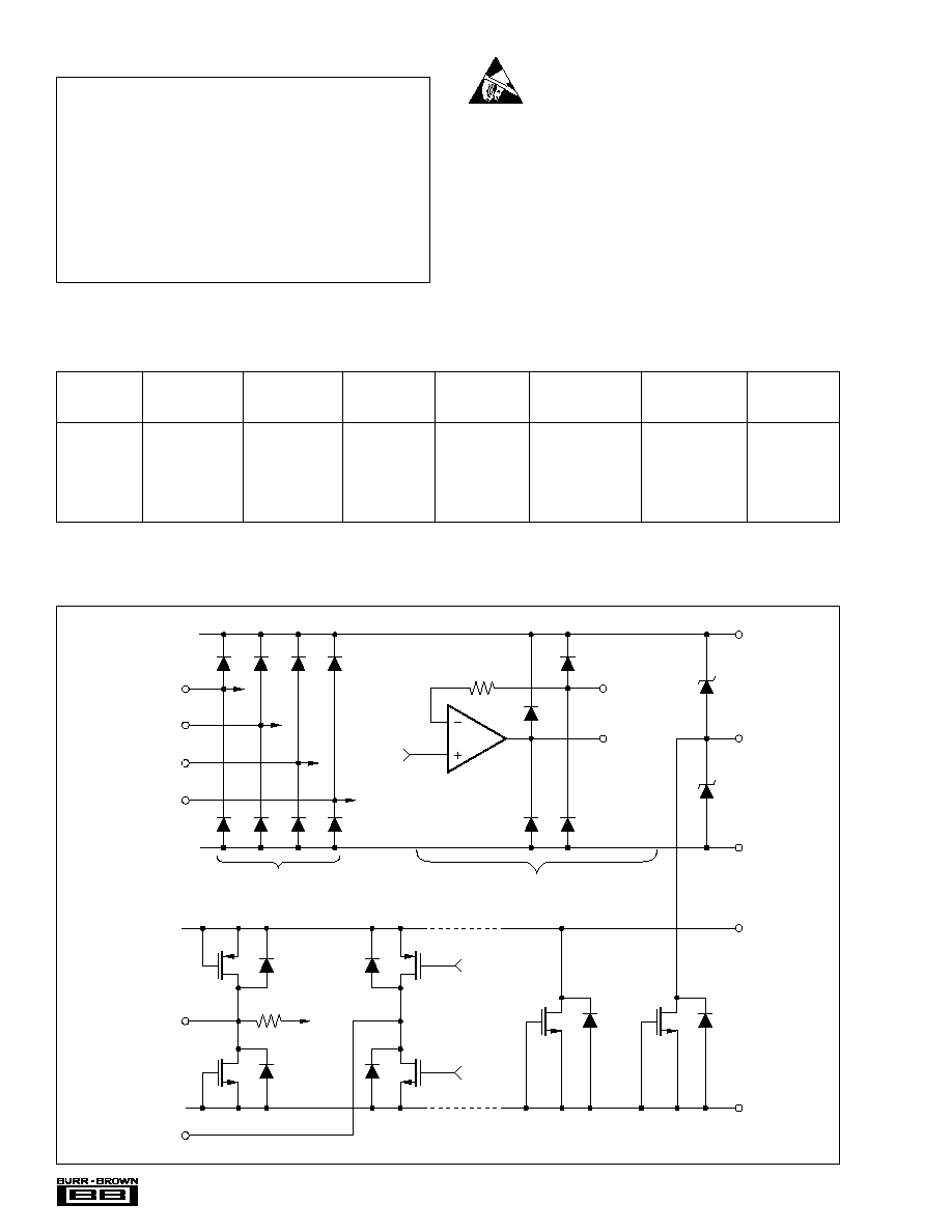
ELECTROSTATIC
DISCHARGE SENSITIVITY
This integrated circuit can be damaged by ESD. Burr-Brown
recommends that all integrated circuits be handled with
appropriate precautions. Failure to observe proper handling
and installation procedures can cause damage.
ESD damage can range from subtle performance degradation
to complete device failure. Precision integrated circuits may
be more susceptible to damage because very small parametric
changes could cause the device not to meet its published
specifications.
PACKAGE/ORDERING INFORMATION
LINEARITY
DIFFERENTIAL
PACKAGE
SPECIFICATION
ERROR
NONLINEARITY
DRAWING
TEMPERATURE
ORDERING
TRANSPORT
PRODUCT
(LSB)
(LSB)
PACKAGE
NUMBER
RANGE
NUMBER
(1)
MEDIA
DAC7734E
±
4
±
3
SSOP-48
333
≠40
∞
C to +85
∞
C
DAC7734E
Rails
"
"
"
"
"
"
DAC7734E/1K
Tape and Reel
DAC7734EB
±
4
±
2
SSOP-48
333
≠40
∞
C to +85
∞
C
DAC7734EB
Rails
"
"
"
"
"
"
DAC7734EB/1K
Tape and Reel
DAC7734EC
±
3
±
1
SSOP-48
333
≠40
∞
C to +85
∞
C
DAC7734EC
Rails
"
"
"
"
"
"
DAC7734EC/1K
Tape and Reel
NOTE: (1) Models with a slash (/) are available only in Tape and Reel in the quantities indicated (e.g., /1K indicates 1000 devices per reel). Ordering 1000 pieces
of "DAC7734E/1K" will get a single 1000-piece Tape and Reel.
ESD PROTECTION CIRCUITS
RefH
V
OUT
Sense
V
CC
V
SS
V
DD
DGND
V
CC
AGND
V
SS
V
DD
DGND
V
OUT
RefH Sense
RefL Sense
RefL
1 of 2
1 of 4
Typ of Each
Logic Input Pin
SDO
5
Æ
DAC7734
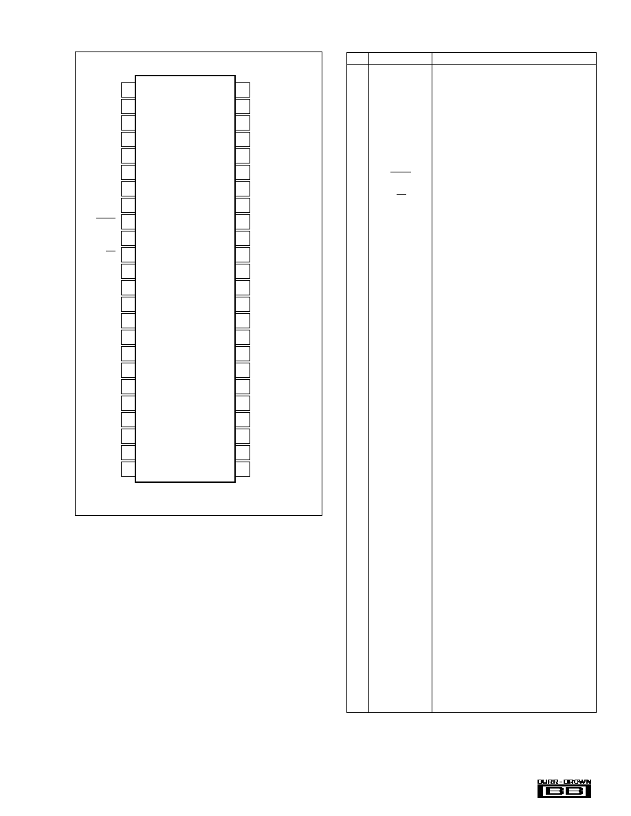
Top View
SSOP
PIN CONFIGURATION
NC
NC
SDI
DGND
CLK
DGND
LDAC
DGND
LOAD
DGND
CS
DGND
SDO
DGND
RSTSEL
DGND
RST
DGND
NC
NC
DGND
DGND
V
DD
V
DD
V
OUT
A Sense
V
OUT
A
AGND
V
SS
V
REF
L AB Sense
V
REF
L AB
V
REF
H AB
V
REF
H AB Sense
V
OUT
B Sense
V
OUT
B
V
OUT
C Sense
V
OUT
C
V
REF
H CD Sense
V
REF
H CD
V
REF
L CD
V
REF
L CD Sense
V
OUT
D Sense
V
OUT
D
V
SS
V
SS
AGND
AGND
V
CC
V
CC
1
2
3
4
5
6
7
8
9
10
11
12
13
14
15
16
17
18
19
20
21
22
23
24
48
47
46
45
44
43
42
41
40
39
38
37
36
35
34
33
32
31
30
29
28
27
26
25
DAC7734
PIN
NAME
DESCRIPTION
1
NC
No Connection
2
NC
No Connection
3
SDI
Serial Data Input
4
DGND
Digital Ground
5
CLK
Data Clock Input
6
DGND
Digital Ground
7
LDAC
DAC Register Load Control, Rising Edge
Triggered
8
DGND
Digital Ground
9
LOAD
DAC Input Register Load Control, Active Low
10
DGND
Digital Ground
11
CS
Chip Select, Active Low
12
DGND
Digital Ground
13
SDO
Serial Data Output
14
DGND
Digital Ground
15
RSTSEL
Reset Select. Determines the action of RST. If
HIGH, a RST common will set the DAC registers
to mid-scale (8000H). If LOW, a RST command
will set the DAC registers to zero (0000H).
16
DGND
Digital Ground
17
RST
Reset, Rising Edge Triggered. Depending on the
state of RSTSEL, the DAC registers are set to
either mid-scale or zero.
18
DGND
Digital Ground
19
NC
No Connection
20
NC
No Connection
21
DGND
Digital Ground
22
DGND
Digital Ground
23
V
DD
Digital +5V Power Supply
24
V
DD
Digital +5V Power Supply
25
V
CC
Analog +15V Power Supply
26
V
CC
Analog +15V Power Supply
27
AGND
Analog Ground
28
AGND
Analog Ground
29
V
SS
Analog ≠15V Power Supply or 0V Single Supply
30
V
SS
Analog ≠15V Power Supply or 0V Single Supply
31
V
OUT
D
DAC D Output Voltage
32
V
OUT
D Sense
DAC D's Output Amplifier Inverting Input. Used
to close feedback loop at load.
33
V
REF
L CD Sense
DAC C and D Reference Low Sense Input
34
V
REF
L CD
DAC C and D Reference Low Input
35
V
REF
H CD
DAC C and D Reference High Input
36
V
REF
H CD Sense
DAC C and D Reference High Sense Input
37
V
OUT
C
DAC C Output Voltage
38
V
OUT
C Sense
DAC C's Output Amplifier Inverting Input. Used
to close the feedback loop at the load.
39
V
OUT
B
DAC B Output Voltage
40
V
OUT
B Sense
DAC B's Output Amplifier Inverting Input. Used
to close the feedback loop at the load.
41
V
REF
H AB Sense
DAC A and B Reference High Sense Input
42
V
REF
H AB
DAC A and B Reference High Input
43
V
OUT
L AB
DAC A and B Reference Low Input
44
V
REF
L AB Sense
DAC A and B Reference Low Sense Input
45
V
SS
Analog ≠15V Power Supply or 0V Single Supply
46
AGND
Analog Ground
47
V
OUT
A
DAC A Output Voltage
48
V
OUT
A Sense
DAC A's Output Amplifier Inverting Input. Used
to close the feedback loop at the load.
PIN DESCRIPTIONS

6
Æ
DAC7734
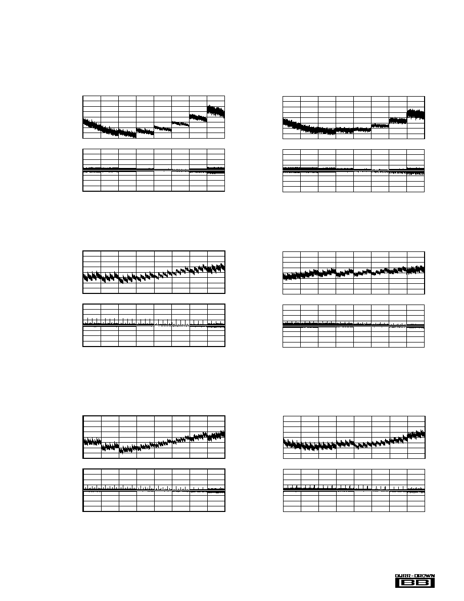
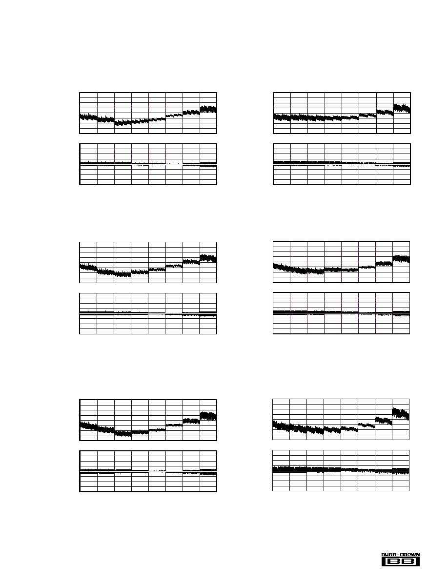
TYPICAL PERFORMANCE CURVES: V
SS
= 0V
At T
A
= +25
∞
C, V
DD
= +5V, V
CC
= +15V, V
SS
= 0, V
REF
H
= +10V, and V
REF
L
= 0V, representative unit, unless otherwise specified.
+25
∞
C
+85
∞
C
2.0
1.5
1.0
0.5
0
≠0.5
≠1.0
≠1.5
≠2.0
2.0
1.5
1.0
0.5
0
≠0.5
≠1.0
≠1.5
≠2.0
LE (LSB)
DLE (LSB)
LINEARITY ERROR AND
DIFFERENTIAL LINEARITY ERROR vs CODE
(DAC A, +25
∞
C)
0000
H
2000
H
4000
H
6000
H
8000
H
Digital Input Code
A000
H
C000
H
E000
H
FFFF
H
2.0
1.5
1.0
0.5
0
≠0.5
≠1.0
≠1.5
≠2.0
2.0
1.5
1.0
0.5
0
≠0.5
≠1.0
≠1.5
≠2.0
LE (LSB)
DLE (LSB)
LINEARITY ERROR AND
DIFFERENTIAL LINEARITY ERROR vs CODE
(DAC A, +85
∞
C)
0000
H
2000
H
4000
H
6000
H
8000
H
Digital Input Code
A000
H
C000
H
E000
H
FFFF
H
2.0
1.5
1.0
0.5
0
≠0.5
≠1.0
≠1.5
≠2.0
2.0
1.5
1.0
0.5
0
≠0.5
≠1.0
≠1.5
≠2.0
LE (LSB)
DLE (LSB)
LINEARITY ERROR AND
DIFFERENTIAL LINEARITY ERROR vs CODE
(DAC D, +25
∞
C)
0000
H
2000
H
4000
H
6000
H
8000
H
Digital Input Code
A000
H
C000
H
E000
H
FFFF
H
2.0
1.5
1.0
0.5
0
≠0.5
≠1.0
≠1.5
≠2.0
2.0
1.5
1.0
0.5
0
≠0.5
≠1.0
≠1.5
≠2.0
LE (LSB)
DLE (LSB)
LINEARITY ERROR AND
DIFFERENTIAL LINEARITY ERROR vs CODE
(DAC B, +25
∞
C)
0000
H
2000
H
4000
H
6000
H
8000
H
Digital Input Code
A000
H
C000
H
E000
H
FFFF
H
2.0
1.5
1.0
0.5
0
≠0.5
≠1.0
≠1.5
≠2.0
2.0
1.5
1.0
0.5
0
≠0.5
≠1.0
≠1.5
≠2.0
LE (LSB)
DLE (LSB)
LINEARITY ERROR AND
DIFFERENTIAL LINEARITY ERROR vs CODE
(DAC B, +85
∞
C)
0000
H
2000
H
4000
H
6000
H
8000
H
Digital Input Code
A000
H
C000
H
E000
H
FFFF
H
2.0
1.5
1.0
0.5
0
≠0.5
≠1.0
≠1.5
≠2.0
2.0
1.5
1.0
0.5
0
≠0.5
≠1.0
≠1.5
≠2.0
LE (LSB)
DLE (LSB)
LINEARITY ERROR AND
DIFFERENTIAL LINEARITY ERROR vs CODE
(DAC C, +25
∞
C)
0000
H
2000
H
4000
H
6000
H
8000
H
Digital Input Code
A000
H
C000
H
E000
H
FFFF
H
7
Æ
DAC7734
2.0
1.5
1.0
0.5
0
≠0.5
≠1.0
≠1.5
≠2.0
2.0
1.5
1.0
0.5
0
≠0.5
≠1.0
≠1.5
≠2.0
LE (LSB)
DLE (LSB)
LINEARITY ERROR AND
DIFFERENTIAL LINEARITY ERROR vs CODE
(DAC A, ≠40
∞
C)
0000
H
2000
H
4000
H
6000
H
8000
H
Digital Input Code
A000
H
C000
H
E000
H
FFFF
H
2.0
1.5
1.0
0.5
0
≠0.5
≠1.0
≠1.5
≠2.0
2.0
1.5
1.0
0.5
0
≠0.5
≠1.0
≠1.5
≠2.0
LE (LSB)
DLE (LSB)
LINEARITY ERROR AND
DIFFERENTIAL LINEARITY ERROR vs CODE
(DAC D, ≠40
∞
C)
0000
H
2000
H
4000
H
6000
H
8000
H
Digital Input Code
A000
H
C000
H
E000
H
FFFF
H
2.0
1.5
1.0
0.5
0
≠0.5
≠1.0
≠1.5
≠2.0
2.0
1.5
1.0
0.5
0
≠0.5
≠1.0
≠1.5
≠2.0
LE (LSB)
DLE (LSB)
LINEARITY ERROR AND
DIFFERENTIAL LINEARITY ERROR vs CODE
(DAC D, +85
∞
C)
0000
H
2000
H
4000
H
6000
H
8000
H
Digital Input Code
A000
H
C000
H
E000
H
FFFF
H
TYPICAL PERFORMANCE CURVES: V
SS
= 0V
(Cont.)
At T
A
= +25
∞
C, V
DD
= +5V, V
CC
= +15V, V
SS
= 0, V
REF
H
= +10V, and V
REF
L
= 0V, representative unit, unless otherwise specified.
+85
∞
C
(cont.)
≠40
∞
C
2.0
1.5
1.0
0.5
0
≠0.5
≠1.0
≠1.5
≠2.0
2.0
1.5
1.0
0.5
0
≠0.5
≠1.0
≠1.5
≠2.0
LE (LSB)
DLE (LSB)
LINEARITY ERROR AND
DIFFERENTIAL LINEARITY ERROR vs CODE
(DAC B, ≠40
∞
C)
0000
H
2000
H
4000
H
6000
H
8000
H
Digital Input Code
A000
H
C000
H
E000
H
FFFF
H
2.0
1.5
1.0
0.5
0
≠0.5
≠1.0
≠1.5
≠2.0
2.0
1.5
1.0
0.5
0
≠0.5
≠1.0
≠1.5
≠2.0
LE (LSB)
DLE (LSB)
LINEARITY ERROR AND
DIFFERENTIAL LINEARITY ERROR vs CODE
(DAC C, +85
∞
C)
0000
H
2000
H
4000
H
6000
H
8000
H
Digital Input Code
A000
H
C000
H
E000
H
FFFF
H
2.0
1.5
1.0
0.5
0
≠0.5
≠1.0
≠1.5
≠2.0
2.0
1.5
1.0
0.5
0
≠0.5
≠1.0
≠1.5
≠2.0
LE (LSB)
DLE (LSB)
LINEARITY ERROR AND
DIFFERENTIAL LINEARITY ERROR vs CODE
(DAC C, ≠40
∞
C)
0000
H
2000
H
4000
H
6000
H
8000
H
Digital Input Code
A000
H
C000
H
E000
H
FFFF
H
8
Æ
DAC7734
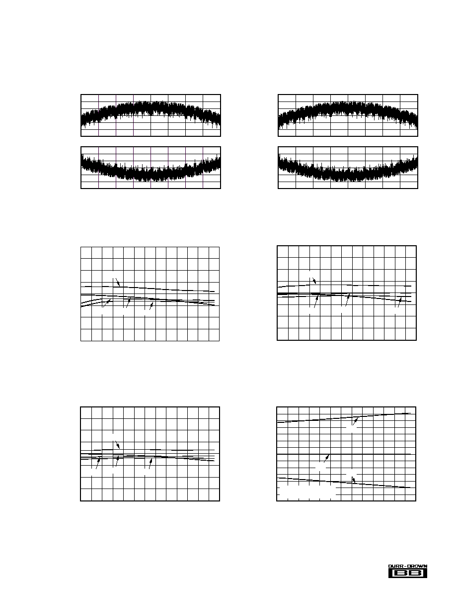
TYPICAL PERFORMANCE CURVES: V
SS
= 0V
(Cont.)
At T
A
= +25
∞
C, V
DD
= +5V, V
CC
= +15V, V
SS
= 0, V
REF
H
= +10V, and V
REF
L
= 0V, representative unit, unless otherwise specified.
1.0
0.8
0.6
0.4
0.2
0
≠0.2
≠0.4
V
REF
(Current (mA)
REFERENCE CURRENT vs CODE
All DACs Sent to Indicated Code
(DAC A and B)
V
REFH
V
REFL
0000
H
2000
H
4000
H
6000
H
8000
H
Digital Input Code
A000
H
C000
H
E000
H
FFFF
H
0
≠0.2
≠0.4
≠0.6
≠0.8
≠1.0
≠1.2
≠1.4
V
REF
(Current (mA)
1.0
0.8
0.6
0.4
0.2
0
≠0.2
≠0.4
V
REF
(Current (mA)
REFERENCE CURRENT vs CODE
All DACs Sent to Indicated Code
(DAC C and D)
V
REFH
V
REFL
0000
H
2000
H
4000
H
6000
H
8000
H
Digital Input Code
A000
H
C000
H
E000
H
FFFF
H
0
≠0.2
≠0.4
≠0.6
≠0.8
≠1.0
≠1.2
≠1.4
V
REF
(Current (mA)
2
1.5
1
0.5
0
≠0.5
≠1
≠1.5
≠2
Temperature (
∞
C)
≠40 ≠30
≠10
0
≠20
10
20
40
50
30
70
80
90
60
ZERO-SCALE ERROR vs TEMPERATURE
Negative Full-Scale Error (mV)
Code (0040
H
)
Code (0000
H
)
DAC D
DAC A
DAC C
DAC B
2
1.5
1
0.5
0
≠0.5
≠1
≠1.5
≠2
Temperature (
∞
C)
≠40 ≠30
≠10
0
≠20
10
20
40
50
30
70
80
90
60
POSITIVE FULL-SCALE ERROR
vs TEMPERATURE
Positive Full-Scale Error (mV)
DAC A
DAC D
DAC B
DAC C
Code (FFFF
H
)
4.0
3.5
3.0
2.5
2.0
1.5
1.0
0.5
0
≠0.5
Temperature (
∞
C)
≠40 ≠30
≠10
0
≠20
10
20
40
50
30
70
80
90
60
POWER SUPPLY CURRENT vs TEMPERATURE
Quiescent Current (mA)
I
CC
I
DD
Data = FFFF
H
(all DACs)
No Load
4.0
3.5
3.0
2.5
2.0
1.5
1.0
0.5
0
≠0.5
Digital Input Code
0
2000
H
4000
H
6000
H
8000
H
A000
H
C000
H
E000
H
FFFF
H
POSITIVE SUPPLY CURRENT
vs DIGITAL INPUT CODE
I
CC
(mA)
No Load
I
CC
I
DD

9
Æ
DAC7734
TYPICAL PERFORMANCE CURVES: V
SS
= 0V
(Cont.)
At T
A
= +25
∞
C, V
DD
= +5V, V
CC
= +15V, V
SS
= 0, V
REF
H
= +10V, and V
REF
L
= 0V, representative unit, unless otherwise specified.
+5V
LDAC
0
Time (2
µ
s/div)
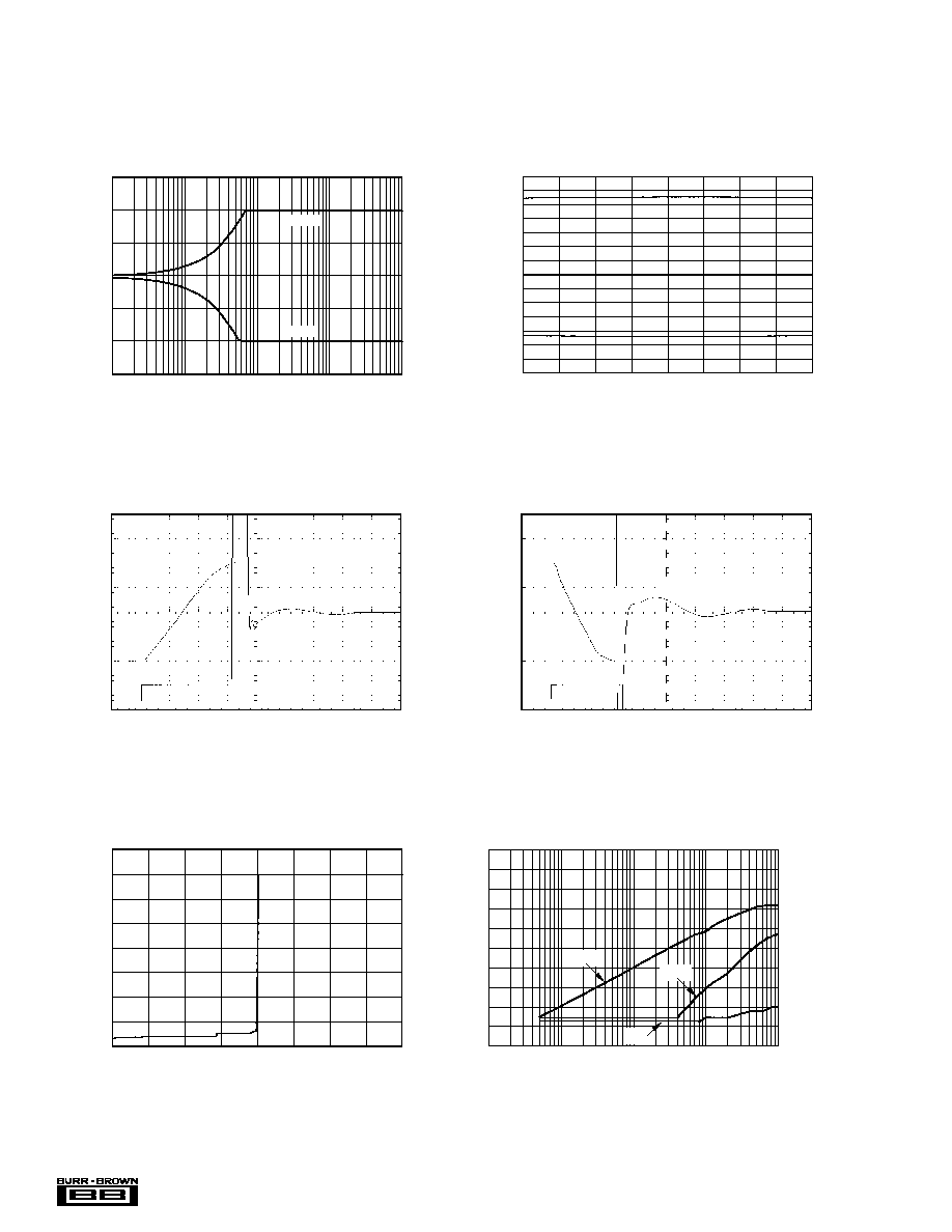
OUTPUT VOLTAGE vs SETTLING TIME
(0V to +10V)
Output Voltage
+5V
LDAC
0
Time (2
µ
s/div)
OUTPUT VOLTAGE vs SETTLING TIME
(+10V to 0V)
Output Voltage
+5V
LDAC
0
Time (1
µ
s/div)
OUTPUT VOLTAGE
MIDSCALE GLITCH PERFORMANCE
Output Voltage (200mV/div)
+5V
LDAC
0
Time (1
µ
s/div)
Output Voltage (200mV/div)
OUTPUT VOLTAGE
MIDSCALE GLITCH PERFORMANCE
BROADBAND NOISE
Time (100
µ
s/div)
Noise Voltage (20
µ
V/div)
BW = 10kHz
Code = 8000
H
120
100
80
60
40
20
0
Frequency (Hz)
100
1k
10k
100k
1M
OUTPUT NOISE VOLTAGE vs FREQUENCY
Noise (nV/
Hz)
Large-Signal Settling Time: 5V/div
Small-Signal Settling Time:
3LSB/div
Large-Signal Settling Time: 5V/div
Small-Signal Settling Time:
3LSB/div
7FFF
H
to 8000
H
8000
H
to 7FFF
H
10
Æ
DAC7734
TYPICAL PERFORMANCE CURVES: V
SS
= 0V
(Cont.)
At T
A
= +25
∞
C, V
DD
= +5V, V
CC
= +15V, V
SS
= 0, V
REF
H
= +10V, and V
REF
L
= 0V, representative unit, unless otherwise specified.
16
14
12
10
8
6
4
2
0
R
LOAD
(k
)
0.01
0.1
1
10
100
OUTPUT VOLTAGE vs R
LOAD
V
OUT
(V)
Source
Sink
30
25
20
15
10
5
0
≠5
≠10
≠15
≠20
≠25
≠30
Input Code
0000
H
2000
H
4000
H
6000
H
8000
H
A000
H
C000
H
E000
H
FFFF
H
SINGLE-SUPPLY CURRENT LIMIT vs INPUT CODE
I
OUT
(mA)
Short to Ground
Short to V
CC
0
≠10
≠20
≠30
≠40
≠50
≠60
≠70
≠80
≠90
Frequency (Hz)
100
1k
10k
100k
1M
POWER SUPPLY REJECTION RATIO vs FREQUENCY
PSRR (dB)
+15V
+5V
+5V
CLK
0V
Time (50ns/div)
CLOCK FEEDTHROUGH
Output Voltage (5mV/div)
11
Æ
DAC7734
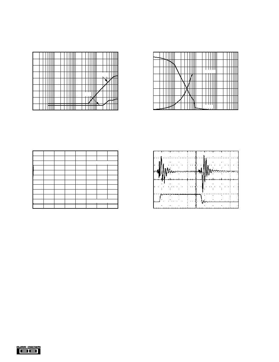
TYPICAL PERFORMANCE CURVES: V
SS
= ≠15V
At T
A
= +25
∞
C, V
DD
= +5V, V
CC
= +15V, V
SS
= ≠15V, V
REF
H
= +10V, and V
REF
L
= ≠10V, representative unit, unless otherwise specified.
+85
∞
C
+25
∞
C
2.0
1.5
1.0
0.5
0
≠0.5
≠1.0
≠1.5
≠2.0
2.0
1.5
1.0
0.5
0
≠0.5
≠1.0
≠1.5
≠2.0
LE (LSB)
DLE (LSB)
LINEARITY ERROR AND
DIFFERENTIAL LINEARITY ERROR vs CODE
(DAC A, +25
∞
C)
0000
H
2000
H
4000
H
6000
H
8000
H
Digital Input Code
A000
H
C000
H
E000
H
FFFF
H
2.0
1.5
1.0
0.5
0
≠0.5
≠1.0
≠1.5
≠2.0
2.0
1.5
1.0
0.5
0
≠0.5
≠1.0
≠1.5
≠2.0
LE (LSB)
DLE (LSB)
LINEARITY ERROR AND
DIFFERENTIAL LINEARITY ERROR vs CODE
(DAC A, +85
∞
C)
0000
H
2000
H
4000
H
6000
H
8000
H
Digital Input Code
A000
H
C000
H
E000
H
FFFF
H
2.0
1.5
1.0
0.5
0
≠0.5
≠1.0
≠1.5
≠2.0
2.0
1.5
1.0
0.5
0
≠0.5
≠1.0
≠1.5
≠2.0
LE (LSB)
DLE (LSB)
LINEARITY ERROR AND
DIFFERENTIAL LINEARITY ERROR vs CODE
(DAC B, +25
∞
C)
0000
H
2000
H
4000
H
6000
H
8000
H
Digital Input Code
A000
H
C000
H
E000
H
FFFF
H
2.0
1.5
1.0
0.5
0
≠0.5
≠1.0
≠1.5
≠2.0
2.0
1.5
1.0
0.5
0
≠0.5
≠1.0
≠1.5
≠2.0
LE (LSB)
DLE (LSB)
LINEARITY ERROR AND
DIFFERENTIAL LINEARITY ERROR vs CODE
(DAC B, +85
∞
C)
0000
H
2000
H
4000
H
6000
H
8000
H
Digital Input Code
A000
H
C000
H
E000
H
FFFF
H
2.0
1.5
1.0
0.5
0
≠0.5
≠1.0
≠1.5
≠2.0
2.0
1.5
1.0
0.5
0
≠0.5
≠1.0
≠1.5
≠2.0
LE (LSB)
DLE (LSB)
LINEARITY ERROR AND
DIFFERENTIAL LINEARITY ERROR vs CODE
(DAC C, +25
∞
C)
0000
H
2000
H
4000
H
6000
H
8000
H
Digital Input Code
A000
H
C000
H
E000
H
FFFF
H
2.0
1.5
1.0
0.5
0
≠0.5
≠1.0
≠1.5
≠2.0
LE (LSB)
LINEARITY ERROR AND
DIFFERENTIAL LINEARITY ERROR vs CODE
(DAC D, +25
∞
C)
0000
H
2000
H
4000
H
6000
H
8000
H
Digital Input Code
A000
H
C000
H
E000
H
FFFF
H
2.0
1.5
1.0
0.5
0
≠0.5
≠1.0
≠1.5
≠2.0
DLE (LSB)

12
Æ
DAC7734
TYPICAL PERFORMANCE CURVES: V
SS
= ≠15V
(Cont.)
At T
A
= +25
∞
C, V
DD
= +5V, V
CC
= +15V, V
SS
= ≠15V, V
REF
H
= +10V, and V
REF
L
= ≠10V, representative unit, unless otherwise specified.
+85
∞
C
(cont.)
≠40
∞
C
2.0
1.5
1.0
0.5
0
≠0.5
≠1.0
≠1.5
≠2.0
2.0
1.5
1.0
0.5
0
≠0.5
≠1.0
≠1.5
≠2.0
LE (LSB)
DLE (LSB)
LINEARITY ERROR AND
DIFFERENTIAL LINEARITY ERROR vs CODE
(DAC A, ≠40
∞
C)
0000
H
2000
H
4000
H
6000
H
8000
H
Digital Input Code
A000
H
C000
H
E000
H
FFFF
H
2.0
1.5
1.0
0.5
0
≠0.5
≠1.0
≠1.5
≠2.0
2.0
1.5
1.0
0.5
0
≠0.5
≠1.0
≠1.5
≠2.0
LE (LSB)
DLE (LSB)
LINEARITY ERROR AND
DIFFERENTIAL LINEARITY ERROR vs CODE
(DAC B, ≠40
∞
C)
0000
H
2000
H
4000
H
6000
H
8000
H
Digital Input Code
A000
H
C000
H
E000
H
FFFF
H
2.0
1.5
1.0
0.5
0
≠0.5
≠1.0
≠1.5
≠2.0
2.0
1.5
1.0
0.5
0
≠0.5
≠1.0
≠1.5
≠2.0
LE (LSB)
DLE (LSB)
LINEARITY ERROR AND
DIFFERENTIAL LINEARITY ERROR vs CODE
(DAC C, ≠40
∞
C)
0000
H
2000
H
4000
H
6000
H
8000
H
Digital Input Code
A000
H
C000
H
E000
H
FFFF
H
2.0
1.5
1.0
0.5
0
≠0.5
≠1.0
≠1.5
≠2.0
2.0
1.5
1.0
0.5
0
≠0.5
≠1.0
≠1.5
≠2.0
LE (LSB)
DLE (LSB)
LINEARITY ERROR AND
DIFFERENTIAL LINEARITY ERROR vs CODE
(DAC C, +85
∞
C)
0000
H
2000
H
4000
H
6000
H
8000
H
Digital Input Code
A000
H
C000
H
E000
H
FFFF
H
2.0
1.5
1.0
0.5
0
≠0.5
≠1.0
≠1.5
≠2.0
LE (LSB)
LINEARITY ERROR AND
DIFFERENTIAL LINEARITY ERROR vs CODE
(DAC D, +85
∞
C)
0000
H
2000
H
4000
H
6000
H
8000
H
Digital Input Code
A000
H
C000
H
E000
H
FFFF
H
2.0
1.5
1.0
0.5
0
≠0.5
≠1.0
≠1.5
≠2.0
DLE (LSB)
2.0
1.5
1.0
0.5
0
≠0.5
≠1.0
≠1.5
≠2.0
LE (LSB)
LINEARITY ERROR AND
DIFFERENTIAL LINEARITY ERROR vs CODE
(DAC D, ≠40
∞
C)
0000
H
2000
H
4000
H
6000
H
8000
H
Digital Input Code
A000
H
C000
H
E000
H
FFFF
H
2.0
1.5
1.0
0.5
0
≠0.5
≠1.0
≠1.5
≠2.0
DLE (LSB)
13
Æ
DAC7734
TYPICAL PERFORMANCE CURVES: V
SS
= ≠15V
(Cont.)
At T
A
= +25
∞
C, V
DD
= +5V, V
CC
= +15V, V
SS
= ≠15V, V
REF
H
= +10V, and V
REF
L
= ≠10V, representative unit, unless otherwise specified.
2.5
2.0
1.5
1.0
0.5
0
≠0.5
V
REF
(Current (mA)
REFERENCE CURRENT vs CODE
All DACs Sent to Indicated Code
(DAC A and B)
V
REFH
V
REFL
0000
H
2000
H
4000
H
6000
H
8000
H
Digital Input Code
A000
H
C000
H
E000
H
FFFF
H
0.0
≠0.5
≠1.0
≠1.5
≠2.0
≠2.5
≠3.0
V
REF
(Current (mA)
2.5
2.0
1.5
1.0
0.5
0
≠0.5
V
REF
(Current (mA)
REFERENCE CURRENT vs CODE
All DACs Sent to Indicated Code
(DAC C and D)
V
REFH
VREFL
0000
H
2000
H
4000
H
6000
H
8000
H
Digital Input Code
A000
H
C000
H
E000
H
FFFF
H
0.0
≠0.5
≠1.0
≠1.5
≠2.0
≠2.5
≠3.0
V
REF
(Current (mA)
2
1.5
1
0.5
0
≠0.5
≠1
≠1.5
≠2
Temperature (
∞
C)
≠40 ≠30 ≠20 ≠10
0
10
20
30
40
50
60
70
80
90
BIPOLAR ZERO SCALE ERROR vs TEMPERATURE
(Code 8000
H
)
Bipolar Zero Scale Error (mV)
DAC A
DAC D
DAC C
DAC B
2
1.5
1.0
0.5
0
≠0.5
≠1.0
≠1.5
≠2.0
Temperature (
∞
C)
≠40
≠10
0
≠30 ≠20
90
10
20
30
40
50 60
70
80
POSITIVE FULL-SCALE ERROR vs TEMPERATURE
(Code FFFF
H
)
Positive Full-Scale Error (mV)
DAC A
DAC B
DAC D
DAC C
2
1.5
1.0
0.5
0
≠0.5
≠1.0
≠1.5
≠2.0
Temperature (
∞
C)
≠40
≠10
0
≠30 ≠20
90
10
20
30
40
50 60
70
80
NEGATIVE FULL-SCALE ERROR vs TEMPERATURE
(Code 0000
H
)
Negative Full-Scale Error (mV)
DAC A
DAC D
DAC B
DAC C
7
6
5
4
3
2
1
0
≠1
≠2
≠3
≠4
≠5
≠6
≠7
Temperature (
∞
C)
≠40
≠10
0
≠30 ≠20
90
10
20
30
40
50 60
70
80
POWER SUPPLY CURRENT vs TEMPERTURE
Quiescent Current (mA)
I
SS
I
CC
I
DD
Data = FFFF
H
(all DACs)
No Load
14
Æ
DAC7734
Time (2
µ
s/div)
OUTPUT VOLTAGE vs SETTLING TIME
(≠10V to +10V)
Output Voltage
+5V
LDAC
0
TYPICAL PERFORMANCE CURVES: V
SS
= ≠15V
(Cont.)
At T
A
= +25
∞
C, V
DD
= +5V, V
CC
= +15V, V
SS
= ≠15V, V
REF
H
= +10V, and V
REF
L
= ≠10V, representative unit, unless otherwise specified.
15
10
5
0
≠5
≠10
≠15
R
LOAD
(k
)
0.01
0.1
1
10
100
OUTPUT VOLTAGE vs R
LOAD
V
OUT
(V)
Sink
Source
7
6
5
4
3
2
1
0
≠1
≠2
≠3
≠4
≠5
≠6
≠7
SUPPLY CURRENT vs CODE
(mA)
Digital Input Code
0000
H
2000
H
4000
H
6000
H
8000
H
A000
H
C000
H
E000
H
FFFF
H
I
CC
I
DD
I
SS
Time (2
µ
s/div)
OUTPUT VOLTAGE vs SETTLING TIME
(+10V to ≠10V)
Output Voltage
+5V
LDAC
0
20
15
10
5
0
≠5
≠10
≠15
≠20
Digital Input Code
0000
H
2000
H
4000
H
6000
H
8000
H
A000
H
C000
H
E000
H
FFFF
H
DUAL-SUPPLY CURRENT LIMIT vs INPUT CODE
(Short-to-Ground)
I
OUT
(mA)
Large-Signal Settling Time: 5V/div
Small-Signal Settling Time: 3LSB/div
Large-Signal Settling Time: 5V/div
Small-Signal Settling Time: 3LSB/div
0
≠10
≠20
≠30
≠40
≠50
≠60
≠70
≠80
≠90
≠100
Frequency (Hz)
100
1k
10k
100k
1M
POWER SUPPLY REJECTION RATIO vs FREQUENCY
PSRR (dB)
≠15V
+15V
+5V
15
Æ
DAC7734
Time (1
µ
s/div)
OUTPUT VOLTAGE
MID-SCALE GLITCH PERFORMANCE
Output Voltage (200mV/div)
+5V
LDAC
0
TYPICAL PERFORMANCE CURVES: V
SS
= ≠15V
(Cont.)
At T
A
= +25
∞
C, V
DD
= +5V, V
CC
= +15V, V
SS
= ≠15V, V
REF
H
= +10V, and V
REF
L
= ≠10V, representative unit, unless otherwise specified.
Time (1
µ
s/div)
OUTPUT VOLTAGE
MID-SCALE GLITCH PERFORMANCE
Output Voltage (200mV/div)
+5V
LDAC
0
7FFF
H
to 8000
H
8000
H
to 7FFF
H

16
Æ
DAC7734
THEORY OF OPERATION
The DAC7734 is a quad voltage output, 16-bit Digital-to-
Analog Converter (DAC). The architecture is an R-2R
ladder configuration with the three MSB's segmented, fol-
lowed by an operational amplifier that serves as a buffer.
Each DAC has its own R-2R ladder network, segmented
MSBs, and output op amp, as shown in Figure 1. The
minimum voltage output (zero-scale) and maximum voltage
output (full-scale) are set by the external voltage references
V
REF
L and V
REF
H.
The digital input is a 24-bit serial word that contains a 2-bit
address code for selecting one of four DACs, a quick load
bit, five unused bits and the 16-bit DAC code (MSB first).
The converters can be powered from either a single +15V
supply or a dual
±
15V supply and a +5V logic supply. The
device offers a reset function which immediately sets all
DAC output voltages and DAC registers to mid-scale code
8000
H
or to zero-scale, code 0000
H
. See Figures 2 and 3 for
the basic operation of the DAC7734.
FIGURE 1. DAC7734 Architecture.
FIGURE 2. Basic Single-Supply Operation of the DAC7734.
R
2R
2R
2R
2R
2R
2R
2R
2R
2R
V
REF
H
V
OUT
V
OUT
Sense
V
REF
H Sense
V
REF
L
V
REF
L Sense
R
F
NC
NC
SDI
DGND
CLK
DGND
LDAC
DGND
LOAD
DGND
CS
DGND
SDO
DGND
RSTSEL
DGND
RST
DGND
NC
NC
DGND
DGND
V
DD
V
DD
V
OUT
A Sense
V
OUT
A
AGND
V
SS
V
REF
L AB Sense
V
REF
L AB
V
REF
H AB
V
REF
H AB Sense
V
OUT
B Sense
V
OUT
B
V
OUT
C Sense
V
OUT
C
V
REF
H CD Sense
V
REF
H CD
V
REF
L CD
V
REF
L CD Sense
V
OUT
D Sense
V
OUT
D
V
SS
V
SS
AGND
AGND
V
CC
V
CC
1
2
3
4
5
6
7
8
9
10
11
12
13
14
15
16
17
18
19
20
21
22
23
24
48
47
46
45
44
43
42
41
40
39
38
37
36
35
34
33
32
31
30
29
28
27
26
25
DAC7734
Reset DAC Registers
Chips Select
Serial Data Out
Serial Data In
Clock
Load DAC Registers
Load
NC = No Connection
0V to +10V
0V to +10V
0V to +10V
0V to +10V
+10.000V
+10.000V
+15V
0.1
µ
F
1
µ
F
+
0.1
µ
F
1
µ
F
+5V
+

17
Æ
DAC7734
FIGURE 3. Basic Dual-Supply Operation of the DAC7734.
ANALOG OUTPUTS
When V
SS
= ≠15V (dual supply operation), the output
amplifier can swing to within 4V of the supply rails, guar-
anteed over the ≠40
∞
C to +85
∞
C temperature range. When
V
SS
= 0V (single-supply operation), and with R
LOAD
also
connected to ground, the output can swing to ground. Care
must also be taken when measuring the zero-scale error
when V
SS
= 0V. Since the output voltage cannot swing
below ground, the output voltage may not change for the
first few digital input codes (0000
H
, 0001
H
, 0002
H
, etc.) if
the output amplifier has a negative offset. At the negative
limit of ≠5mV, the first specified output starts at code 0021
H
.
Due to the high accuracy of these D/A converters, system
design problems such as grounding and contact resistance
become very important. A 16-bit converter with a 10V full-
scale range has a 1LSB value of 152
µ
V. With a load current
of 1mA, series wiring and connector resistance of only
150m
(R
W2
) will cause a voltage drop of 150
µ
V, as shown
in Figure 4. To understand what this means in terms of a
system layout, the resistivity of a typical 1 ounce copper-
clad printed circuit board is 1/2 m
per square. For a 1mA
load, a 20 milli-inch wide printed circuit conductor 6 inches
long will result in a voltage drop of 150
µ
V.
The DAC7734 offers a force and sense output configuration
for the high open-loop gain output amplifier. This feature
allows the loop around the output amplifier to be closed at
the load (as shown in Figure 4), thus ensuring an accurate
output voltage.
FIGURE 4. Analog Output Closed-Loop Configuration
(1/2 DAC7734). R
W
represents wiring resis-
tances.
NC
NC
SDI
DGND
CLK
DGND
LDAC
DGND
LOAD
DGND
CS
DGND
SDO
DGND
RSTSEL
DGND
RST
DGND
NC
NC
DGND
DGND
V
DD
V
DD
V
OUT
A Sense
V
OUT
A
AGND
V
SS
V
REF
L AB Sense
V
REF
L AB
V
REF
H AB
V
REF
H AB Sense
V
OUT
B Sense
V
OUT
B
V
OUT
C Sense
V
OUT
C
V
REF
H CD Sense
V
REF
H CD
V
REF
L CD
V
REF
L CD Sense
V
OUT
D Sense
V
OUT
D
V
SS
V
SS
AGND
AGND
V
CC
V
CC
1
2
3
4
5
6
7
8
9
10
11
12
13
14
15
16
17
18
19
20
21
22
23
24
48
47
46
45
44
43
42
41
40
39
38
37
36
35
34
33
32
31
30
29
28
27
26
25
DAC7734
Reset DAC Registers
Chips Select
Serial Data Out
Serial Data In
Clock
Load DAC Registers
Load
NC = No Connection
≠10V to +10V
≠10V to +10V
≠10V to +10V
≠10V to +10V
+10.000V
+10.000V
≠10.000V
≠10.000V
+5V
+15V
0.1
µ
F
1
µ
F
1
µ
F
+
0.1
µ
F
0.1
µ
F
1
µ
F
≠15V
≠15V
+5V
+
+
V
OUT
A Sense
V
OUT
A
AGND
V
SS
V
REF
L AB Sense
V
REF
L AB
V
REF
H AB
V
REF
H AB Sense
V
OUT
B Sense
V
OUT
B
48
47
46
45
44
43
42
41
40
39
DAC7734
R
W1
R
W2
+10V
+V
V
OUT
R
W1
R
W2
V
OUT
18
Æ
DAC7734
REFERENCE INPUTS
The reference inputs, V
REF
L and V
REF
H, can be any voltage
between V
SS
+ 4V and V
CC
≠ 4V, provided that V
REF
H is at
least 1.25V greater than V
REF
L. The minimum output of
each DAC is equal to V
REF
L
plus a small offset voltage
(essentially, the offset of the output op amp). The maximum
output is equal to V
REF
H plus a similar offset voltage. Note
that V
SS
(the negative power supply) must either be
connected to ground or must be in the range of ≠14.25V to
≠15.75V. The voltage on V
SS
sets several bias points within
the converter. If V
SS
is not in one of these two configura-
tions, the bias values may be in error and proper operation
of the device is not guaranteed.
The current into the V
REF
H input and out of V
REF
L depends
on the DAC output voltages, and can vary from a few
microamps to approximately 2.0mA. The reference input
appears as a varying load to the reference. The DAC7734
features a reference drive and sense connection such that the
internal errors caused by the changing reference current and
the circuit impedances can be minimized. Figures 5 through
9 show different reference configurations, and the effect on
the linearity and differential linearity.
The analog supplies have to come up first. If V
CC
and V
SS
don't come up together, then V
SS
should come up first. If the
power supplies for the reference come up first, then the V
CC
and V
SS
supplies will be "powered from the reference via the
ESD protection diode", see page 4.
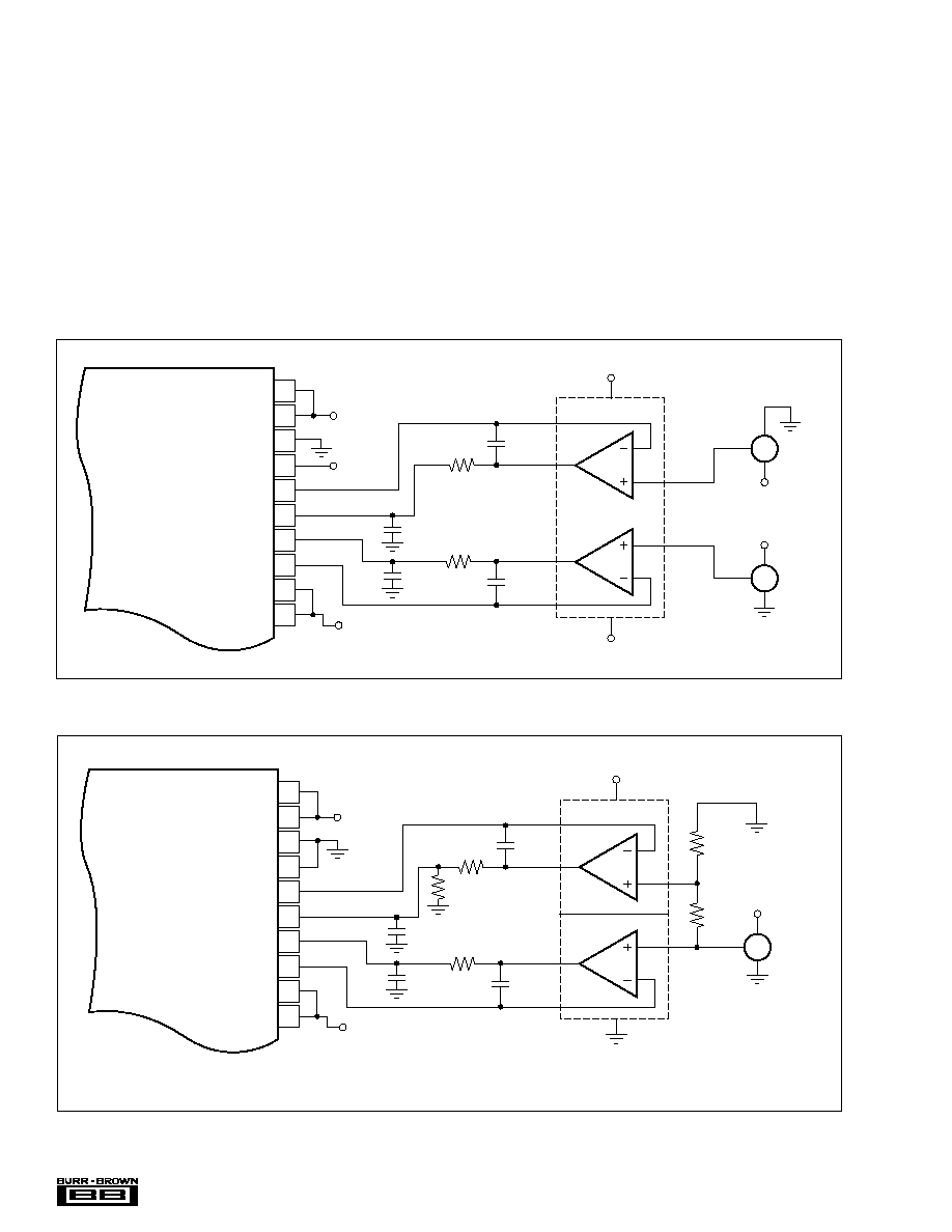
FIGURE 5. Dual Supply Configuration-Buffered References, used for Dual Supply Performance (1/2 DAC7734).
FIGURE 6. Single-Supply Buffered Reference with a Reference Low of 50mV used for Single-Supply Performance Curves
(1/2 DAC7734).
+10V
+V
≠10V
≠V
V
OUT
≠15V
V
OUT
V
OUT
A Sense
V
OUT
A
AGND
V
SS
V
REF
L AB Sense
V
REF
L AB
V
REF
H AB
V
REF
H AB Sense
V
OUT
B Sense
V
OUT
B
48
47
46
45
44
43
42
41
40
39
DAC7734
2200pF
100
1000pF
1000pF
2200pF
+V
OPA2234
≠V
100
V
OUT
V
OUT
A Sense
V
OUT
A
AGND
V
SS
V
REF
L AB Sense
V
REF
L AB
V
REF
H AB
V
REF
H AB Sense
V
OUT
B Sense
V
OUT
B
48
47
46
45
44
43
42
41
40
39
DAC7734
+10V
+V
OPA350
OPA227
99.5k
+0.050V
500
50
V
OUT
NOTE: V
REF
L has been chosen to be 50mV to allow for current sinking voltage drops across the 100
resistor and the output stage of the buffer op amp.
2200pF
100
1000pF
1000pF
2200pF
+V
100

19
Æ
DAC7734
FIGURE 8. Dual-Supply Buffered Reference with V
REF
L = ≠5V and V
REF
H = +5V (1/2 DAC7734).
+5V
+V
≠5V
≠V
V
OUT
V
OUT
A Sense
V
OUT
A
AGND
V
SS
V
REF
L AB Sense
V
REF
L AB
V
REF
H AB
V
REF
H AB Sense
V
OUT
B Sense
V
OUT
B
48
47
46
45
44
43
42
41
40
39
DAC7734
OPA2234
V
OUT
2200pF
100
1000pF
1000pF
2200pF
+V
≠V
100
FIGURE 7. Integral Linearity and Differential Linearity Error Curves for Figure 8.
2.0
1.5
1.0
0.5
0
≠0.5
≠1.0
≠1.5
≠2.0
LE (LSB)
LINEARITY ERROR AND
DIFFERENTIAL LINEARITY ERROR vs CODE
(DAC A, 25
∞
C)
0000
H
2000
H
4000
H
6000
H
8000
H
Digital Input Code
A000
H
C000
H
E000
H
FFFF
H
2.0
1.5
1.0
0.5
0
≠0.5
≠1.0
≠1.5
≠2.0
DLE (LSB)
2.0
1.5
1.0
0.5
0
≠0.5
≠1.0
≠1.5
≠2.0
LE (LSB)
LINEARITY ERROR AND
DIFFERENTIAL LINEARITY ERROR vs CODE
(DAC B, 25
∞
C)
0000
H
2000
H
4000
H
6000
H
8000
H
Digital Input Code
A000
H
C000
H
E000
H
FFFF
H
2.0
1.5
1.0
0.5
0
≠0.5
≠1.0
≠1.5
≠2.0
DLE (LSB)
2.0
1.5
1.0
0.5
0
≠0.5
≠1.0
≠1.5
≠2.0
LE (LSB)
LINEARITY ERROR AND
DIFFERENTIAL LINEARITY ERROR vs CODE
(DAC C, 25
∞
C)
0000
H
2000
H
4000
H
6000
H
8000
H
Digital Input Code
A000
H
C000
H
E000
H
FFFF
H
2.0
1.5
1.0
0.5
0
≠0.5
≠1.0
≠1.5
≠2.0
DLE (LSB)
2.0
1.5
1.0
0.5
0
≠0.5
≠1.0
≠1.5
≠2.0
LE (LSB)
LINEARITY ERROR AND
DIFFERENTIAL LINEARITY ERROR vs CODE
(DAC D, 25
∞
C)
0000
H
2000
H
4000
H
6000
H
8000
H
Digital Input Code
A000
H
C000
H
E000
H
FFFF
H
2.0
1.5
1.0
0.5
0
≠0.5
≠1.0
≠1.5
≠2.0
DLE (LSB)

20
Æ
DAC7734
FIGURE 9. Single-Supply Buffered Reference with a Reference Low of 50mV and Reference High of +5V.
V
OUT
A Sense
V
OUT
A
AGND
V
SS
V
REF
L AB Sense
V
REF
L AB
V
REF
H AB
V
REF
H AB Sense
V
OUT
B Sense
V
OUT
B
48
47
46
45
44
43
42
41
40
39
DAC7734
V
OUT
V
OUT
99k
0.05V
1k
+5V
+V
1000pF
2200pF
+V
OPA350
OPA227
100
1000pF
2200pF
100
NOTE: V
REF
L has been chosen to be 50mV to allow for current sinking voltage drops across the 100
resistor and the output stage of the buffer op amp.
50
FIGURE 10. Integral Linearity and Differential Linearity Error Curves for Figure 9.
2.0
1.5
1.0
0.5
0
≠0.5
≠1.0
≠1.5
≠2.0
LE (LSB)
LINEARITY ERROR AND
DIFFERENTIAL LINEARITY ERROR vs CODE
(DAC A, 25
∞
C)
0000
H
2000
H
4000
H
6000
H
8000
H
Digital Input Code
A000
H
C000
H
E000
H
FFFF
H
2.0
1.5
1.0
0.5
0
≠0.5
≠1.0
≠1.5
≠2.0
DLE (LSB)
2.0
1.5
1.0
0.5
0
≠0.5
≠1.0
≠1.5
≠2.0
LE (LSB)
LINEARITY ERROR AND
DIFFERENTIAL LINEARITY ERROR vs CODE
(DAC B, 25
∞
C)
0000
H
2000
H
4000
H
6000
H
8000
H
Digital Input Code
A000
H
C000
H
E000
H
FFFF
H
2.0
1.5
1.0
0.5
0
≠0.5
≠1.0
≠1.5
≠2.0
DLE (LSB)
2.0
1.5
1.0
0.5
0
≠0.5
≠1.0
≠1.5
≠2.0
LE (LSB)
LINEARITY ERROR AND
DIFFERENTIAL LINEARITY ERROR vs CODE
(DAC C, 25
∞
C)
0000
H
2000
H
4000
H
6000
H
8000
H
Digital Input Code
A000
H
C000
H
E000
H
FFFF
H
2.0
1.5
1.0
0.5
0
≠0.5
≠1.0
≠1.5
≠2.0
DLE (LSB)
2.0
1.5
1.0
0.5
0
≠0.5
≠1.0
≠1.5
≠2.0
LE (LSB)
LINEARITY ERROR AND
DIFFERENTIAL LINEARITY ERROR vs CODE
(DAC D, 25
∞
C)
0000
H
2000
H
4000
H
6000
H
8000
H
Digital Input Code
A000
H
C000
H
E000
H
FFFF
H
2.0
1.5
1.0
0.5
0
≠0.5
≠1.0
≠1.5
≠2.0
DLE (LSB)

21
Æ
DAC7734
INPUT
DAC
A1
A0
CS
RST
RSTSEL
LDAC
LOAD
REGISTER
REGISTER
MODE
DAC
L
L
L
H
X
X
L
Write
Hold
Write Input
A
L
H
L
H
X
X
L
Write
Hold
Write Input
B
H
L
L
H
X
X
L
Write
Hold
Write Input
C
H
H
L
H
X
X
L
Write
Hold
Write Input
D
X
X
H
H
X
H
Hold
Write
Update
All
X
X
H
H
X
H
H
Hold
Hold
Hold
All
X
X
X
L
X
X
Reset to Zero
Reset to Zero
Reset to Zero
All
X
X
X
H
X
X
Reset to Midscale
Reset to Midscale
Reset to Midscale
All
TABLE I. DAC7734 Logic Truth Table.
DIGITAL INTERFACE
Table I shows the basic control logic for the DAC7734. The
interface consists of a Signal Data Clock (CLK) input, Serial
Data (SDI), DAC Input Register Load Control Signal
(LOAD), and DAC Register Load Control Signal (LDAC).
In addition, a Chip Select (CS) input is available to enable
serial communication when there are multiple serial devices.
An asynchronous Reset (RST) input, by the rising edge, is
provided to simplify start-up conditions, periodic resets, or
emergency resets to a known state, depending on the status
of the reset select (RSTSEL) signal.
The DAC code, quick load control, and address are provided
via a 24-bit serial interface (see Table I). The first two bits
shifted into the shift register, B23 and B22, are the DAC
register address. These bits select the input register that will
be updated when LOAD goes LOW. The third bit, B21, is a
"Quick Load" bit such that if HIGH, the code in the shift
register is loaded into ALL DAC input registers when the
LOAD signal goes LOW, independent of the state of the
address bits, B23 and B22. If the "Quick Load" bit is LOW,
the contents of the shift register is loaded only to the DAC
register that is addressed. Bits B20 through B16 are not used
and can assume any logical value. The last sixteen bits, B15
through B0, make up the DAC code to be loaded into the
selected input register.
The internal DAC register is edge triggered and not level
triggered. When the LDAC signal is transitioned from LOW
to HIGH, the digital word currently in the DAC input
register is latched. The first set of registers (the DAC input
registers) are level triggered via the LOAD signal. This
double-buffered architecture has been designed so that new
data can be entered for each DAC without disturbing the
analog outputs. When the new data has been entered into the
B23
B22
B21
B20
B19
B18
B17
B16
B15
B14
B13
B12
B11
B10
B9
B8
B7
B6
B5
B4
B3
B2
B1
B0
A1
A0
X
X
X
X
X
D15
D14
D13
D12
D11
D10
D9
D8
D7
D6
D5
D4
D3
D2
D1
D0
QUICK
LOAD
SERIAL DATA INPUT
device, all of the DAC outputs can be updated simulta-
neously by the rising edge of LDAC. Additionally, it allows
the DAC input registers to be written to at any point, then the
DAC output voltages can be synchronously changed via a
trigger signal (LDAC).
Note that CS and CLK are combined with an OR gate, which
controls the serial-to-parallel shift register. These two inputs
are completely interchangeable. In addition, care must be
taken with the state of CLK when CS rises at the end of a
serial transfer. If CLK is LOW when CS rises, the OR gate
will provide a rising edge to the shift register, shifting the
internal data one additional bit. The result will be incorrect
data and possible selection of the wrong input register(s). If
both CS and CLK are used, CS should rise only when CLK
is HIGH. If not, then either CS or CLK can be used to
operate the shift register. See Table II for more information.
CS
(1)
CLK
(1)
LOAD
RST
SERIAL SHIFT REGISTER
H
(2)
X
(3)
H
H
No Change
L
(4)
L
H
H
No Change
L
(5)
H
H
Advanced One Bit
L
H
H
Advanced One Bit
H
(6)
X
L
(7)
H
No Change
H
(6)
X
H
(8)
No Change
NOTES: (1) CS and CLK are interchangeable. (2) H = Logic HIGH.
(3) X = Don't Care. (4) L = Logic LOW (5) = Positive Logic Transition.
(6) A HIGH value is suggested in order to avoid a "false clock" from advancing
the shift register and changing the shift register. (7) If data is clocked into the
serial register while LOAD is LOW, the selected DAC register will change as
the shift register bits "flow" through A1 and A0. This will corrupt the data in
each DAC register that has been erroneously selected. (8) Rising edge of RST
causes no change in the contents of the serial shift register.
TABLE II. Serial Shift Register Truth Table.
22
Æ
DAC7734
(1)
V
V
L
V
H
V
L
N
OUT
REF
REF
REF
=
+
(
)
≠
∑
,
65 536
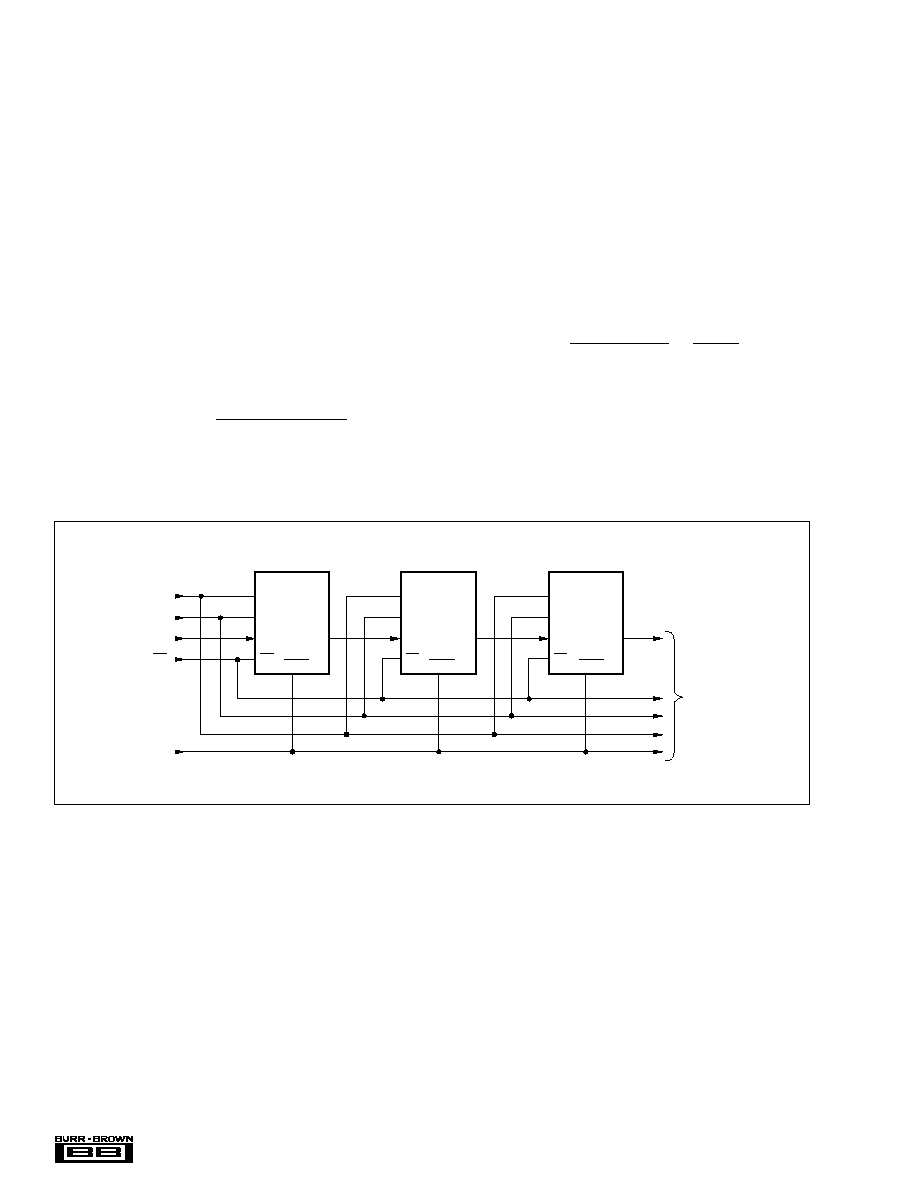
FIGURE 11. Daisy-Chaining DAC7734.
SERIAL-DATA OUTPUT
The Serial-Data Output (SDO) is the internal shift register's
output. For DAC7734, the SDO is a driven output and does
not require an external pull-up. Any number of DAC7734's
can be daisy chained by connecting the SDO pin of one
device to the SDI pin of the following device in the chain,
as shown in Figure 11.
DIGITAL TIMING
Figure 12 and Table III provide detailed timing for the
digital interface of the DAC7734.
DIGITAL INPUT CODING
The DAC7734 input data is in Straight Binary format. The
output voltage is given by Equation 1.
where N is the digital input code. This equation does not
(2)
I
V
H
V
L
R
V
L R
OUT
REF
REF
SENSE
REF
SENSE
=
+
(
)
≠
∑
,
/
N
65 536
DIGITALLY-PROGRAMMABLE
CURRENT SOURCE
The DAC7734 offers a unique set of features that allows a
wide range of flexibility in designing applications circuits
such as programmable current sources. The DAC7734 offers
both a differential reference input, as well as an open-loop
configuration around the output amplifier. The open-loop
configuration around the output amplifier allows a transistor
to be placed within the loop to implement a digitally-
programmable, unidirectional current source. The availabil-
ity of a differential reference allows programmability for
both the full-scale and zero-scale currents. The output cur-
rent is calculated as:
include the effects of offset (zero-scale) or gain (full-scale)
errors.
DAC7734
CLK
SDI
CS
SCK
DIN
CS
LDAC
SDO
DAC7734
CLK
SDI
CS
SDO
LOAD
DAC7734
LOAD
LOAD
LOAD
CLK
SDI
CS
LDAC
LDAC
LDAC
SDO
To
Other
Serial
Devices
23
Æ
DAC7734
SYMBOL
DESCRIPTION
MIN
MAX
UNITS
t
DS
Data Valid to CLK Rising
10
ns
t
DH
Data Held Valid after CLK Rises
20
ns
t
CH
CLK HIGH
25
ns
t
CL
CLK LOW
25
ns
t
CSS
CS LOW to CLK Rising
15
ns
t
CSH
CLK HIGH to CS Rising
0
ns
t
LD1
LOAD HIGH to CLK Rising
10
ns
t
LD2
CLK Rising to LOAD LOW
30
ns
t
LDRW
LOAD LOW Time
30
ns
t
LDDWL
LDAC LOW Time
40
ns
t
LDDH
LDAC HIGH Time
40
ns
t
SDO
SDO Propagation Delay
10
45
ns
t
RSSS
RESETSEL Valid to RESET HIGH
0
ns
t
RSSH
RESET HIGH to RESETSEL Not Valid
100
ns
t
RSTL
RESET LOW Time
10
ns
t
RSTH
RESET HIGH Time
10
ns
t
LDDD
LOAD LOW to LDAC Rising Time
40
ns
t
S
Settling Time
10 (dual)/11(single)
µ
s
TABLE III. Timing Specifications (T
A
= ≠40
∞
C to +85
∞
C).
FIGURE 12. Digital Input and Output Timing.
A1
(LSB)
SDI
CLK
CS
LOAD
A0
D3
D2
D1
D0
SDI
CLK
LDAC
RESET
V
OUT
tcss
t
LD1
t
CL
t
SDO
t
CH
t
DS
t
DH
t
LD2
t
LDRW
t
S
t
RSTH
t
RSTL
t
RSSS
t
RSSH
SDO
t
CSH
t
S
±
0.003%
ERROR BAND
±
0.003%
ERROR BAND
RESETSEL
D15
D14
D13
XXXXX
QUICK
LOAD
(MSB)
t
LDDD
LDAC
t
LDDH
t
LDDL
24
Æ
DAC7734
(3)
FIGURE 13. 4-to-20mA Digitally Controlled Current Source (1/2 DAC7734).
I
OUT
V
PROGRAMMED
R
SENSE
250
I
OUT
V
PROGRAMMED
R
SENSE
250
V
OUT
A Sense
V
OUT
A
AGND
V
SS
V
REF
L AB Sense
V
REF
L AB
V
REF
H AB
V
REF
H AB Sense
V
OUT
B Sense
V
OUT
B
48
47
46
45
44
43
42
41
40
39
DAC7734
5V
OPA2350
80k
20k
1.0V
2200pF
100
1000pF
1000pF
2200pF
+V
+V
100
I
V
V
N
V
OUT
=
+
5
1
250
65 536
1
250
≠
∑
,
Figure 13 shows a DAC7734 in a 4mA to 20mA current
output configuration. The output current can be determined
by Equation 3:
At full-scale, the output current is 16mA, plus the 4mA, for
the zero current. At zero scale the output current is the offset
current of 4mA (1V/250
).