Burr Brown Products
from Texas Instruments
DAC7822
FEATURES
DESCRIPTION
APPLICATIONS
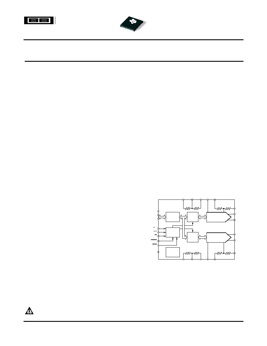
12-Bit
R-2R DAC A
12-Bit
R-2R DAC B
LATCH
R A
FB
I
1A
OUT
I
2A
OUT
I
1B
OUT
DAC /B
A
CS
R/W
V
DD
DB0
DATA
INPUTS
DB11
LDAC
CLR
I
2B
OUT
LATCH
INPUT
BUFFER
CONTROL
LOGIC
R
1
2R
R
FB
2R
R
3
2R
R A
3
R
A
2_3
R A
2
V
A
REF
R A
1
R
2
2R
R
3
2R
R
2
2R
GND
POWER-ON
RESET
R B
3
R
B
2_3
R B
2
V
B
REF
R B
1
R
FB
B
R
1
2R
R
FB
2R
DAC7822
SBAS374 ≠ JUNE 2006
Dual, 12-Bit, Parallel Input, Multiplying
Digital-to-Analog Converter
∑
±
1LSB INL
The DAC7822 is a dual, CMOS, 12-bit, current
output digital-to-analog converter (DAC). This device
∑
2.5V to 5.5V Supply Operation
operates from a 2.5V to 5.5V power supply, making it
∑
Fast Parallel Interface:
suitable
for
battery-powered
and
many
other
17ns Write Cycle
applications.
∑
Update Rate of 20.4MSPS
The DAC7822 operates with a fast parallel interface.
∑
10MHz Multiplying Bandwidth
Data readback allows the user to read the contents
∑
±
15V Reference Input
of the DAC register via the DB pins. On power-up,
the internal register and latches are filled with zeroes
∑
Extended Temperature Range:
and the DAC outputs are at zero scale.
≠40
∞
C to +125
∞
C
The
DAC7822
offers
excellent
4-quadrant
∑
40-Lead QFN
multiplication
characteristics,
with
large
signal
∑
12-Bit Monotonic
multiplying
bandwidth
of
10MHz.
The
applied
∑
4-Quadrant Multiplication
external reference input voltage (V
REF
) determines
∑
Power-On Reset with Brownout Detection
the full-scale output current. An integrated feedback
resistor (R
FB
) provides temperature tracking and
∑
Readback Function
full-scale voltage output when combined with an
∑
Industry-Standard Pin Configuration
external current-to-voltage precision amplifier. The
∑
Pin-Compatible with the AD5405
DAC7822 also includes the resistors necessary for
4-quadrant multiplication and other configuration
modes.
∑
Portable Battery-Powered Instruments
The DAC7822 is available in a 40-lead QFN
∑
Waveform Generators
package.
∑
Analog Processing
∑
Programmable Amplifiers and Attenuators
∑
Digitally-Controlled Calibration
∑
Programmable Filters and Oscillators
∑
Ultrasound
Please be aware that an important notice concerning availability, standard warranty, and use in critical applications of Texas
Instruments semiconductor products and disclaimers thereto appears at the end of this data sheet.
All trademarks are the property of their respective owners.
PRODUCTION DATA information is current as of publication date.
Copyright © 2006, Texas Instruments Incorporated
Products conform to specifications per the terms of the Texas
Instruments standard warranty. Production processing does not
necessarily include testing of all parameters.
www.ti.com
ABSOLUTE MAXIMUM RATINGS
DAC7822
SBAS374 ≠ JUNE 2006
This integrated circuit can be damaged by ESD. Texas Instruments recommends that all integrated circuits be handled with
appropriate precautions. Failure to observe proper handling and installation procedures can cause damage.
ESD damage can range from subtle performance degradation to complete device failure. Precision integrated circuits may be
more susceptible to damage because very small parametric changes could cause the device not to meet its published
specifications.
ORDERING INFORMATION
(1)
SPECIFIED
PACKAGE
TEMPERATURE
PACKAGE
ORDERING
TRANSPORT MEDIA,
PRODUCT
PACKAGE
DESIGNATOR
RANGE
MARKING
NUMBER
QUANTITY
DAC7822IRTAT
250, Tape and Reel
DAC7822
40-QFN
RTA
≠40
∞
C to +125
∞
C
DAC7822
DAC7822IRTAR
2000, Tape and Reel
(1)
For the most current specifications and package information, see the Package Option Addendum at the end of this data sheet, or refer
to our web site at
www.ti.com
.
over operating free-air temperature range (unless otherwise noted)
(1)
DAC7822
UNIT
V
DD
to GND
≠0.3 to +7.0
V
Digital input voltage to GND
≠0.3 to V
DD
+ 0.3
V
V
OUT
to GND
≠0.3 to V
DD
+ 0.3
V
Operating temperature range
≠40 to +125
∞
C
Storage temperature range
≠65 to +150
∞
C
Junction temperature (T
J
max)
+150
∞
C
ESD Rating, HBM
2000
V
ESD Rating, CDM
1000
V
(1)
Stresses above those listed under absolute maximum ratings may cause permanent damage to the device. Exposure to absolute
maximum conditions for extended periods may affect device reliability.
2
Submit Documentation Feedback

www.ti.com
ELECTRICAL CHARACTERISTICS
DAC7822
SBAS374 ≠ JUNE 2006
V
DD
= +2.5V to +5.5V; I
OUT
1 = Virtual GND; I
OUT
2 = 0V; V
REF
= 10V; T
A
= full operating temperature. All specifications ≠40
∞
C
to +125
∞
C, unless otherwise noted.
DAC7822
PARAMETER
CONDITIONS
MIN
TYP
MAX
UNITS
STATIC PERFORMANCE
Resolution
12
Bits
Relative accuracy
±
1
LSB
Differential nonlinearity
±
1
LSB
Output leakage current
Data = 000h, T
A
= +25
∞
C
±
1
nA
Output leakage current
Data = 000h, T
A
= T
MAX
±
15
nA
Full-scale gain error
All ones loaded to DAC register
±
10
±
25
mV
Full-scale tempco
(1)
±
5
ppm/
∞
C
Bipolar zero-code error
Circuit configuration as shown in
Figure 41
±
25
mV
Output capacitance
DAC latches leaded with all 1s
25
30
pF
REFERENCE INPUT
V
REF
range
≠15
15
V
V
REF
A, V
REF
B, Input resistance
8
10
12
k
R
1
, R
FB
resistance
17
20
25
k
R
2
, R
3
resistance
17
20
25
k
V
REF
A to V
REF
B Input Mismatch
1.6
2.5
%
R
2
to R
3
Mismatch
0.06
0.18
%
LOGIC INPUTS AND OUTPUT
(1)
V
DD
= +2.5V
0.6
V
Input low voltage
V
IL
V
DD
= +5V
0.8
V
V
DD
= +2.5V
2.1
V
Input high voltage
V
IH
V
DD
= +5V
2.4
V
Input leakage current
I
IL
1
µA
Input capacitance
C
IL
10
pF
POWER REQUIREMENTS
V
DD
2.5
5.5
V
I
DD
(normal operation)
Logic inputs = 0V
5
µA
V
DD
= +4.5V to +5.5V
V
IH
= V
DD
and V
IL
= GND
0.8
5
µA
V
DD
= +2.5V to +3.6V
V
IH
= V
DD
and V
IL
= GND
0.4
2.5
µA
AC CHARACTERISTICS
(1)
Output voltage settling time
0.2
µs
Reference multiplying BW
V
REF
= 7V
PP
, Data = FFFh
10
MHz
V
REF
= 0V to 10V,
DAC glitch impulse
10
nV-s
Data = 7FFh to 800h to 7FFh
Feedthrough error V
OUT
/V
REF
Data = 000h, V
REF
= 100kHz
≠70
dB
Digital feedthrough
2
nV-s
Total harmonic distortion
≠105
dB
Output spot noise voltage
25
nV/
Hz
(1)
Specified by design and characterization; not production tested.
3
Submit Documentation Feedback

www.ti.com
t
1
R/W
t
2
t
8
CS
DACA/DACB
t
3
t
t
4
t
6
t
7
t
13
t
12
t
10
t
11
t
5
t
2
DATA
9
DATA VALID
DATA VALID
TIMING REQUIREMENTS: 2.5 V to 5.5 V
DAC7822
SBAS374 ≠ JUNE 2006
TIMING INFORMATION
At t
r
= t
f
= 1ns (10% to 90% of V
DD
) and timed from a voltage level of (V
IL
+ V
IH
)/2; V
DD
= 2.5V to 5.5V, V
REF
= 10V,
I
OUT
2 = 0V. All specifications ≠40
∞
C to +125
∞
C, unless otherwise noted.
DAC7822
PARAMETER
(1)
TEST CONDITIONS
MIN
TYP
MAX
UNIT
t
1
R/W to CS setup time
0
ns
t
2
R/W to CS hold time
0
ns
t
3
CS low time (write cycle)
10
ns
t
4
Address setup time
10
ns
t
5
Address hold time
0
ns
t
6
Data setup time
6
ns
t
7
Data hold time
0
ns
t
8
R/W high to CS low
5
ns
t
9
CS minimum high time
7
ns
t
10
Address setup time (Read Cycle)
0
ns
t
11
Address hold time (Read Cycle)
0
ns
t
12
Data access time
5
35
ns
t
13
Bus relinquish time
5
10
ns
(1)
Ensured by design; not production tested.
4
Submit Documentation Feedback

www.ti.com
DEVICE INFORMATION
R A
1
R A
2
R
A
2_3
R A
3
V
A
REF
DGND
LDAC
DAC A/B
NC
DB11
R B
1
R B
2
R
B
2_3
R B
3
V
B
REF
V
DD
CLR
R/W
CS
DB0
1
2
3
4
5
6
7
8
9
10
30
29
28
27
26
25
24
23
22
21
DAC7822
11
12
13
14
15
16
17
18
19
20
DB10
DB9
DB8
DB7
DB6
DB5
DB4
DB3
DB2
DB1
40
39
38
37
36
35
34
33
32
31
R
A
F
B
I
2A
O
U
T
I
1A
O
U
T
NC
NC
NC
NC
I
1B
O
U
T
I
2B
O
U
T
R
B
F
B
DAC7822
SBAS374 ≠ JUNE 2006
TERMINAL FUNCTIONS
PIN NO.
PIN NAME
DESCRIPTION
DAC A 4-Quadrant Resistors. Allows a number of configuration modes, including bipolar operation with
1-4
R
1
A, R
2
A, R
2_3
A, R
3
A
minimum of external components.
5, 26
V
REF
A, V
REF
B
DAC Reference Voltage Input Terminals.
6
DGND
Digital Ground Pin.
Load DAC Input. Allows asynchronous or synchronous updates to the DAC output. The DAC is asynchronously
7
LDAC
updated when this signal goes low. Alternatively, if this line is held permanently low, an automatic or
synchronous update mode is selected whereby the DAC is updated on the rising edge of CS.
8
DAC A/B
Selects DAC A or B. Low selects DAC A, and high selects DAC B.
9, 34-37
NC
Not internally connected.
10-21
DB11 to DB0
Parallel Data Bits 11 through 0.
Chip Select Input; active low. Used in conjuction with R/W to load parallel data to the input latch or to read data
22
CS
from the DAC register. Edge sensitive; when pulled high, the DAC data is latched.
Read/Write. When low, used in conjunction with CS to load parallel data. When high, used in conjunction with
23
R/W
CS to read back contents of DAC register.
24
CLR
Active Low Control Input. Clears DAC output and input and DAC registers.
25
V
DD
Positive Power Supply Input. These parts can be operated from a supply of 2.5V to 5.5V.
DAC B 4-Quadrant Resistors. Allow a number of configuration modes, including bipolar operation with a
27-30
R
3
B, R
2_3
B, R
2
B, R
1
B
minimum of external components.
31, 40
R
FB
B, R
FB
A
External Amplifier Output.
DAC A Analog Ground. This pin typically should be tied to the analog ground of the system, but can be biased
32
I
OUT
2B
to achieve single-supply operation.
33
I
OUT
1B
DAC B Current Output.
38
I
OUT
1A
DAC A Current Output.
DAC A Analog Ground. This pin typically should be tied to the analog ground of the system, but can be biased
39
I
OUT
2A
to achieve single-supply operation.
5
Submit Documentation Feedback