Document Outline
- FEATURES
- APPLICATIONS
- DESCRIPTION
- ABSOLUTE MAXIMUM RATINGS
- PACKAGE/ORDERING INFORMATION
- ELECTRICAL CHARACTERISTICS
- PIN CONFIGURATION
- PIN DESCRIPTIONS
- TIMING CHARACTERISTICS
- SERIAL WRITE OPERATION
- TYPICAL CHARACTERISTICS
- THEORY OF OPERATION
- DAC SECTION
- RESISTOR STRING
- OUTPUT AMPLIFIER
- SERIAL INTERFACE
- INPUT SHIFT REGISTER
- SYNC\ INTERRUPT
- POWER-ON RESET
- POWER-DOWN MODES
- OPERATION EXAMPLES
- MICROPROCESSOR INTERFACING
- DAC8532 to 8051 INTERFACE
- DAC8532 to Microwire INTERFACE
- DAC8532 to 68HC11 INTERFACE
- DAC8532 to TMS320 DSP INTERFACE
- APPLICATIONS
- CURRENT CONSUMPTION
- DRIVING RESISTIVE AND CAPACITIVE LOADS
- CROSSTALK AND AC PERFORMANCE
- OUTPUT VOLTAGE STABILITY
- SETTLING TIME AND OUTPUT GLITCH PERFORMANCE
- USING REF02 AS A POWER SUPPLY FOR DAC8532
- BIPOLAR OPERATION USING THE DAC8532
- LAYOUT
- PACKAGE DRAWING
- DGK (R-PDSO-G8) PLASTIC SMALL-OUTLINE PACKAGE
Dual Channel, Low Power, 16-Bit, Serial Input
DIGITAL-TO-ANALOG CONVERTER
APPLICATIONS
q
PORTABLE INSTRUMENTATION
q
CLOSED-LOOP SERVO-CONTROL
q
PROCESS CONTROL
q
DATA ACQUISITION SYSTEMS
q
PROGRAMMABLE ATTENUATION
q
PC PERIPHERALS
DESCRIPTION
The DAC8532 is a dual channel, 16-bit Digital-to-Analog
Converter (DAC) offering low power operation and a flexible
serial host interface. Each on-chip precision output amplifier
allows rail-to-rail output swing to be achieved over the supply
range of 2.7V to 5.5V. The device supports a standard 3-wire
serial interface capable of operating with input data clock
frequencies up to 30MHz for V
DD
= 5V.
The DAC8532 requires an external reference voltage to set
the output range of each DAC channel. Also incorporated
into the device is a power-on reset circuit which ensures that
the DAC outputs power up at zero-scale and remain there
until a valid write takes place. The DAC8532 provides a
flexible power-down feature, accessed over the serial inter-
face, that reduces the current consumption of the device to
200nA at 5V.
The low-power consumption of this device in normal opera-
tion makes it ideally suited to portable battery-operated
equipment and other low-power applications. The power
consumption is 2.5mW at 5V, reducing to 1
�
W in power-
down mode.
The DAC8532 is available in a MSOP-8 package with a
specified operating temperature range of �40
�
C to +105
�
C.
FEATURES
q
microPOWER OPERATION: 500
�
A at 5V
q
POWER-ON RESET TO ZERO-SCALE
q
POWER SUPPLY: +2.7V to +5.5V
q
16-BIT MONOTONIC OVER TEMPERATURE
q
SETTLING TIME: 10
�
s to
�
0.003% FSR
q
ULTRA-LOW AC CROSSTALK: �100dB typ
q
LOW-POWER SERIAL INTERFACE WITH
SCHMITT-TRIGGERED INPUTS
q
ON-CHIP OUTPUT BUFFER AMPLIFIER WITH
RAIL-TO-RAIL OPERATION
q
DOUBLE BUFFERED INPUT ARCHITECTURE
q
SIMULTANEOUS OR SEQUENTIAL OUTPUT
UPDATE AND POWERDOWN
q
TINY MSOP-8 PACKAGE
DAC8532
SBAS246A � DECEMBER 2001 � MAY 2003
www.ti.com
Copyright � 2001-2003, Texas Instruments Incorporated
Please be aware that an important notice concerning availability, standard warranty, and use in critical applications of
Texas Instruments semiconductor products and disclaimers thereto appears at the end of this data sheet.
PRODUCTION DATA information is current as of publication date.
Products conform to specifications per the terms of Texas Instruments
standard warranty. Production processing does not necessarily include
testing of all parameters.
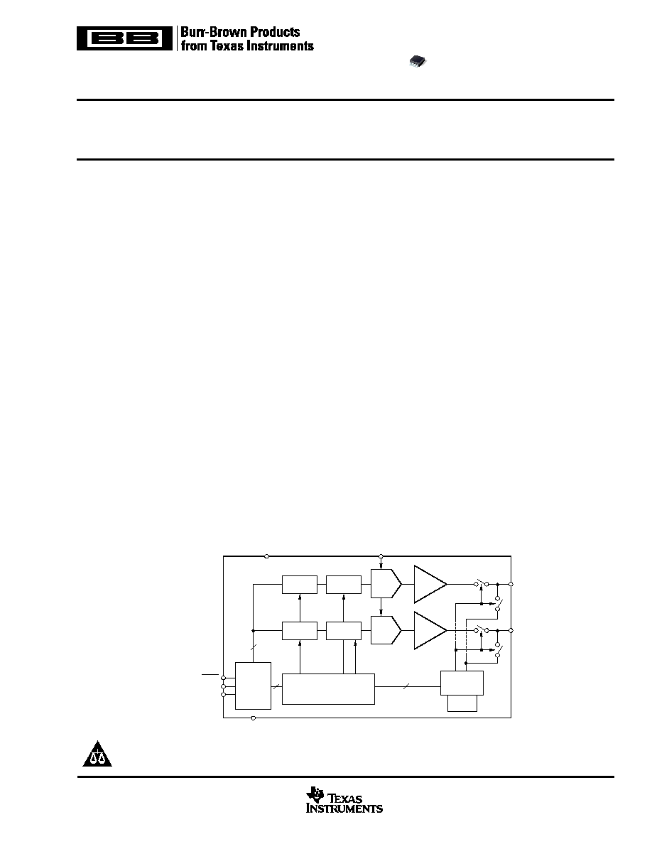
Control Logic
Channel
Select
Load
Control
8
Data
Buffer B
DAC
Register B
16
DAC B
Power-Down
Control Logic
24-Bit
Serial-to-
Parallel
Shift
Register
Resistor
Network
V
DD
GND
V
OUT
A
V
OUT
B
Data
Buffer A
DAC
Register A
DAC A
V
REF
SYNC
2
SCLK
D
IN
DAC8532
2
SBAS246A
www.ti.com
SPECIFICATION
PACKAGE
TEMPERATURE
PACKAGE
ORDERING
TRANSPORT
PRODUCT
PACKAGE-LEAD
DESIGNATOR
(1)
RANGE
MARKING
NUMBER
MEDIA, QUANTITY
DAC8532
MSOP-8
DGK
�40
�
C to +105
�
C
D32E
DAC8532IDGK
Tube, 80
"
"
"
"
DAC8532IDGKR
Tape and Reel,
2500
NOTE: (1) For the most current specifications and package information, refer to our web site at www.ti.com.
PARAMETER
CONDITIONS
MIN
TYP
MAX
UNITS
STATIC PERFORMANCE
(1)
Resolution
16
Bits
Relative Accuracy
�
0.0987
% of FSR
Differential Nonlinearity
16-Bit Monotonic
�
1
LSB
Zero-Scale Error
+5
+25
mV
Full-Scale Error
�0.15
�1.0
% of FSR
Gain Error
�
1.0
% of FSR
Zero-Scale Error Drift
�
20
�
V/
�
C
Gain Temperature Coefficient
�
5
ppm of FSR/
�
C
Channel-to-Channel Matching
R
L
= 2k
, C
L
= 200pF
15
mV
PSRR
0.75
mV/V
OUTPUT CHARACTERISTICS
(2)
Output Voltage Range
0
V
REF
V
Output Voltage Settling Time
To
�
0.003% FSR
0200
H
to FD00
H
8
10
�
s
R
L
= 2k
; 0pF < C
L
< 200pF
R
L
= 2k
; C
L
= 500pF
12
�
s
Slew Rate
1
V/
�
s
Capacitive Load Stability
R
L
=
470
pF
R
L
= 2k
1000
pF
Code Change Glitch Impulse
1LSB Change Around Major Carry
20
nV-s
Digital Feedthrough
0.5
nV-s
DC Crosstalk
0.25
LSB
AC Crosstalk
�100
�96
dB
DC Output Impedance
1
Short-Circuit Current
V
DD
= +5V
50
mA
V
DD
= +3V
20
mA
Power-Up Time
Coming Out of Power-Down Mode
V
DD
= +5V
2.5
�
s
Coming Out of Power-Down Mode
V
DD
= +3V
5
�
s
AC PERFORMANCE
BW = 20kHz, V
DD
= 5V
F
OUT
= 1kHz, 1st 19 Harmonics Removed
SNR
94
dB
THD
67
dB
SFDR
69
dB
SINAD
65
dB
V
DD
to GND ........................................................................... �0.3V to +6V
Digital Input Voltage to GND ................................. �0.3V to +V
DD
+ 0.3V
V
OUTA
or V
OUTB
to GND .......................................... �0.3V to +V
DD
+ 0.3V
Operating Temperature Range ...................................... �40
�
C to +105
�
C
Storage Temperature Range ......................................... �65
�
C to +150
�
C
Junction Temperature Range (T
J
max) ........................................ +150
�
C
Power Dissipation ........................................................ (T
J
max -- T
A
)/
JA
JA
Thermal Impedance ......................................................... 206
�
C/W
JC
Thermal Impedance .......................................................... 44
�
C/W
Lead Temperature, Soldering:
Vapor Phase (60s) ............................................................... +215
�
C
Infrared (15s) ........................................................................ +220
�
C
NOTE: (1) Stresses above those listed under "Absolute Maximum Ratings"
may cause permanent damage to the device. Exposure to absolute maximum
conditions for extended periods may affect device reliability.
ELECTROSTATIC
DISCHARGE SENSITIVITY
This integrated circuit can be damaged by ESD. Texas Instru-
ments recommends that all integrated circuits be handled with
appropriate precautions. Failure to observe proper handling
and installation procedures can cause damage.
ESD damage can range from subtle performance degradation
to complete device failure. Precision integrated circuits may be
more susceptible to damage because very small parametric
changes could cause the device not to meet its published
specifications.
ABSOLUTE MAXIMUM RATINGS
(1)
PACKAGE/ORDERING INFORMATION
ELECTRICAL CHARACTERISTICS
V
DD
= +2.7V to +5.5V. �40
�
C to +105
�
C, unless otherwise specified.
DAC8532
3
DAC8532
SBAS246A
www.ti.com
REFERENCE INPUT
Reference Current
V
REF
= V
DD
= +5V
67
90
�
A
V
REF
= V
DD
= +3V
40
54
�
A
Reference Input Range
0
V
DD
V
Reference Input Impedance
75
k
LOGIC INPUTS
(2)
Input Current
�
1
�
A
V
IN
L, Input LOW Voltage
V
DD
= +5V
0.8
V
V
IN
L, Input LOW Voltage
V
DD
= +3V
0.6
V
V
IN
H, Input HIGH Voltage
V
DD
= +5V
2.4
V
V
IN
H, Input HIGH Voltage
V
DD
= +3V
2.1
V
Pin Capacitance
3
pF
POWER REQUIREMENTS
V
DD
2.7
5.5
V
I
DD
(normal mode)
DAC Active and Excluding Load Current
V
DD
= +3.6V to +5.5V
V
IH
= V
DD
and V
IL
= GND
500
800
�
A
V
DD
= +2.7V to +3.6V
V
IH
= V
DD
and V
IL
= GND
450
750
�
A
I
DD
(all power-down modes)
V
DD
= +3.6V to +5.5V
V
IH
= V
DD
and V
IL
= GND
0.2
1
�
A
V
DD
= +2.7V to +3.6V
V
IH
= V
DD
and V
IL
= GND
0.05
1
�
A
POWER EFFICIENCY
I
OUT
/I
DD
I
LOAD
= 2mA, V
DD
= +5V
89
%
TEMPERATURE RANGE
Specified Performance
�40
+105
�
C
PARAMETER
CONDITIONS
MIN
TYP
MAX
UNITS
ELECTRICAL CHARACTERISTICS
(Cont.)
V
DD
= +2.7V to +5.5V. �40
�
C to +105
�
C, unless otherwise specified.
DAC8532
NOTES: (1) Linearity calculated using a reduced code range of 485 to 64714; output unloaded. (2) Ensured by design and characterization, not production tested.
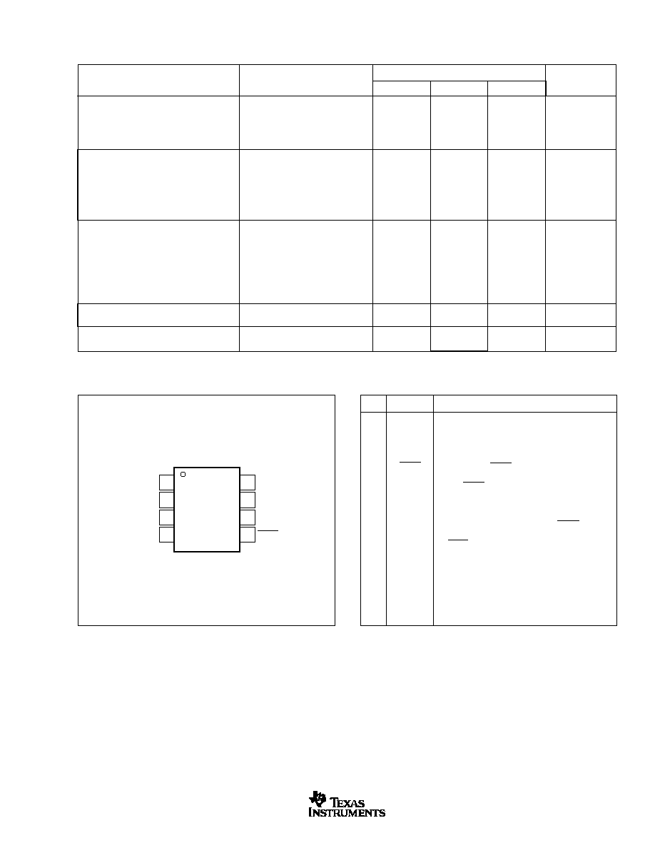
PIN
NAME
DESCRIPTION
1
V
DD
Power supply input, +2.7V to +5.5V.
2
V
REF
Reference voltage input.
3
V
OUT
B
Analog output voltage from DAC B.
4
V
OUT
A
Analog output voltage from DAC A.
5
SYNC
Level triggered SYNC input (active LOW). This is the
frame synchronization signal for the input data.
When SYNC goes LOW, it enables the input shift
register and data is transferred on the falling edge of
SCLK. The action specified by the 8-bit control byte
and 16-bit data word is executed following the 24th
falling SCLK clock edge (unless SYNC is taken
HIGH before this edge in which case the rising edge
of SYNC acts as an interrupt and the write sequence
is ignored by the DAC8532).
6
SCLK
Serial Clock Input. Data can be transferred at rates
up to 30 MHz at 5V.
7
D
IN
Serial Data Input. Data is clocked into the 24-bit
input shift register on each falling edge of the serial
clock input.
8
GND
Ground reference point for all circuitry on the part.
PIN DESCRIPTIONS
PIN CONFIGURATION
Top View
MSOP-8
V
DD
V
REF
V
OUT
B
V
OUT
A
GND
D
IN
SCLK
SYNC
1
2
3
4
8
7
6
5
DAC8532
DAC8532
4
SBAS246A
www.ti.com
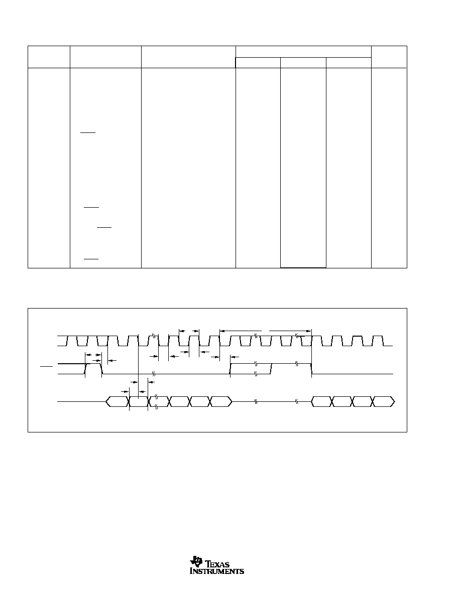
SERIAL WRITE OPERATION
SCLK
1
24
SYNC
D
IN
DB23
DB0
DB23
t
8
t
3
t
2
t
7
t
4
t
5
t
6
t
1
t
9
PARAMETER
DESCRIPTION
CONDITIONS
MIN
TYP
MAX
UNITS
t
1
(3)
SCLK Cycle Time
V
DD
= 2.7V to 3.6V
50
ns
V
DD
= 3.6V to 5.5V
33
ns
t
2
SCLK HIGH Time
V
DD
= 2.7V to 3.6V
13
ns
V
DD
= 3.6V to 5.5V
13
ns
t
3
SCLK LOW Time
V
DD
= 2.7V to 3.6V
22.5
ns
V
DD
= 3.6V to 5.5V
13
ns
t
4
SYNC to SCLK Rising
Edge Setup Time
V
DD
= 2.7V to 3.6V
0
ns
V
DD
= 3.6V to 5.5V
0
ns
t
5
Data Setup Time
V
DD
= 2.7V to 3.6V
5
ns
V
DD
= 3.6V to 5.5V
5
ns
t
6
Data Hold Time
V
DD
= 2.7V to 3.6V
4.5
ns
V
DD
= 3.6V to 5.5V
4.5
ns
t
7
24th SCLK Falling Edge to
SYNC Rising Edge
V
DD
= 2.7V to 3.6V
0
ns
V
DD
= 3.6V to 5.5V
0
ns
t
8
Minimum SYNC HIGH Time
V
DD
= 2.7V to 3.6V
50
ns
V
DD
= 3.6V to 5.5V
33
ns
t
9
24th SCLK Falling Edge to
SYNC Falling Edge
V
DD
= 2.7V to 5.5V
100
ns
NOTES: (1) All input signals are specified with t
R
= t
F
= 5ns (10% to 90% of V
DD
) and timed from a voltage level of (V
IL
+ V
IH
)/2. (2) See Serial Write Operation timing
diagram, below. (3) Maximum SCLK frequency is 30MHz at V
DD
= +3.6V to +5.5V and 20MHz at V
DD
= +2.7V to +3.6V.
TIMING CHARACTERISTICS
(1, 2)
V
DD
= +2.7V to +5.5V; all specifications �40
�
C to +105
�
C unless otherwise noted.
DAC8532
5
DAC8532
SBAS246A
www.ti.com
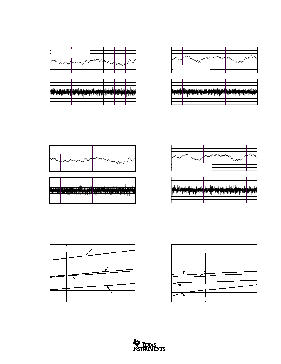
TYPICAL CHARACTERISTICS
At T
A
= +25
�
C, unless otherwise noted.
64
48
32
16
0
�16
�32
�48
�64
LE (LSB)
LINEARITY ERROR AND
DIFFERENTIAL LINEARITY ERROR vs CODE
0000
H
2000
H
4000
H
6000
H
8000
H
Digital Input Code
A000
H
C000
H
E000
H
FFFF
H
2.0
1.5
1.0
0.5
0.0
�0.5
�1.0
�1.5
�2.0
DLE (LSB)
V
DD
= V
REF
= 5V, T
A
= 25
�
C,
Channel A Output
64
48
32
16
0
�16
�32
�48
�64
LE (LSB)
LINEARITY ERROR AND
DIFFERENTIAL LINEARITY ERROR vs CODE
0000
H
2000
H
4000
H
6000
H
8000
H
Digital Input Code
A000
H
C000
H
E000
H
FFFF
H
2.0
1.5
1.0
0.5
0.0
�0.5
�1.0
�1.5
�2.0
DLE (LSB)
V
DD
= V
REF
= 5V, T
A
= 25
�
C,
Channel B Output
64
48
32
16
0
�16
�32
�48
�64
LE (LSB)
LINEARITY ERROR AND
DIFFERENTIAL LINEARITY ERROR vs CODE
0000
H
2000
H
4000
H
6000
H
8000
H
Digital Input Code
A000
H
C000
H
E000
H
FFFF
H
2.0
1.5
1.0
0.5
0.0
�0.5
�1.0
�1.5
�2.0
DLE (LSB)
V
DD
= V
REF
= 2.7V, T
A
= 25
�
C,
Channel A Output
64
48
32
16
0
�16
�32
�48
�64
LE (LSB)
LINEARITY ERROR AND
DIFFERENTIAL LINEARITY ERROR vs CODE
0000
H
2000
H
4000
H
6000
H
8000
H
Digital Input Code
A000
H
C000
H
E000
H
FFFF
H
2.0
1.5
1.0
0.5
0.0
�0.5
�1.0
�1.5
�2.0
DLE (LSB)
V
DD
= V
REF
= 2.7V, T
A
= 25
�
C,
Channel B Output
ZERO-SCALE ERROR vs TEMPERATURE
�40
Output Error (mV)
Temperature (
�
C)
�10
20
50
80
105
25
20
15
10
5
0
V
DD
= V
REF
V
DD
= 5V, CH B
V
DD
= 5V, CH A
V
DD
= 2.7V, CH A
V
DD
= 2.7V, CH B
FULL-SCALE ERROR vs TEMPERATURE
�40
Output Error (mV)
Temperature (
�
C)
�10
20
50
80
105
15
10
5
0
�5
�10
�15
(To avoid clipping of the output signal
during the test, V
REF
= V
DD
� 10mV)
V
DD
= 5V, CH A
V
DD
= 2.7V, CH A
V
DD
= 2.7V, CH B
V
DD
= 5V, CH B
DAC8532
6
SBAS246A
www.ti.com
TYPICAL CHARACTERISTICS
(Cont.)
At T
A
= +25
�
C, unless otherwise noted.
ABSOLUTE ERROR
0000
H
2000
H
4000
H
6000
H
8000
H
Digital Input Code
A000
H
C000
H
E000
H
FFFF
H
30
25
20
15
10
5
0
�5
�10
�15
�20
�25
�30
Output Error (mV)
V
DD
= V
REF
= 5V, T
A
= 25
�
C
Channel A Output
Channel B Output
ABSOLUTE ERROR
0000
H
2000
H
4000
H
6000
H
8000
H
Digital Input Code
A000
H
C000
H
E000
H
FFFF
H
30
25
20
15
10
5
0
�5
�10
�15
�20
�25
�30
Output Error (mV)
V
DD
= V
REF
= 2.7V, T
A
= 25
�
C
Channel A Output
Channel B Output
HISTOGRAM OF CURRENT CONSUMPTION
Frequency
I
DD
(
�
A)
2500
2000
1500
1000
500
0
400
440
480
520
560
600
640
680
720
760
800
V
DD
= V
REF
= 5V
,
Reference Current Included
HISTOGRAM OF CURRENT CONSUMPTION
Frequency
I
DD
(
�
A)
2500
2000
1500
1000
500
0
280
320
360
400
440
480
520
560
600
640
680
V
DD
= V
REF
= 2.7V
,
Reference Current Included
SINK CURRENT CAPABILITY
0
V
OUT
(V)
I
SINK
(mA)
1
2
3
4
5
0.15
0.125
0.1
0.075
0.05
0.025
0
V
REF
= V
DD
� 10mV
DAC Loaded with 0000
H
V
DD
= 2.7V
V
DD
= 5V
OUTPUT VOLTAGE DRIFT
Time (1min/div)
V
OUT
(25
�
V/div)
V
DD
= V
REF
= 5V, T
A
= 25
�
C (
�
1
�
C),
Digital Code = 7FFF
H
7
DAC8532
SBAS246A
www.ti.com
TYPICAL CHARACTERISTICS
(Cont.)
At T
A
= +25
�
C, unless otherwise noted.
SOURCE CURRENT CAPABILITY
0
V
OUT
(V)
I
SOURCE
(mA)
1
2
3
4
5
5
4.95
4.9
4.85
4.8
V
REF
= V
DD
� 10mV
DAC Loaded with FFFF
H
V
DD
= 5V
SOURCE CURRENT CAPABILITY
0
V
OUT
(V)
I
SOURCE
(mA)
1
2
3
4
5
2.7
2.65
2.6
2.55
2.5
V
REF
= V
DD
� 10mV
DAC Loaded with FFFF
H
V
DD
= 2.7V
SUPPLY CURRENT vs TEMPERATURE
700
600
500
400
300
200
100
0
I
DD
(
�
A)
�40
Temperature (
�
C)
�10
20
50
80
105
V
DD
= V
REF
= 5V
V
DD
= V
REF
= 2.7V
Reference Current Included,
CH A and CH B Active, No Load
SUPPLY CURRENT vs DIGITAL INPUT CODE
0000
H
2000
H
4000
H
6000
H
8000
H
Digital Input Code
A000
H
C000
H
E000
H
FFFF
H
700
600
500
400
300
200
100
0
I
DD
(
�
A)
V
DD
= V
REF
= 5V
V
DD
= V
REF
= 2.7V
POWER-DOWN CURRENT vs SUPPLY VOLTAGE
50
45
40
35
30
25
20
15
10
5
0
I
DD
(nA)
2.7
V
DD
(V)
3.4
4.1
4.8
5.5
Reference Current Excluded
T
A
= +105
�
C
T
A
= �40
�
C
T
A
= +25
�
C
SUPPLY CURRENT vs SUPPLY VOLTAGE
800
750
700
650
600
550
500
450
400
I
DD
(
�
A)
2.7
V
DD
(V)
3.05
3.75
3.4
4.45
4.1
5.15
4.8
5.5
V
REF
= V
DD
, Both DACs Active,
Reference Current Included, No Load
DAC8532
8
SBAS246A
www.ti.com
TYPICAL CHARACTERISTICS
(Cont.)
At T
A
= +25
�
C, unless otherwise noted.
SUPPLY CURRENT vs LOGIC INPUT VOLTAGE
0
I
DD
(
�
A)
V
LOGIC
(V)
1
2
3
4
5
1150
1050
950
850
750
650
550
450
V
DD
= V
REF
= 5V
V
DD
= V
REF
= 2.7V
T
A
= 25
�
C, SYNC Input (All Other Inputs = GND)
Reference Current Included,
CHA and CHB Active,
No Load
FULL-SCALE SETTLING TIME
(Large Signal)
Time (2
�
s/div)
5
4
3
2
1
0
V
OUT
(V)
V
DD
= V
REF
= 5V,
Output Loaded with
2k
and 200pF to
GND
HALF-SCALE SETTLING TIME
(Large Signal)
Time (2
�
s/div)
3
2.5
2
1.5
1
0.5
0
V
OUT
(V)
V
DD
= V
REF
= 5V,
Output Loaded with
2k
and 200pF
to GND.
FULL-SCALE SETTLING TIME
(Large Signal)
Time (2
�
s/div)
3.5
3
2.5
2
1.5
1
0.5
0
V
OUT
(V)
V
DD
= V
REF
= 2.7V,
Output Loaded with
2k
and 200pF
to GND.
HALF-SCALE SETTLING TIME
(Large Signal)
Time (2
�
s/div)
1.5
1
0.5
0
V
OUT
(V)
V
DD
= V
REF
= 2.7V,
Output Loaded with
2k
and 200pF
to GND.
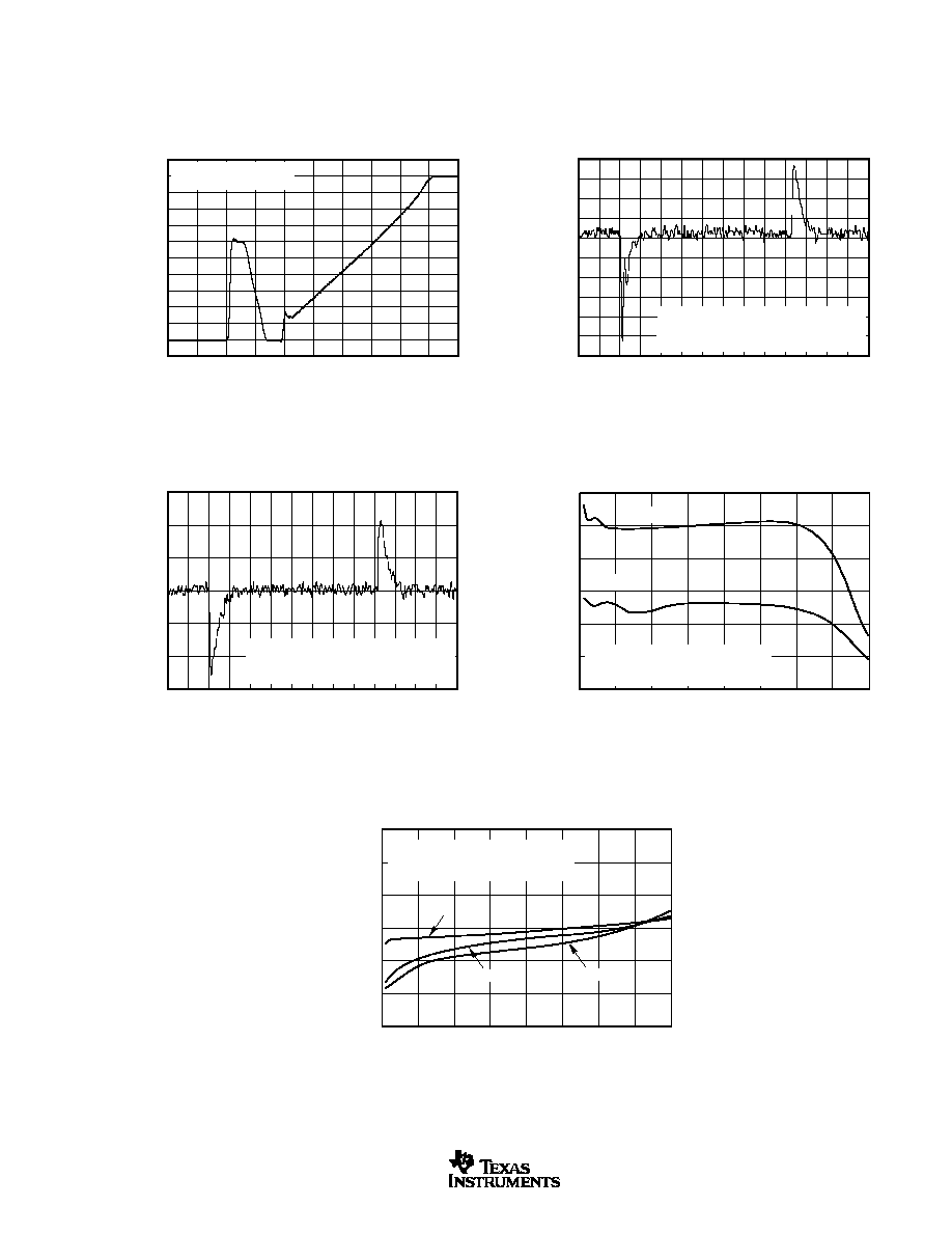
POWER-ON RESET TO ZERO-SCALE
Time (100
�
s/div)
Loaded with 2k
to GND
V
DD
(2V/div)
V
OUT
(1V/div)
9
DAC8532
SBAS246A
www.ti.com
TYPICAL CHARACTERISTICS
(Cont.)
At T
A
= +25
�
C, unless otherwise noted.
EXITING POWER-DOWN MODE
Time (1
�
s/div)
5.5
5
4.5
4
3.5
3
2.5
2
1.5
1
0.5
0
�0.5
V
OUT
(V)
V
DD
= V
REF
= 5V
Power Up to Code FFFF
H
OUTPUT GLITCH
(Mid-Scale)
Time (1
�
s/div)
2.54
2.52
2.5
2.48
2.46
2.44
2.42
V
OUT
(V, 20mV/div)
V
DD
= V
REF
= 5V
Code 8000
H
to 7FFF
H
to 8000
H
(Glitch Occurs Every N � 4096 Code Boundary)
SIGNAL-TO-NOISE RATIO vs OUTPUT FREQUENCY
96
94
92
90
88
86
84
SNR (dB)
0
Output Frequency (Hz)
500
1500
1000
2500
2000
3500
3000
4000
V
DD
= V
REF
�1dB FSR Digital Input, F
S
= 52ksps
Measurement Bandwidth = 20kHz
V
DD
= 5V
V
DD
= 2.7V
TOTAL HARMONIC DISTORTION
vs OUTPUT FREQUENCY
0
�20
�40
�60
�80
�100
�120
THD (dB)
0
Output Frequency (Hz)
500
1500
1000
2500
2000
3500
3000
4000
V
DD
= V
REF
= 5V
�1dB FSR Digital Input, F
S
= 52ksps
Measurement Bandwidth = 20kHz
2nd Harmonic
THD
3rd Harmonic
OUTPUT GLITCH
(Worst Case)
Time (1
�
s/div)
4.72
4.7
4.68
4.66
4.64
4.62
4.6
4.58
4.56
4.54
4.52
V
OUT
(V, 20mV/div)
V
DD
= V
REF
= 5V
Code F000
H
to EFFF
H
to F000
H
(Glitch Occurs Every N � 4096 Code Boundary)
DAC8532
10
SBAS246A
www.ti.com
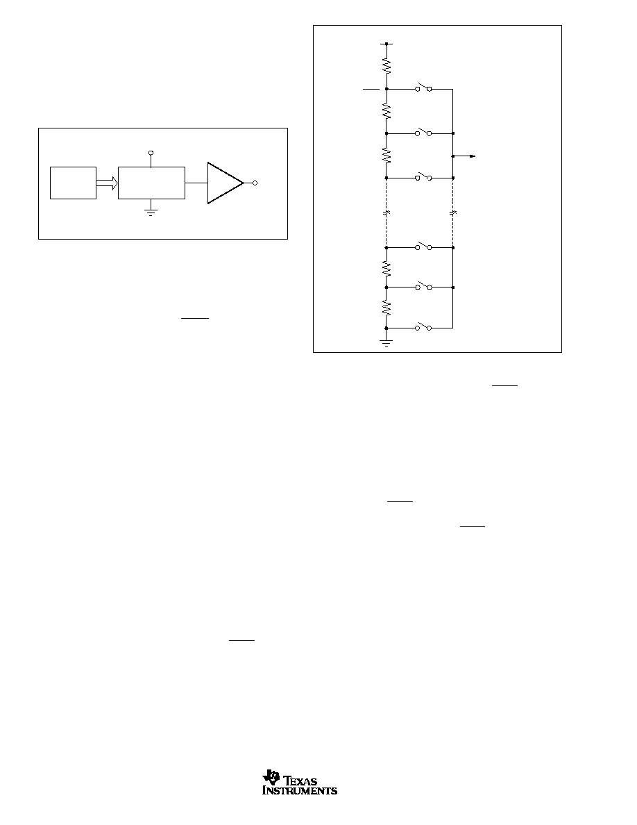
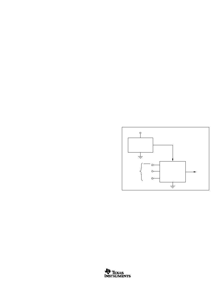
THEORY OF OPERATION
DAC SECTION
The architecture of each channel of the DAC8532 consists of
a resistor string DAC followed by an output buffer amplifier.
Figure 1 shows a simplified block diagram of the DAC
architecture.
The input coding for each device is unipolar straight binary,
so the ideal output voltage is given by:
V
X
V
D
OUT
REF
=
�
65536
where D = decimal equivalent of the binary code that is
loaded to the DAC register; it can range from 0 to 65535.
V
OUT
X refers to channel A or B.
RESISTOR STRING
The resistor string section is shown in Figure 2. It is simply
a divide-by-2 resistor followed by a string of resistors, each
of value R. The code loaded into the DAC register deter-
mines at which node on the string the voltage is tapped off.
This voltage is then applied to the output amplifier by closing
one of the switches connecting the string to the amplifier.
OUTPUT AMPLIFIER
Each output buffer amplifier is capable of generating rail-to-
rail voltages on its output which approaches an output range
of 0V to V
DD
(gain and offset errors must be taken into
account). Each buffer is capable of driving a load of 2k
in
parallel with 1000pF to GND. The source and sink capabili-
ties of the output amplifier can be seen in the typical charac-
teristics.
SERIAL INTERFACE
The DAC8532 uses a 3-wire serial interface (SYNC, SCLK,
and D
IN
), which is compatible with SPITM, QSPITM, and
MicrowireTM interface standards, as well as most DSPs. See
the Serial Write Operation timing diagram for an example of
a typical write sequence.
SPI and QSP are registered trademarks of Motorola.
Microwire is a registered trademark of National Semiconductor.
DAC Register
REF (+)
Resistor String
REF(�)
Output
Amplifier
GND
V
REF
V
OUT
X
FIGURE 1. DAC8532 Architecture.
To Output
Amplifier
(2x Gain)
R
R
R
R
V
REF
2
V
REF
R
DIVIDER
FIGURE 2. Resistor String.
The write sequence begins by bringing the SYNC line LOW.
Data from the D
IN
line is clocked into the 24-bit shift register
on each falling edge of SCLK. The serial clock frequency can
be as high as 30MHz, making the DAC8532 compatible with
high speed DSPs. On the 24th falling edge of the serial clock,
the last data bit is clocked into the shift register and the
programmed function is executed (i.e., a change in Data
Buffer contents, DAC Register contents, and/or a change in
the power-down mode of a specified channel or channels).
At this point, the SYNC line may be kept LOW or brought
HIGH. In either case, the minimum delay time from the 24th
falling SCLK edge to the next falling SYNC edge must be met
in order to properly begin the next cycle. To assure the
lowest power consumption of the device, care should be
taken that the digital input levels are as close to each rail as
possible. (Please refer to the "Typical Characteristics" sec-
tion for the "Supply Current vs Logic Input Voltage" transfer
characteristic curve).

11
DAC8532
SBAS246A
www.ti.com
INPUT SHIFT REGISTER
The input shift register of the DAC8532 is 24 bits wide (see
Figure 5) and is made up of 8 control bits (DB16-DB23) and 16
data bits (DB0-DB15). The first two control bits (DB22 and
DB23) are reserved and must be "0" for proper operation. LD
A (DB20) and LD B (DB21) control the updating of each analog
output with the specified 16-bit data value or power-down
command. Bit DB19 is a "Don't Care" bit which does not affect
the operation of the DAC8532 and can be 1 or 0. The following
control bit, Buffer Select (DB18), controls the destination of the
data (or power-down command) between DAC A and DAC B.
The final two control bits, PD0 (DB16) and PD1 (DB17), select
the power-down mode of one or both of the DAC channels. The
four modes are normal mode or any one of three power-down
modes. A more complete description of the operational modes
of the DAC8532 can be found in the Power-Down Modes
section. The remaining sixteen bits of the 24-bit input word
make up the data bits. These are transferred to the specified
Data Buffer or DAC Register, depending on the command
issued by the control byte, on the 24th falling edge of SCLK.
Please refer to Tables II and III for more information.
are set to zero-scale; they remain there until a valid write
sequence and load command is made to the respective
DAC channel. This is useful in applications where it is
important to know the state of the output of each DAC
output while the device is in the process of powering up.
No device pin should be brought high before power is
applied to the device.
POWER-DOWN MODES
The DAC8532 utilizes four modes of operation. These modes
are accessed by setting two bits (PD1 and PD0) in the control
register and performing a "Load" action to one or both DACs.
Table I shows how the state of the bits correspond to the
mode of operation of each channel of the device. (Each DAC
channel can be powered down simultaneously or indepen-
dently of each other. Power-down occurs after proper data is
written into PD0 and PD1 and a "Load" command occurs.)
Please refer to the "Operation Examples" section for addi-
tional information.
Resistor
String DAC
Amplifier
Power-down
Circuitry
Resistor
Network
V
OUT
X
FIGURE 3. Output Stage During Power-Down (High-Impedance)
SYNC INTERRUPT
In a normal write sequence, the SYNC line is kept LOW for
at least 24 falling edges of SCLK and the addressed DAC
register is updated on the 24th falling edge. However, if
SYNC is brought HIGH before the 24th falling edge, it acts as
an interrupt to the write sequence; the shift register is reset
and the write sequence is discarded. Neither an update of
the data buffer contents, DAC register contents or a change
in the operating mode occurs (see Figure 4).
POWER-ON RESET
The DAC8532 contains a power-on reset circuit that con-
trols the output voltage during power-up. On power-up, the
DAC registers are filled with zeros and the output voltages
PD1 (DB17)
PD0 (DB16)
OPERATING MODE
0
0
Normal Operation
--
--
Power-Down Modes
0
1
Output Typically 1k
to GND
1
0
Output Typically 100k
to GND
1
1
High Impedance
TABLE I. Modes of Operation for the DAC8532.
When both bits are set to 0, the device works normally with
a typical power consumption of 500
�
A at 5V. For the three
power-down modes, however, the supply current falls to
200nA at 5V (50nA at 3V). Not only does the supply current
fall but the output stage is also internally switched from the
output of the amplifier to a resistor network of known values.
This has the advantage that the output impedance of the
device is known while it is in power-down mode. There are
three different options for power-down: The output is con-
nected internally to GND through a 1k
resistor, a 100k
resistor, or it is left open-circuited (High-Impedance). The
output stage is illustrated in Figure 3.
All analog circuitry is shut down when the power-down mode
is activated. Each DAC will exit power-down when PD0 and
PD1 are set to 0, new data is written to the Data Buffer, and
the DAC channel receives a "Load" command. The time to
exit power-down is typically 2.5
�
s for V
DD
= 5V and 5
�
s for
V
DD
= 3V (See the Typical Characteristics).

DAC8532
12
SBAS246A
www.ti.com
D17
D16
PD1
PD0
0
1
1k
1
0
100k
1
1
High Impedance
TABLE III. Power-Down Commands.
OUTPUT IMPEDANCE POWERDOWN COMMANDS
0
0
LDB
LDA
X
Buffer Select
PD1
PD0
D15
D14
D13
D12
D11
D10
D9
D8
D7
D6
D5
D4
D3
D2
D1
D0
DB11
DB0
FIGURE 5. DAC8532 Data Input Register Format.
DB23
DB12
D23
D22
D21
D20
D19
D18
D17
D16
Reserved Reserved Load B Load A Don't Care Buffer Select
PD1
PD0
0 = A, 1 = B
0
0
0
0
X
#
0
0
Data
WR Buffer # w/Data
0
0
0
0
X
#
X
WR Buffer # w/Power-Down Command
0
0
0
1
X
#
0
0
Data
WR Buffer # w/Data and Load DAC A
0
0
0
1
X
0
X
WR Buffer A w/Power-Down Command and LOAD DAC A
(DAC A Powered Down)
0
0
0
1
X
1
X
WR Buffer B w/ Power-Down Command and LOAD DAC A
0
0
1
0
X
#
0
0
Data
WR Buffer # w/Data and Load DAC B
0
0
1
0
X
0
X
WR Buffer A w/Power-Down Command and LOAD DAC B
0
0
1
0
X
1
X
WR Buffer B w/ Power-Down Command and LOAD DAC B
(DAC B Powered Down)
0
0
1
1
X
#
0
0
Data
WR Buffer # w/Data and Load DACs A and B
0
0
1
1
X
0
X
WR Buffer A w/Power-Down Command and Load DACs A
and B (DAC A Powered Down)
0
0
1
1
X
1
X
WR Buffer B w/Power-Down Command and Load DACs A
and B (DAC B Powered Down)
D15
D14
D13-D0
MSB
MSB-1
MSB-2...LSB
(see Table III)
(see Table III)
(see Table III)
(Always Write 0)
TABLE II. Control Matrix.
DESCRIPTION
(see Table III)
(see Table III)
(see Table III)
(see Table III)
SCLK
SYNC
DIN
Invalid Write-Sync Interrupt:
SYNC HIGH before 24th Falling Edge
Valid Write -Buffer/DAC Update:
SYNC HIGH after 24th Falling Edge
DB23 DB22
1
2
1
2
DB0
DB23 DB22
DB1
DB0
24th Falling
Edge
24th Falling
Edge
FIGURE 4. Interrupt and Valid SYNC Timing.
13
DAC8532
SBAS246A
www.ti.com
OPERATION EXAMPLES
Example 1: Write to Data Buffer A; Write to Data Buffer B; Load DACA and DACB Simultaneously
�
1st--Write to Data Buffer A:
�
2nd--Write to Data Buffer B and Load DAC A and DAC B simultaneously:
Reserved
Reserved
LDB
LDA
DC
Buffer Select
PD1
PD0
DB15
......
DB1
DB0
0
0
0
0
X
0
0
0
D15
.....
D1
D0
The DACA and DACB analog outputs simultaneously settle to the specified values upon completion of the 2
nd
write sequence.
(The "Load" command moves the digital data from the data buffer to the DAC register at which time the conversion takes place
and the analog output is updated. "Completion" occurs on the 24
th
falling SCLK edge after SYNC LOW.)
Example 2: Load New Data to DACA and DACB Sequentially
�
1st--Write to Data Buffer A and Load DAC A: DACA output settles to specified value on completion:
Reserved
Reserved
LDB
LDA
DC
Buffer Select
PD1
PD0
DB15
......
DB1
DB0
0
0
1
1
X
1
0
0
D15
.....
D1
D0
�
2nd--Write to Data Buffer B and Load DAC B: DACB output settles to specified value on completion:
Reserved
Reserved
LDB
LDA
DC
Buffer Select
PD1
PD0
DB15
......
DB1
DB0
0
0
0
1
X
0
0
0
D15
.....
D1
D0
After completion of the 1
st
write cycle, the DACA analog output settles to the voltage specified; upon completion of write cycle 2,
the DACB analog output settles.
Example 3: Power-Down DACA to 1k
and Power-Down DACB to 100k
Simultaneously
�
1st--Write power-down command to Data Buffer A:
Reserved
Reserved
LDB
LDA
DC
Buffer Select
PD1
PD0
DB15
......
DB1
DB0
0
0
1
0
X
1
0
0
D15
.....
D1
D0
�
2nd--Write power-down command to Data Buffer B and Load DACA and DACB simultaneously:
Reserved
Reserved
LDB
LDA
DC
Buffer Select
PD1
PD0
DB15
......
DB1
DB0
0
0
0
0
X
0
0
1
Don't Care
Reserved
Reserved
LDB
LDA
DC
Buffer Select
PD1
PD0
DB15
......
DB1
DB0
0
0
1
1
X
1
1
0
Don't Care
The DACA and DACB analog outputs simultaneously power-down to each respective specified mode upon completion of the
2
nd
write sequence.
Example 4: Power-Down DACA and DACB to High Impedance Sequentially:
�
1st--Write power-down command to Data Buffer A and Load DAC A: DAC A output = High-Z:
Reserved
Reserved
LDB
LDA
DC
Buffer Select
PD1
PD0
DB15
......
DB1
DB0
0
0
0
1
X
0
1
1
Don't Care
Reserved
Reserved
LDB
LDA
DC
Buffer Select
PD1
PD0
DB15
......
DB1
DB0
0
0
1
0
X
1
1
1
Don't Care
�
2nd--Write power-down command to Data Buffer B and Load DAC B: DAC B output = High-Z:
The DACA and DACB analog outputs sequentially power-down to high impedance upon completion of the 1
st
and 2
nd
write
sequences, respectively.
DAC8532
14
SBAS246A
www.ti.com
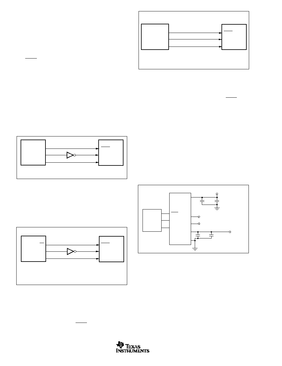
DAC8532 to Microwire INTERFACE
Figure 7 shows an interface between the DAC8532 and any
Microwire compatible device. Serial data is shifted out on the
falling edge of the serial clock and is clocked into the
DAC8532 on the rising edge of the SK signal.
MICROPROCESSOR
INTERFACING
DAC8532 to 8051 INTERFACE
Figure 6 shows a serial interface between the DAC8532 and
a typical 8051-type microcontroller. The setup for the inter-
face is as follows: TXD of the 8051 drives SCLK of the
DAC8532, while RXD drives the serial data line of the device.
The SYNC signal is derived from a bit-programmable pin on
the port of the 8051. In this case, port line P3.3 is used. When
data is to be transmitted to the DAC8532, P3.3 is taken LOW.
The 8051 transmits data in 8-bit bytes; thus only eight falling
clock edges occur in the transmit cycle. To load data to the
DAC, P3.3 is left LOW after the first eight bits are transmitted,
then a second and third write cycle is initiated to transmit the
remaining data. P3.3 is taken HIGH following the completion
of the third write cycle. The 8051 outputs the serial data in a
format which presents the LSB first, while the DAC8532
requires its data with the MSB as the first bit received. The
8051 transmit routine must therefore take this into account,
and "mirror" the data as needed.
The 68HC11 should be configured so that its CPOL bit is 0
and its CPHA bit is 1. This configuration causes data appear-
ing on the MOSI output to be valid on the falling edge of SCK.
When data is being transmitted to the DAC, the SYNC line is
held LOW (PC7). Serial data from the 68HC11 is transmitted
in 8-bit bytes with only eight falling clock edges occurring in
the transmit cycle. (Data is transmitted MSB first.) In order to
load data to the DAC8532, PC7 is left LOW after the first
eight bits are transferred, then a second and third serial write
operation is performed to the DAC. PC7 is taken HIGH at the
end of this procedure.
DAC8532 to TMS320 DSP INTERFACE
Figure 9 shows the connections between the DAC8532 and
a TMS320 digital signal processor. By decoding the FSX
signal, multiple DAC8532s can be connected to a single
serial port of the DSP.
FIGURE 6. DAC8532 to 80C51/80L51 Interface.
FIGURE 7. DAC8532 to Microwire Interface.
FIGURE 8. DAC8532 to 68HC11 Interface.
DAC8532 to 68HC11 INTERFACE
Figure 8 shows a serial interface between the DAC8532 and
the 68HC11 microcontroller. SCK of the 68HC11 drives the
SCLK of the DAC8532, while the MOSI output drives the
serial data line of the DAC. The SYNC signal is derived from
a port line (PC7), similar to the 8051 diagram.
FIGURE 9. DAC8532 to TMS320 DSP.
DAC8532
TMS320 DSP
SYNC
D
IN
SCLK
FSX
DX
CLKX
V
DD
V
OUT
A
V
OUT
B
Output A
Output B
Reference
Input
V
REF
GND
0.1
�
F
1
�
F to 10
�
F
Positive Supply
0.1
�
F
10
�
F
APPLICATIONS
CURRENT CONSUMPTION
The DAC8532 typically consumes 250uA at V
DD
= 5V and
225uA at V
DD
= 3V for each active channel, including refer-
ence current consumption. Additional current consumption
can occur at the digital inputs if V
IH
<<V
DD
. For most efficient
power operation, CMOS logic levels are recommended at the
digital inputs to the DAC.
In power-down mode, typical current consumption is 200nA.
A delay time of 10 to 20ms after a power-down command is
issued to the DAC is typically sufficient for the power-down
current to drop below 10
�
A.
80C51/80L51
(1)
P3.3
TXD
RXD
DAC8532
(1)
SYNC
SCLK
D
IN
NOTE: (1) Additional pins omitted for clarity.
SYNC
SCLK
D
IN
Microwire
TM
CS
SK
SO
DAC8532
(1)
NOTE: (1) Additional pins omitted for clarity.
Microwire is a registered trademark of National Semiconductor.
68HC11
(1)
PC7
SCK
MOSI
SYNC
SCLK
D
IN
DAC8532
(1)
NOTE: (1) Additional pins omitted for clarity.
15
DAC8532
SBAS246A
www.ti.com
DRIVING RESISTIVE AND CAPACITIVE LOADS
The DAC8532 output stage is capable of driving loads of up
to 1000pF while remaining stable. Within the offset and gain
error margins, the DAC8532 can operate rail-to-rail when
driving a capacitive load. Resistive loads of 2k
can be
driven by the DAC8532 while achieving a typical load regu-
lation of 1%. As the load resistance drops below 2k
, the
load regulation error increases. When the outputs of the DAC
are driven to the positive rail under resistive loading, the
PMOS transistor of each Class-AB output stage can enter
into the linear region. When this occurs, the added IR voltage
drop deteriorates the linearity performance of the DAC. This
only occurs within approximately the top 20mV of the DAC's
digital input-to-voltage output transfer characteristic. The
reference voltage applied to the DAC8532 may be reduced
below the supply voltage applied to V
DD
in order to eliminate
this condition if good linearity is a requirement at full scale
(under resistive loading conditions).
CROSSTALK AND AC PERFORMANCE
The DAC8532 architecture uses separate resistor strings for
each DAC channel in order to achieve ultra-low crosstalk
performance. DC crosstalk seen at one channel during a full-
scale change on the neighboring channel is typically less than
0.5LSBs. The AC crosstalk measured (for a full-scale, 1kHz
sine wave output generated at one channel, and measured at
the remaining output channel) is typically under �100dB.
In addition, the DAC8532 can achieve typical AC perfor-
mance of 96dB SNR (Signal-to-Noise Ratio) and 65db THD
(Total Harmonic Distortion), making the DAC8532 a solid
choice for applications requiring low SNR at output frequen-
cies at or below 4kHz.
OUTPUT VOLTAGE STABILITY
The DAC8532 exhibits excellent temperature stability of
5ppm/
�
C typical output voltage drift over the specified tem-
perature range of the device. This enables the output voltage
of each channel to stay within a
�
25
�
V window for a
�
1
�
C
ambient temperature change.
Good Power-Supply Rejection Ratio (PSRR) performance
reduces supply noise present on V
DD
from appearing at the
outputs to well below 10
�
V-s. Combined with good DC noise
performance and true 16-bit differential linearity, the DAC8532
becomes a perfect choice for closed-loop control applica-
tions.
SETTLING TIME AND OUTPUT
GLITCH PERFORMANCE
Settling time to within the 16-bit accurate range of the
DAC8532 is achievable within 10
�
s for a full-scale code
change at the input. Worst case settling times between
consecutive code changes is typically less than 2
�
s, en-
abling update rates up to 500ksps for digital input signals
changing code-to-code. The high-speed serial interface of
the DAC8532 is designed in order to support these high
update rates.
For full-scale output swings, the output stage of each
DAC8532 channel typically exhibits less than 100mV of
overshoot and undershoot when driving a 200pF capacitive
load. Code-to-code change glitches are extremely low
(~10uV) given that the code-to-code transition does not
cross an Nx4096 code boundary. Due to internal segmen-
tation of the DAC8532, code-to-code glitches occur at each
crossing of an Nx4096 code boundary. These glitches can
approach 100mVs for N = 15, but settle out within ~2
�
s.
USING REF02 AS A POWER SUPPLY FOR DAC8532
Due to the extremely low supply current required by the
DAC8532, a possible configuration is to use a REF02 +5V
precision voltage reference to supply the required voltage to
the DAC8532's supply input as well as the reference input, as
shown in Figure 10. This is especially useful if the power
supply is quite noisy or if the system supply voltages are at
some value other than 5V. The REF02 will output a steady
supply voltage for the DAC8532. If the REF02 is used, the
current it needs to supply to the DAC8532 is 567
�
A typical
and 890
�
A max for V
DD
= 5V. When a DAC output is loaded,
the REF02 also needs to supply the current to the load. The
total typical current required (with a 5k
load on a given DAC
output) is:
567
�
A + (5V/ 5k
) = 1.567mA
FIGURE 10. REF02 as a Power Supply to the DAC8532.
REF02
DAC8532
3-Wire
Serial
Interface
+5V
1.567mA
V
DD
, V
REF
V
OUT
= 0V to 5V
SYNC
SCLK
D
IN
+15
The load regulation of the REF02 is typically 0.005%/mA,
which results in an error of 392
�
V for the 1.5mA current
drawn from it. This corresponds to a 5.13LSB error for a 0V
to 5V output range.
BIPOLAR OPERATION USING THE DAC8532
The DAC8532 has been designed for single-supply opera-
tion but a bipolar output range is also possible using the
circuit in Figure 11. The circuit shown will give an output
voltage range of
�
V
REF
. Rail-to-rail operation at the amplifier
output is achievable using an amplifier such as the OPA703,
see Figure 11.
DAC8532
16
SBAS246A
www.ti.com
The output voltage for any input code can be calculated as
follows:
V
X
V
D
R
R
R
V
R
R
OUT
REF
REF
=
�
�
+
�
65536
1
2
1
2
1
�
where D represents the input code in decimal (0�65535).
With V
REF
= 5V, R
1
= R
2
= 10k
:
V
X
D
V
OUT
=
�
10
65536
5
�
This is an output voltage range of
�
5V with 0000
H
corre-
sponding to a �5V output and FFFF
H
corresponding to a +5V
output. Similarly, using V
REF
= 2.5V, a
�
2.5V output voltage
range can be achieved.
LAYOUT
A precision analog component requires careful layout, ad-
equate bypassing, and clean, well-regulated power supplies.
The DAC8532 offers single-supply operation, and it will often
be used in close proximity with digital logic, microcontrollers,
microprocessors, and digital signal processors. The more
digital logic present in the design and the higher the switch-
ing speed, the more difficult it will be to keep digital noise
from appearing at the output.
FIGURE 11. Bipolar Operation with the DAC8532.
DAC8532
(Other pins omitted for clarity.)
V
DD
, V
REF
V
OUT
X
R
1
10k
R
2
10k
+5V
10
�
F
0.1
�
F
�5V
�
5V
+5V
OPA703
Due to the single ground pin of the DAC8532, all return
currents, including digital and analog return currents for the
DAC, must flow through a single point. Ideally, GND would
be connected directly to an analog ground plane. This plane
would be separate from the ground connection for the digital
components until they were connected at the power entry
point of the system.
The power applied to V
DD
should be well regulated and low
noise. Switching power supplies and DC/DC converters will
often have high-frequency glitches or spikes riding on the
output voltage. In addition, digital components can create
similar high-frequency spikes as their internal logic switches
states. This noise can easily couple into the DAC output
voltage through various paths between the power connec-
tions and analog output.
As with the GND connection, V
DD
should be connected to a
positive power-supply plane or trace that is separate from the
connection for digital logic until they are connected at the
power entry point. In addition, a 1
�
F to 10
�
F capacitor in
parallel with a 0.1
�
F bypass capacitor is strongly recom-
mended. In some situations, additional bypassing may be
required, such as a 100
�
F electrolytic capacitor or even a
"Pi" filter made up of inductors and capacitors--all designed
to essentially low-pass filter the supply, removing the high-
frequency noise.
17
DAC8532
SBAS246A
www.ti.com
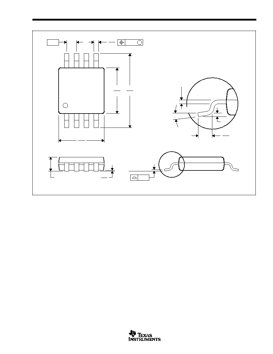
PACKAGE DRAWING
DGK (R-PDSO-G8)
PLASTIC SMALL-OUTLINE PACKAGE
0,69
0,41
0,25
0,15 NOM
Gage Plane
4073329/C 08/01
4,98
0,25
5
3,05
4,78
2,95
8
4
3,05
2,95
1
0,38
1,07 MAX
Seating Plane
0,65
M
0,08
0
�
� 6
�
0,10
0,15
0,05
NOTES: A. All linear dimensions are in millimeters.
B. This drawing is subject to change without notice.
C. Body dimensions do not include mold flash or protrusion.
D. Falls within JEDEC MO-187

PACKAGING INFORMATION
ORDERABLE DEVICE
STATUS(1)
PACKAGE TYPE
PACKAGE DRAWING
PINS
PACKAGE QTY
DAC8532IDGK
ACTIVE
VSSOP
DGK
8
80
DAC8532IDGKR
ACTIVE
VSSOP
DGK
8
2500
(1) The marketing status values are defined as follows:
ACTIVE: Product device recommended for new designs.
LIFEBUY: TI has announced that the device will be discontinued, and a lifetime-buy period is in effect.
NRND: Not recommended for new designs. Device is in production to support existing customers, but TI does not recommend using this part in
a new design.
PREVIEW: Device has been announced but is not in production. Samples may or may not be available.
OBSOLETE: TI has discontinued the production of the device.
PACKAGE OPTION ADDENDUM
www.ti.com
3-Oct-2003

IMPORTANT NOTICE
Texas Instruments Incorporated and its subsidiaries (TI) reserve the right to make corrections, modifications,
enhancements, improvements, and other changes to its products and services at any time and to discontinue
any product or service without notice. Customers should obtain the latest relevant information before placing
orders and should verify that such information is current and complete. All products are sold subject to TI's terms
and conditions of sale supplied at the time of order acknowledgment.
TI warrants performance of its hardware products to the specifications applicable at the time of sale in
accordance with TI's standard warranty. Testing and other quality control techniques are used to the extent TI
deems necessary to support this warranty. Except where mandated by government requirements, testing of all
parameters of each product is not necessarily performed.
TI assumes no liability for applications assistance or customer product design. Customers are responsible for
their products and applications using TI components. To minimize the risks associated with customer products
and applications, customers should provide adequate design and operating safeguards.
TI does not warrant or represent that any license, either express or implied, is granted under any TI patent right,
copyright, mask work right, or other TI intellectual property right relating to any combination, machine, or process
in which TI products or services are used. Information published by TI regarding third-party products or services
does not constitute a license from TI to use such products or services or a warranty or endorsement thereof.
Use of such information may require a license from a third party under the patents or other intellectual property
of the third party, or a license from TI under the patents or other intellectual property of TI.
Reproduction of information in TI data books or data sheets is permissible only if reproduction is without
alteration and is accompanied by all associated warranties, conditions, limitations, and notices. Reproduction
of this information with alteration is an unfair and deceptive business practice. TI is not responsible or liable for
such altered documentation.
Resale of TI products or services with statements different from or beyond the parameters stated by TI for that
product or service voids all express and any implied warranties for the associated TI product or service and
is an unfair and deceptive business practice. TI is not responsible or liable for any such statements.
Following are URLs where you can obtain information on other Texas Instruments products and application
solutions:
Products
Applications
Amplifiers
amplifier.ti.com
Audio
www.ti.com/audio
Data Converters
dataconverter.ti.com
Automotive
www.ti.com/automotive
DSP
dsp.ti.com
Broadband
www.ti.com/broadband
Interface
interface.ti.com
Digital Control
www.ti.com/digitalcontrol
Logic
logic.ti.com
Military
www.ti.com/military
Power Mgmt
power.ti.com
Optical Networking
www.ti.com/opticalnetwork
Microcontrollers
microcontroller.ti.com
Security
www.ti.com/security
Telephony
www.ti.com/telephony
Video & Imaging
www.ti.com/video
Wireless
www.ti.com/wireless
Mailing Address:
Texas Instruments
Post Office Box 655303 Dallas, Texas 75265
Copyright
2003, Texas Instruments Incorporated