Burr Brown Products
from Texas Instruments
FEATURES
DESCRIPTION
APPLICATIONS
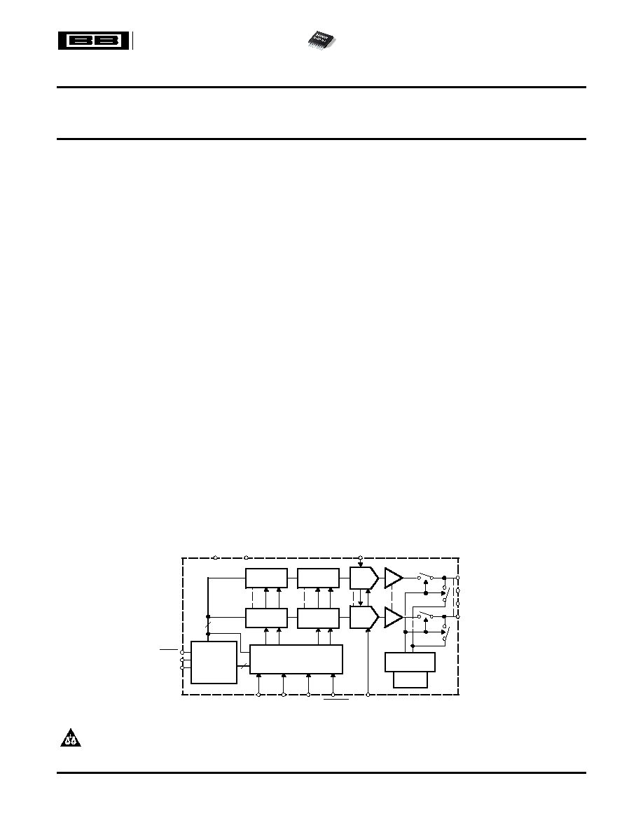
DAC
Register D
Data
Buffer A
DAC
Register A
DAC A
Data
Buffer D
DAC D
Buffer
Control
Register
Control
24-Bit
Serial-to-
Parallel Shift
Register
18
8
Power-Down
Control Logic
Resistor
Network
AV
DD
IOV
DD
V
ref
H
V
OUT
A
V
OUT
B
V
OUT
C
V
OUT
D
V
ref
L
ENABLE
LDAC
A1
A0
SYNC
SCLK
D
IN
DAC8554
SLAS431A ≠ JUNE 2005 ≠ REVISED AUGUST 2005
16-BIT, QUAD CHANNEL, ULTRALOW GLITCH, VOLTAGE OUTPUT
DIGITAL-TO-ANALOG CONVERTER
∑
Relative Accuracy: 12 LSB (Max)
The DAC8554 is a 16-bit, quad channel, voltage
output, digital-to-analog converter (DAC), offering
∑
Glitch Energy: 0.15 nV-s
low-power
operation
and
a
flexible
serial
host
∑
Power Supply: +2.7 V to +5.5 V
interface. It offers monotonicity, good linearity, and
∑
MicroPower Operation: 850 µA at 5 V
exceptionally low glitch. Each on-chip precision out-
∑
16-Bit Monotonic Over Temperature
put amplifier allows rail-to-rail output swing to be
achieved over the supply range of 2.7 V to 5.5 V. The
∑
Settling Time: 10 µs to
±
0.003% FSR
device supports a standard 3-wire serial interface
∑
Ultra-Low AC Crosstalk: ≠100 dB Typ
capable of operating with input data clock frequencies
∑
Power-On Reset to Zero-Scale
up to 50 MHz for IOV
DD
= 5 V.
∑
On-Chip Output Buffer Amplifier With
The DAC8554 requires an external reference voltage
Rail-to-Rail Operation
to set the output range of each DAC channel. Also
incorporated into the device is a power-on reset
∑
Double Buffered Input Architecture
circuit which ensures that the DAC outputs power up
∑
Simultaneous or Sequential Output Update
at zero-scale and remain there until a valid write
and Power-Down
takes place. The DAC8554 provides a per channel
∑
16-Channel Broadcast Capability
power-down
feature,
accessed
over
the
serial
interface, that reduces the current consumption to
∑
Schmitt-Triggered Inputs
200 nA per channel at 5 V.
∑
SPI Compatible Serial Interface: Up to 50 MHz
The low-power consumption of this device in normal
∑
1.8 V to 5.5 V Logic Compatibility
operation makes it ideally suited to portable battery-
∑
Available in a TSSOP-16 Package
operated equipment and other low-power appli-
cations. The power consumption is 4.25 mW at 5 V,
reducing to 4 µW in power-down mode.
∑
Portable Instrumentation
The DAC8554 is available in a TSSOP-16 package
∑
Closed-Loop Servo-Control
with a specified operating temperature range of
∑
Process Control
≠40
∞
C to 105
∞
C.
∑
Data Acquisition Systems
∑
Programmable Attenuation
∑
PC Peripherals
Please be aware that an important notice concerning availability, standard warranty, and use in critical applications of Texas
Instruments semiconductor products and disclaimers thereto appears at the end of this data sheet.
SPI, QSPI are trademarks of Motorola.
Microwire is a trademark of National Semiconductor.
PRODUCTION DATA information is current as of publication date.
Copyright © 2005, Texas Instruments Incorporated
Products conform to specifications per the terms of the Texas
Instruments standard warranty. Production processing does not
necessarily include testing of all parameters.

www.ti.com
ABSOLUTE MAXIMUM RATINGS
(1)
ELECTRICAL CHARACTERISTICS
DAC8554
SLAS431A ≠ JUNE 2005 ≠ REVISED AUGUST 2005
This integrated circuit can be damaged by ESD. Texas Instruments recommends that all integrated
circuits be handled with appropriate precautions. Failure to observe proper handling and installation
procedures can cause damage.
ESD damage can range from subtle performance degradation to complete device failure. Precision
integrated circuits may be more susceptible to damage because very small parametric changes could
cause the device not to meet its published specifications. This device is rated at 1500 V HBM and 1000
V CDM.
PACKAGING/ORDERING INFORMATION
PACKAGE
PACKAGE
SPECIFICATION
PACKAGE
ORDERING
TRANSPORT
PRODUCT
LEAD
DESIGNATOR
(1)
TEMPERATURE RANGE
MARKING
NUMBER
MEDIA, QUANTITY
DAC8554IPW
Tube, 90
DAC8554
TSSOP-16
PW
≠40
∞
C TO 105
∞
C
D8554
DAC8554IPWR
Tape and Reel, 2000
(1)
For the most current specifications and package information, refer to our web site at www.ti.com.
UNIT
AV
DD
to GND
≠0.3 V to 6 V
Digital input voltage to GND
≠0.3 V to AV
DD
+ 0.3 V
V
O(A)
to V
O(D)
to GND
≠0.3 V to AV
DD
+ 0.3 V
Operating temperature range
≠40
∞
C to 105
∞
C
Storage temperature range
≠65
∞
C to 150
∞
C
Junction temperature range (T
J
max)
150
∞
C
Power dissipation
(T
J
max ≠ T
A
)/
JA
JA
Thermal impedance
118
∞
C/W
JC
Thermal impedance
29
∞
C/W
Vapor phase (60 s)
215
∞
C
Lead temperature, soldering
Infrared (15 s)
220
∞
C
(1)
Stresses above those listed under absolute maximum ratings may cause permanent damage to the device. Exposure to absolute
maximum conditions for extended periods may affect device reliability.
over operating free-air temperature range (unless otherwise noted)
PARAMETER
TEST CONDITIONS
MIN
TYP
MAX
UNIT
STATIC PERFORMANCE
(1)
Resolution
16
Bits
Relative accuracy
Measured by line passing through codes 485 and
±4
±12
LSB
64741
Differential nonlinearity
16-bit Monotonic
±
0.25
±
1
LSB
Zero-scale error
Measured by line passing through codes 485 and
±2
±12
mV
64741
Zero-scale error drift
±5
µV/
∞
C
Full-scale error
Measured by line passing through codes 485 and
±0.3
±0.5
% of FSR
64741, AV
DD
= 5 V, V
ref
= 4.99 V
Gain error
Measured by line passing through codes 485 and
±0.05
±0.15
% of FSR
64741, AV
DD
= 5 V
Gain temperature coefficient
±
1
ppm of FSR/
∞
C
8
mV
Power Supply Rejection Ratio
R
L
= 2 k
, C
L
= 200 pF
(PSRR)
0.75
mV/V
(1)
Linearity calculated using a reduced code range of 485 to 64741; output unloaded.
2
www.ti.com
DAC8554
SLAS431A ≠ JUNE 2005 ≠ REVISED AUGUST 2005
ELECTRICAL CHARACTERISTICS (continued)
over operating free-air temperature range (unless otherwise noted)
PARAMETER
TEST CONDITIONS
MIN
TYP
MAX
UNIT
OUTPUT CHARACTERISTICS
(2)
Output voltage range
0
V
ref
H
V
Output voltage settling time
To ±0.003% FSR, 0200
H
to FD00
H
, R
L
= 2 k
, 0 pF
8
10
µs
< C
L
< 200 pF
R
L
= 2 k
, C
L
= 500 pF
12
µs
Slew rate
1.8
V/µs
R
L
=
470
pF
Capacitive load stability
R
L
= 2 k
1000
pF
Code change glitch impulse
1 LSB change around major carry
0.15
nV-s
Digital feedthrough
0.15
DC crosstalk
Full-scale swing on adjacent channel. AV
DD
= 5 V,
0.25
LSB
V
ref
= 4.096 V
AC crosstalk
1 kHz sine wave
≠100
dB
DC output impedance
At mid-point input
1
AV
DD
= 5 V
50
Short-circuit current
mA
AV
DD
= 3 V
20
Coming out of power-down mode AV
DD
= 5 V
2.5
Power-up time
µs
Coming out of power-down mode AV
DD
= 3 V
5
AC PERFORMANCE
SNR (1st 19 harmonics removed)
95
THD
-85
BW = 20 kHz, AV
DD
= 5 V, F
OUT
= 1 kHz
dB
SFDR
87
SINAD
84
REFERENCE INPUT
V
ref(H)
Voltage
V
ref(L)
< V
ref(H)
, AV
DD
- (V
ref(H)
+ V
ref(L)
) /2 > 1.2 V
0
AV
DD
V
V
ref(L)
Voltage
V
ref(L)
< V
ref(H)
, AV
DD
- (V
ref(H)
+ V
ref(L)
) /2 > 1.2 V
0
AV
DD
/2
V
V
ref(L)
= GND, V
ref(H)
= AV
DD
= 5 V
180
250
µA
Reference input current
V
ref(L)
= GND, V
ref(H)
= AV
DD
= 3 V
120
200
µA
Reference input impedance
V
ref(L)
< V
ref(H)
31
k
LOGIC INPUTS
(3)
0.3
◊
2.7 V
IOV
DD
5.5 V
I0V
DD
V
I(L)
, logic input LOW voltage
V
0.1
◊
1.8 V
IOV
DD
2.7 V
I0V
DD
0.7
◊
2.7
IOV
DD
5.5 V
I0V
DD
V
I(H)
, logic input HIGH voltage
V
0.95
◊
1.8
IOV
DD
< 2.7 V
I0V
DD
Pin capacitance
3
pF
POWER REQUIREMENTS
AV
DD
2.7
5.5
V
IOV
DD
1.8
5.5
AI
DD
(normal mode)
Input code = 32768, reference current included, no
load
(2)
Ensured by design and characterization, not production tested.
(3)
Ensured by design and characterization, not production tested.
3

www.ti.com
PIN CONFIGURATION
V
OUT
A
V
OUT
B
V
REF
H
AV
DD
V
REF
L
GND
V
OUT
C
V
OUT
D
LDAC
ENABLE
A1
A0
IOV
DD
D
IN
SCLK
SYNC
1
2
3
4
5
6
7
8
16
15
14
13
12
11
10
9
DAC8554
DAC8554
SLAS431A ≠ JUNE 2005 ≠ REVISED AUGUST 2005
ELECTRICAL CHARACTERISTICS (continued)
over operating free-air temperature range (unless otherwise noted)
PARAMETER
TEST CONDITIONS
MIN
TYP
MAX
UNIT
IOI
DD
10
20
µA
AV
DD
= 3.6 V to 5.5 V
V
IH
= IOV
DD
and V
IL
= GND
0.65
1.0
mA
AV
DD
= 2.7 V to 3.6 V
0.6
0.96
AI
DD
(all power-down modes)
AV
DD
= 3.6 V to 5.5 V
V
IH
= IOV
DD
and V
IL
= GND
0.2
2
µA
AV
DD
= 2.7 V to 3.6 V
0.05
2
POWER EFFICIENCY
I
OUT
/I
DD
I
L
= 2 mA, AV
DD
= 5 V
89%
TEMPERATURE RANGE
Specified performance
≠40
105
∞
C
PIN DESCRIPTIONS
PIN
NAME
DESCRIPTION
1
V
OUT
A
Analog output voltage from DAC A.
2
V
OUT
B
Analog output voltage from DAC B.
3
V
ref
H
Positive reference voltage input.
4
AV
DD
Power supply input, 2.7 V to 5.5 V.
5
V
ref
L
Negative reference voltage input.
6
GND
Ground reference point for all circuitry on the part.
7
V
OUT
C
Analog output voltage DAC C.
8
V
OUT
D
Analog output voltage DAC D.
Level-triggered control input (active LOW). This is the frame synchronization signal for the input data. When
SYNC goes LOW, it enables the input shift register and data is transferred in on the falling edges of the
9
SYNC
following clocks. The DAC is updated following the 24th clock (unless SYNC is taken HIGH before this edge
in which case the rising edge of SYNC acts as an interrupt and the write sequence is ignored by the
DAC8554).
10
SCLK
Serial clock input. Data can be transferred at rates up to 50 MHz.
Serial data input. Data is clocked into the 24-bit input shift register on each falling edge of the serial clock
11
D
IN
input.
12
IOV
DD
Digital input-output power supply
13
A0
Address 0 -- sets device address, see Table 2
14
A1
Address 1 -- sets device address, see Table 2
15
ENABLE
Active LOW, ENABLE LOW connects the SPI interface to the serial port.
4
www.ti.com
TIMING REQUIREMENTS
(1) (2)
SERIAL WRITE OPERATION
SCLK
1
24
SYNC
D
IN
DB23
DB0
DB23
t
8
t
3
t
2
t
7
t
4
t
5
t
6
t
1
t
9
DAC8554
SLAS431A ≠ JUNE 2005 ≠ REVISED AUGUST 2005
PIN DESCRIPTIONS (continued)
PIN
NAME
DESCRIPTION
16
LDAC
Load DACs, rising edge triggered, loads all DAC registers.
AV
DD
= 2.7 V to 5.5 V, all specifications ≠40
∞
C to 105
∞
C (unless otherwise noted)
PARAMETER
TEST CONDITIONS
MIN
TYP
MAX
UNIT
IOV
DD
= AV
DD
= 2.7 V to 3.6 V
40
t
1
(3)
SCLK cycle time
ns
IOV
DD
= AV
DD
= 3.6 V to 5.5 V
20
IOV
DD
= AV
DD
= 2.7 V to 3.6 V
20
t
2
SCLK HIGH time
ns
IOV
DD
= AV
DD
= 3.6 V to 5.5 V
10
IOV
DD
= AV
DD
= 2.7 V to 3.6 V
20
t
3
SCLK LOW time
ns
IOV
DD
= AV
DD
= 3.6 V to 5.5 V
10
IOV
DD
= AV
DD
= 2.7 V to 3.6 V
0
t
4
SYNC falling edge to SCLK rising edge setup time
ns
IOV
DD
= AV
DD
= 3.6 V to 5.5 V
0
IOV
DD
= AV
DD
= 2.7 V to 3.6 V
5
t
5
Data setup time
ns
IOV
DD
= AV
DD
= 3.6 V to 5.5 V
5
IOV
DD
= AV
DD
= 2.7 V to 3.6 V
4.5
t
6
Data hold time
ns
IOV
DD
= AV
DD
= 3.6 V to 5.5 V
4.5
IOV
DD
= AV
DD
= 2.7 V to 3.6 V
0
t
7
24th SCLK falling edge to SYNC rising edge
ns
IOV
DD
= AV
DD
= 3.6 V to 5.5 V
0
IOV
DD
= AV
DD
= 2.7 V to 3.6 V
40
t
8
Minimum SYNC HIGH time
ns
IOV
DD
= AV
DD
= 3.6 V to 5.5 V
20
t
9
24th SCLK falling edge to SYNC falling edge
IOV
DD
= AV
DD
= 2.7 V to 5.5 V
130
ns
(1)
All input signals are specified with t
R
= t
F
= 3 ns (10% to 90% of AV
DD
) and timed from a voltage level of (V
IL
+ V
IH
)/2.
(2)
See Serial Write Operation timing diagram.
(3)
Maximum SCLK frequency is 50 MHz at IOV
DD
= AV
DD
= 3.6 V to 5.5 V and 25 MHz at IOV
DD
= AV
DD
= 2.7 V to 3.6 V.
5
www.ti.com
TYPICAL CHARACTERISTICS
-8
-6
-4
-2
0
2
4
6
8
LE (LSB)
-1
-0.5
0
0.5
1
0
8192
16384
24576
32768 40960
49152
57344 65536
Digital Input Code
DLE (LSB)
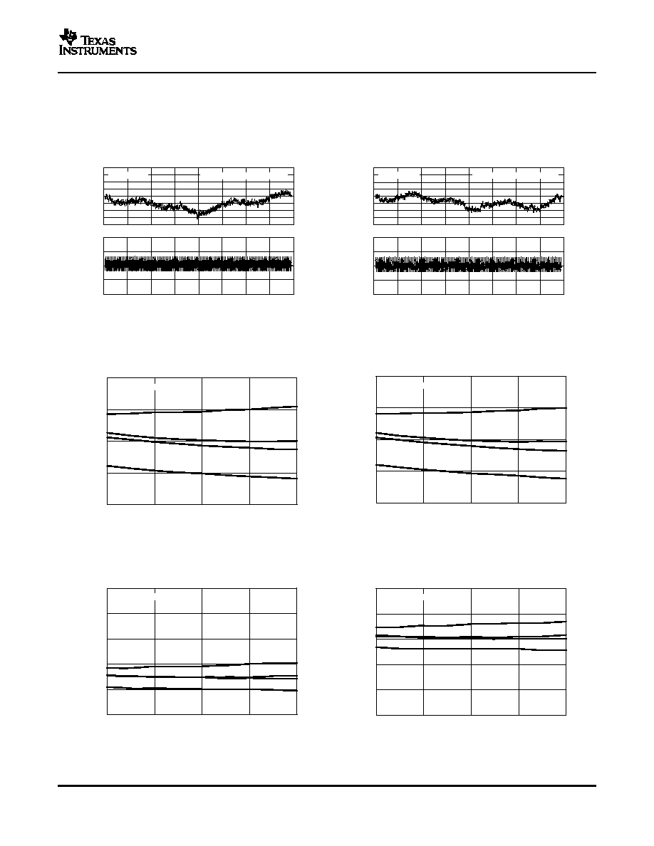
Channel A
AV
DD
= 5 V, V
ref
= 4.99 V
-8
-6
-4
-2
0
2
4
6
8
LE (LSB)
-1
-0.5
0
0.5
1
0
8192
16384 24576
32768 40960
49152 57344 65536
Digital Input Code
DLE (LSB)
Channel B
AV
DD
= 5 V, V
ref
= 4.99 V
-8
-6
-4
-2
0
2
4
6
8
LE (LSB)
-1
-0.5
0
0.5
1
0
8192
16384 24576
32768 40960
49152
57344 65536
Digital Input Code
DLE (LSB)
Channel C
AV
DD
= 5 V, V
ref
= 4.99 V
-8
-6
-4
-2
0
2
4
6
8
LE (LSB)
-1
-0.5
0
0.5
1
0
8192
16384
24576
32768 40960
49152
57344
65536
Digital Input Code
DLE (LSB)
Channel D
AV
DD
= 5 V, V
ref
= 4.99 V
-8
-6
-4
-2
0
2
4
6
8
LE (LSB)
-1
-0.5
0
0.5
1
0
8192
16384 24576
32768 40960
49152
57344 65536
Digital Input Code
DLE (LSB)
Channel B
AV
DD
= 2.7 V, V
ref
= 2.69 V
-8
-6
-4
-2
0
2
4
6
8
LE (LSB)
-1
-0.5
0
0.5
1
0
8192
16384 24576
32768 40960
49152
57344
65536
Digital Input Code
DLE (LSB)
Channel A
AV
DD
= 2.7 V, V
ref
= 2.69 V
DAC8554
SLAS431A ≠ JUNE 2005 ≠ REVISED AUGUST 2005
At T
A
= 25
∞
C, unless otherwise noted
LINEARITY ERROR AND DIFFERENTIAL
LINEARITY ERROR AND DIFFERENTIAL
LINEARITY ERROR
LINEARITY ERROR
vs
vs
DIGITAL INPUT CODE
DIGITAL INPUT CODE
Figure 1.
Figure 2.
LINEARITY ERROR AND DIFFERENTIAL
LINEARITY ERROR AND DIFFERENTIAL
LINEARITY ERROR
LINEARITY ERROR
vs
vs
DIGITAL INPUT CODE
DIGITAL INPUT CODE
Figure 3.
Figure 4.
LINEARITY ERROR AND DIFFERENTIAL
LINEARITY ERROR AND DIFFERENTIAL
LINEARITY ERROR
LINEARITY ERROR
vs
vs
DIGITAL INPUT CODE
DIGITAL INPUT CODE
Figure 5.
Figure 6.
6
www.ti.com
-8
-6
-4
-2
0
2
4
6
8
LE (LSB)
-1
-0.5
0
0.5
1
0
8192
16384 24576
32768 40960 49152
57344 65536
Digital Input Code
DLE (LSB)
Channel C
AV
DD
= 2.7 V, V
ref
= 2.69 V
-8
-6
-4
-2
0
2
4
6
8
LE (LSB)
-1
-0.5
0
0.5
1
0
8192
16384 24576 32768
40960
49152 57344 65536
Digital Input Code
DLE (LSB)
Channel D
AV
DD
= 2.7 V, V
ref
= 2.69 V
-5
-2.5
0
2.5
5
-40
0
40
80
120
Error (mV)
CH B
CH D
CH A
CH C
AV
DD
= 2.7 V, V
ref
= 2.69 V
T
A
- Temperature -
∞
C
-5
-2.5
0
2.5
5
-40
0
40
80
120
Error (mV)
CH B
CH A
CH C
CH D
AV
DD
= 5 V, V
ref
= 4.99 V
T
A
- Temperature -
∞
C
-25
-20
-15
-10
-5
0
-40
0
40
80
120
Error (mV)
CH A
CH D
CH B
CH C
AV
DD
= 5 V, V
ref
= 4.99 V
T
A
- Temperature -
∞
C
-25
-20
-15
-10
-5
0
-40
0
40
80
120
Error (mV)
CH A
CH B
CH C
CH D
AV
DD
= 2.7 V, V
ref
= 2.69 V
T
A
- Temperature -
∞
C
DAC8554
SLAS431A ≠ JUNE 2005 ≠ REVISED AUGUST 2005
TYPICAL CHARACTERISTICS (continued)
At T
A
= 25
∞
C, unless otherwise noted
LINEARITY ERROR AND DIFFERENTIAL
LINEARITY ERROR AND DIFFERENTIAL
LINEARITY ERROR
LINEARITY ERROR
vs
vs
DIGITAL INPUT CODE
DIGITAL INPUT CODE
Figure 7.
Figure 8.
ZERO-SCALE ERROR
ZERO-SCALE ERROR
vs
vs
TEMPERATURE
TEMPERATURE
Figure 9.
Figure 10.
FULL-SCALE ERROR
FULL-SCALE ERROR
vs
vs
TEMPERATURE
TEMPERATURE
Figure 11.
Figure 12.
7

www.ti.com
0
0.025
0.050
0.075
0.100
0.125
0.150
0
2
4
6
8
10
V
DD
= 5.5 V
V
DD
= 2.7 V
V
OUT
(V)
I
SINK
(mA)
V
ref
= AV
DD
-10 mV
DAC Loaded With 0000
H
4
4.4
4.8
5.2
5.6
6
0
2
4
6
8
10
V
DD
= 5.5 V
V
ref =
AV
DD
-10 mV
DAC Loaded With FFFF
H
V
OUT
(V)
I
SIOURCE
(mA)
1.5
1.8
2.1
2.4
2.7
3
0
2
4
6
8
10
AV
DD
= 2.7 V
V
ref =
AV
DD
-10 mV
DAC Loaded With FFFF
H
V
OUT
(V)
I
SIOURCE
(mA)
0
200
400
600
800
1000
1200
0
8192
16384 24576 32768 40960
49152
57344 65536
Digital Input Code
I DD
(
µ
A
)
AV
DD =
V
ref
= 5.5 V
AV
DD =
V
ref
= 2.7 V
Reference Current Included
600
650
700
750
800
850
900
2.7
3.05
3.4
3.75
4.1
4.45
4.8
5.15
5.5
I DD
(
µ
A
)
V
DD
(V)
V
ref =
AV
DD
All DACs Powered,
Reference Current Included, No Load
0
200
400
600
800
1000
1200
-40
0
40
80
120
I DD
(
µ
A
)
AV
DD =
V
ref
= 5.5 V
AV
DD =
V
ref
= 2.7 V
Reference Current Included
T
A
- Temperature -
∞
C
DAC8554
SLAS431A ≠ JUNE 2005 ≠ REVISED AUGUST 2005
TYPICAL CHARACTERISTICS (continued)
At T
A
= 25
∞
C, unless otherwise noted
SINK CURRENT CAPABILITY (ALL CHANNELS)
SOURCE CURRENT CAPABILITY (ALL CHANNELS)
Figure 13.
Figure 14.
SOURCE CURRENT CAPABILITY (ALL CHANNELS)
SUPPLY CURRENT
vs
DIGITAL INPUT CODE
Figure 15.
Figure 16.
SUPPLY CURRENT
SUPPLY CURRENT
vs
vs
FREE-AIR TEMPERATURE
SUPPLY VOLTAGE
Figure 17.
Figure 18.
8
www.ti.com
0
400
800
1200
1600
2000
0
1
2
3
4
5
IOV
DD
= AV
DD
= V
ref
= 5 V
I DD
(
µ
A
)
T
A
= 25
∞
C, SYNC Input (All Other Inputs = GND
CHA Powered Up; All Other Channels in Powerdown
Reference Current Included
V
LOGIC
(V)
0
200
400
600
800
0
0.5
1
1.5
2
2.5
I DD
(
µ
A
)
T
A
= 25
∞
C, SYNC Input (All Other Inputs = GND
CHA Powered Up; All Other Channels in Powerdown
Reference Current Included
V
LOGIC
(V)
IOV
DD
= AV
DD
= V
ref
= 2.7 V
0
500
1000
1500
725
750
775
800
825
850
875
900
925
950
975
Frequency
I
DD
(
µ
A)
AV
DD =
V
ref
= 5 V
Reference Current Included
0
500
1000
1500
600 625 650 675 700 725 750 775 800 825 850 875
Frequency
I
DD
(
µ
A)
AV
DD =
V
ref
= 2.7 V
Reference Current Included
-100
-90
-80
-70
-60
-50
-40
0
1
2
3
4
5
Output Tone (kHz)
THD (dB)
THD
2nd Harmonic
3rd Harmonic
AV
DD
= V
ref
= 5 V,
-1 dB FSR Digital Input, F
s
= 1 MSPS
Measurement Bandwidth = 20 kHz
-130
-110
-90
-70
-50
-30
-10
0
5000
10000
15000
20000
Frequency - Hz
Gain dB
AV
DD
= 5 V,
V
ref
= 4.096,
f
clk
= 1 MSPS,
F
out
= 1 kHz,
THD = 79 dB,
SNR = 96 dB
DAC8554
SLAS431A ≠ JUNE 2005 ≠ REVISED AUGUST 2005
TYPICAL CHARACTERISTICS (continued)
At T
A
= 25
∞
C, unless otherwise noted
SUPPLY CURRENT
SUPPLY CURRENT
vs
vs
LOGIC INPUT VOLTAGE
LOGIC INPUT VOLTAGE
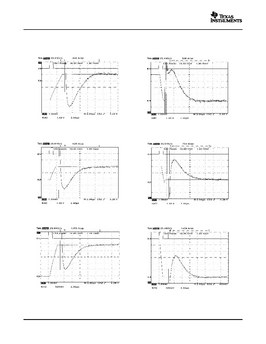
Figure 19.
Figure 20.
HISTOGRAM OF CURRENT CONSUMPTION
HISTOGRAM OF CURRENT CONSUMPTION
Figure 21.
Figure 22.
POWER SPECTRAL DENSITY
TOTAL HARMONIC DISTORTION
vs
OUTPUT FREQUENCY
Figure 23.
Figure 24.
9
www.ti.com
Time (2
µ
s/div)
AV
DD
= 5 V,
V
ref
= 4.096 V,
From Code: FFFF
To Code: 0000
Zoomed Falling Edge
1 mV/div
Trigger Pulse
5 V/div
Falling
Edge
1 V/div
Time (2
µ
s/div)
AV
DD
= 5 V,
V
ref
= 4.096 V,
From Code: 0000
To Code: FFFF
Zoomed Rising Edge
1 mV/div
Trigger Pulse
5 V/div
Rising
Edge
1 V/div
Time (2
µ
s/div)
AV
DD
= 5 V,
V
ref
= 4.096 V,
From Code: 4000
To Code: CFFF
Zoomed Rising Edge
1 mV/div
Trigger Pulse
5 V/div
Rising
Edge
1 V/div
Time (2
µ
s/div)
AV
DD
= 5 V,
V
ref
= 4.096 V,
From Code: CFFF
To Code: 4000
Zoomed Falling Edge
1 mV/div
Trigger Pulse
5 V/div
Falling
Edge
1 V/div
Time (2
µ
s/div)
AV
DD
= 2.7 V,
V
ref
= 2.5 V,
From Code: 0000
To Code: FFFF
Zoomed Rising Edge
1 mV/div
Trigger Pulse
2.7 V/div
Rising
Edge
0.5 V/div
Time (2
µ
s/div)
AV
DD
= 2.7 V,
V
ref
= 2.5 V,
From Code: FFFF
To Code: 0000
Zoomed Falling Edge
1 mV/div
Trigger Pulse
2.7 V/div
Falling
Edge
0.5 V/div
DAC8554
SLAS431A ≠ JUNE 2005 ≠ REVISED AUGUST 2005
TYPICAL CHARACTERISTICS (continued)
At T
A
= 25
∞
C, unless otherwise noted
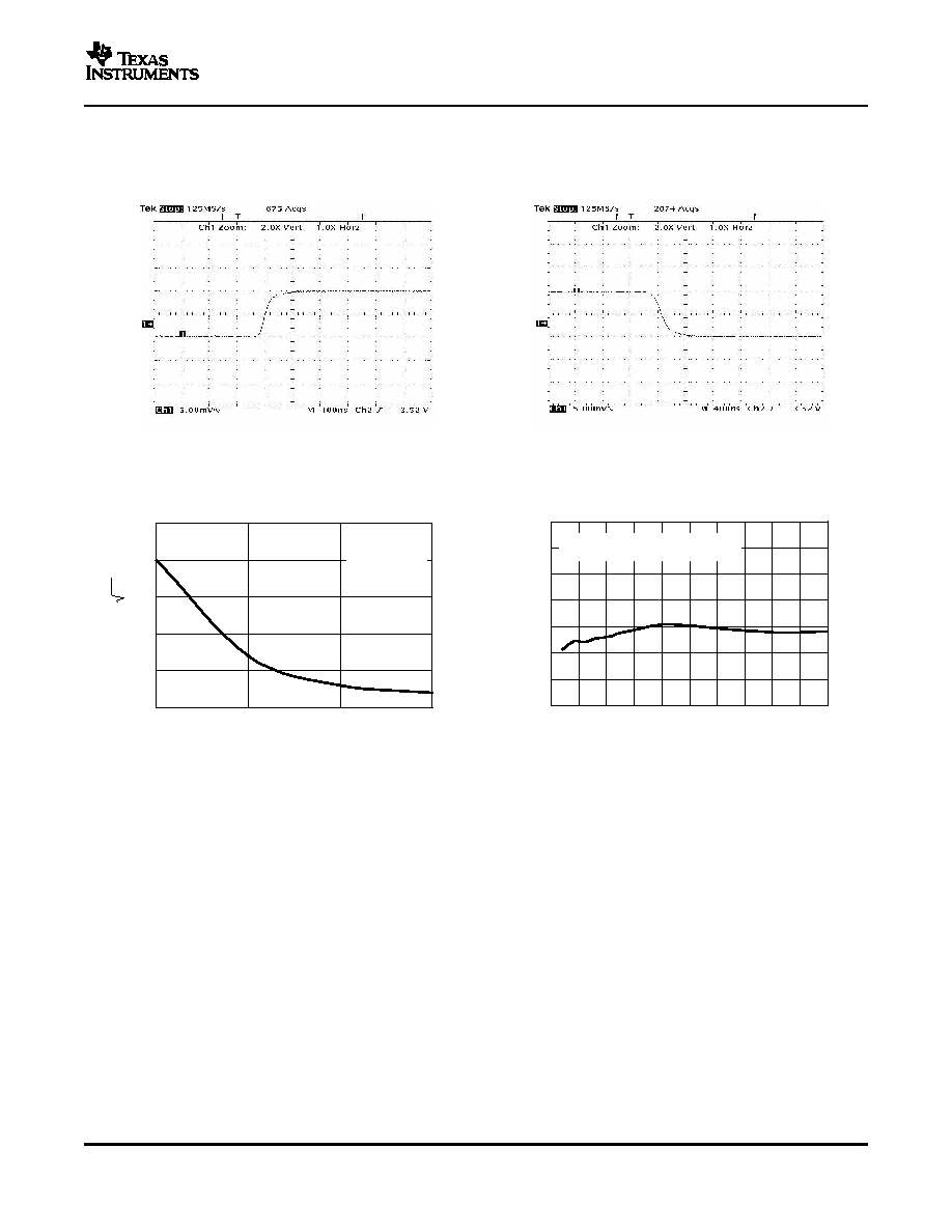
FULL-SCALE SETTLING TIME: 5 V RISING EDGE
FULL-SCALE SETTLING TIME: 5 V FALLING EDGE
Figure 25.
Figure 26.
HALF-SCALE SETTLING TIME: 5 V RISING EDGE
HALF-SCALE SETTLING TIME: 5 V FALLING EDGE
Figure 27.
Figure 28.
FULL-SCALE SETTLING TIME: 2.7 V RISING EDGE
FULL-SCALE SETTLING TIME: 2.7 V FALLING EDGE
Figure 29.
Figure 30.
10

www.ti.com
AV
DD
= 2.7 V,
V
ref
= 2.5 V,
From Code: CFFF
To Code: 4000
Zoomed Falling Edge
1 mV/div
Trigger Pulse
2.7 V/div
Falling
Edge
0.5 V/div
Time (2
µ
s/div)
Trigger Pulse
2.7 V/div
Zoomed Rising Edge
1 mV / div
V
DD
= 2.7 V
V
REF
= 2.5 V
From code; 4000
To code: CFFF
Rising
Edge
0.5 V/div
Time - 2
m
s/div
AV
DD
= 5 V,
V
ref
= 4.096 V
From Code: 8000
To Code: 7FFF
Glitch: 0.16 nV-s
Measured Worst Case
Time 400 ns/div
V
OUT
(500
m
V/div)
AV
DD
= 5 V,
V
ref
= 4.096 V
From Code: 7FFF
To Code: 8000
Glitch: 0.08 nV-s
Time 400 ns/div
V
OUT
(500
m
V/div)
AV
DD
= 5 V,
V
ref
= 4.096 V
From Code: 8010
To Code: 8000
Glitch: 0.08 nV-s
Time 400 ns/div
V
OUT
m
V/div)
(500
AV
DD
= 5 V,
V
ref
= 4.096 V
From Code: 8000
To Code: 8010
Glitch: 0.04 nV-s
Time 400 ns/div
V
OUT
(500
m
V/div)
DAC8554
SLAS431A ≠ JUNE 2005 ≠ REVISED AUGUST 2005
TYPICAL CHARACTERISTICS (continued)
At T
A
= 25
∞
C, unless otherwise noted
HALF-SCALE SETTLING TIME: 2.7 V RISING EDGE
HALF-SCALE SETTLING TIME: 2.7 V FALLING EDGE
Figure 31.
Figure 32.
GLITCH ENERGY: 5 V, 1 LSB STEP, RISING EDGE
GLITCH ENERGY: 5 V, 1 LSB STEP, FALLING EDGE
Figure 33.
Figure 34.
GLITCH ENERGY: 5 V, 16 LSB STEP, RISING EDGE
GLITCH ENERGY: 5 V, 16 LSB STEP, FALLING EDGE
Figure 35.
Figure 36.
11

www.ti.com
AV
DD
= 5 V,
V
ref
= 4.096 V
From Code: 80FF
To Code: 8000
Glitch: Not Detected
Theoretical Worst Case
Time 400 ns/div
V
OUT
(5 mV/div)
AV
DD
= 5 V,
V
ref
= 4.096 V
From Code: 8000
To Code: 80FF
Glitch: Not Detected
Theoretical Worst Case
Time 400 ns/div
V
OUT
(5 mV/div)
AV
DD
= 2,7 V,
V
ref
= 2.5 V
From Code: 7FFF
To Code: 8000
Glitch: 0.08 nV-s
Time 400 ns/div
V
OUT
(200
m
V/div)
AV
DD
= 2.7 V,
V
ref
= 2.5 V
From Code: 8000
To Code: 7FFF
Glitch: 0.16 nV-s
Measured Worst Case
Time 400 ns/div
V
OUT
(200
m
V/div)
AV
DD
= 2.7 V,
V
ref
= 2.5 V
From Code: 8000
To Code: 8010
Glitch: 0.04 nV-s
Time 400 ns/div
V
OUT
(200 uV/div)
AV
DD
= 2.7 V,
V
ref
= 2.5 V
From Code: 8010
To Code: 8000
Glitch: 0.12 nV-s
Time 400 ns/div
V/div)
V
OUT
(200 uV/div)
DAC8554
SLAS431A ≠ JUNE 2005 ≠ REVISED AUGUST 2005
TYPICAL CHARACTERISTICS (continued)
At T
A
= 25
∞
C, unless otherwise noted
GLITCH ENERGY: 5 V, 256 LSB STEP, RISING EDGE
GLITCH ENERGY: 5 V, 256 LSB STEP, FALLING EDGE
Figure 37.
Figure 38.
GLITCH ENERGY:; 2.7 V, 1 LSB STEP, RISING EDGE
GLITCH ENERGY: 2.7 V, 1 LSB STEP, FALLING EDGE
Figure 39.
Figure 40.
GLITCH ENERGY: 2.7 V, 16 LSB STEP, RISING EDGE
GLITCH ENERGY: 2.7 V, 16 LSB STEP, FALLING EDGE
Figure 41.
Figure 42.
12
www.ti.com
AV
DD
= 2.7 V,
V
ref
= 2.5 V
From Code: 80FF
To Code: 8000
Glitch: Not Detected
Theoretical Worst Case
Time 400 ns/div
V
OUT
(5 mV/div)
AV
DD
= 2.7 V,
V
ref
= 2.5 V
From Code: 8000
To Code: 80FF
Glitch: Not Detected
Theoretical Worst Case
Time 400 ns/div
V
OUT
(5 mV/div)
84
86
88
90
92
94
96
98
0
0.5
1
1.5
2
2.5
3
3.5
4
4.5
5
Output Tone (kHz)
SNR (dB)
AV
DD
= V
ref
= 5 V,
-1 dB FSR Digital Inputs, F
s
= 1 MSPS
Measurement Bandwidth = 20 kHz
100
150
200
250
300
350
100
1000
10000
100000
Frequency - Hz
nV/
Hz
Noise -
AV
DD
= 5 V,
V
ref
= 4.096 V,
Code = 7FFF
No Load
DAC8554
SLAS431A ≠ JUNE 2005 ≠ REVISED AUGUST 2005
TYPICAL CHARACTERISTICS (continued)
At T
A
= 25
∞
C, unless otherwise noted
GLITCH ENERGY: 2.7 V, 16 LSB STEP, RISING EDGE
GLITCH ENERGY: 2.7 V, 16 LSB STEP, FALLING EDGE
Figure 43.
Figure 44.
OUTPUT NOISE DENSITY
SIGNAL-TO-NOISE RATIO
vs
OUTPUT FREQUENCY
Figure 45.
Figure 46.
13

www.ti.com
THEORY OF OPERATION
DAC SECTION
62
V
OUT
X
+
2
V
REF
L
)
V
REF
H
*
V
REF
L
D
IN
65536
RESISTOR STRING
To Output
Amplifier
(2x Gain)
R
R
R
R
V
REF
2
V
REF
H
R
DIVIDER
V
REF
L
OUTPUT AMPLIFIER
SERIAL INTERFACE
DAC8554
SLAS431A ≠ JUNE 2005 ≠ REVISED AUGUST 2005
The architecture of each channel of the DAC8554
consists of a resistor-string DAC followed by an
output buffer amplifier.
Figure 47
shows a simplified
block diagram of the DAC architecture.
Figure 47. DAC8554 Architecture
The input coding for each device is unipolar straight
binary, so the ideal output voltage is given by:
where D
IN
= decimal equivalent of the binary code
that is loaded to the DAC register; it can range from 0
to 65535.
The resistor string section is shown in
Figure 48
. It is
simply a divide-by-2 resistor followed by a string of
Figure 48. Resistor String
resistors. The code loaded into the DAC register
determines at which node on the string the voltage is
tapped off. This voltage is then applied to the output
The write sequence begins by bringing the SYNC line
amplifier by closing one of the switches connecting
LOW. Data from the D
IN
line is clocked into the 24-bit
the string to the amplifier.
shift register on each falling edge of SCLK. The serial
clock frequency can be as high as 50 MHz, making
the DAC8554 compatible with high-speed DSPs. On
the 24th falling edge of the serial clock, the last data
Each output buffer amplifier is capable of generating
bit is clocked into the shift register and the shift
rail-to-rail voltages on its output which approaches an
register gets locked. Further clocking does not
output range of 0 V to AV
DD
(gain and offset errors
change the shift register data. Once 24 bits are
must be taken into account). Each buffer is capable
locked into the shift register, the 8 MSBs are used as
of driving a load of 2 k
in parallel with 1000 pF to
control bits and the 16 LSBs are used as data. After
GND. The source and sink capabilities of the output
receiving the 24th falling clock edge, DAC8554 de-
amplifier can be seen in the typical characteristics.
codes the 8 control bits and 16 data bits to perform
the required function, without waiting for a SYNC
rising edge. A new SPI sequence starts at the next
The DAC8554 uses a 3-wire serial interface ( SYNC,
falling edge of SYNC. A rising edge of SYNC before
SCLK, and D
IN
), which is compatible with SPITM,
the 24-bit sequence is complete resets the SPI
QSPITM, and MicrowireTM interface standards, as well
interface; no data transfer occurs.
as most DSPs. See the serial write operation timing
After the 24th falling edge of SCLK is received, the
diagram for an example of a typical write sequence.
SYNC line may be kept LOW or brought HIGH. In
either case, the minimum delay time from the 24th
falling SCLK edge to the next falling SYNC edge
must be met in order to properly begin the next cycle.
14

www.ti.com
IOV
DD
AND VOLTAGE TRANSLATORS
INPUT SHIFT REGISTER
DAC8554
SLAS431A ≠ JUNE 2005 ≠ REVISED AUGUST 2005
To assure the lowest power consumption of the
Care bit which does not affect the operation of the
device, care should be taken that the levels are as
DAC8554 and can be 1 or 0. The DAC channel select
close to each rail as possible. (Refer to the Typical
bits (DB18, DB17) control the destination of the data
Characteristics section for the Supply Current vs
(or power-down command) from DAC A through DAC
Logic Input Voltage transfer characteristic curve.
D. The final control bit, PD0 (DB16), selects the
power-down mode of the DAC8554 channels.
The DAC8554 also supports a number of different
load commands. The load commands include broad-
The IOV
DD
pin powers the digital input structures of
cast commands to address all the DAC8554s on an
the DAC8554. For single-supply operation, it can be
SPI bus. The load commands can be summarized as
tied to AV
DD
. For dual-supply operation, the IOV
DD
pin
follows:
provides interface flexibility with various CMOS logic
families and it should be connected to the logic
DB21 = 0 and DB20 = 0: Single-channel store. The
supply of the system. Analog circuits and internal
temporary register (data buffer) corresponding to a
logic of the DAC8554 use AV
DD
as the supply
DAC selected by DB18 and DB17 is updated with the
voltage. The external logic high inputs get translated
contents of SR data (or power-down).
to AV
DD
by level shifters. These level shifters use the
IOV
DD
voltage as a reference to shift the incoming
DB21 = 0 and DB20 = 1: Single-channel update. The
logic HIGH levels to AV
DD
. IOV
DD
is ensured to
temporary register and DAC register corresponding to
operate from 2.7 V to 5.5 V regardless of the AV
DD
a DAC selected by DB18 and DB17 are updated with
voltage, which ensures compatibility with various logic
the contents of SR data (or power-down).
families. Although specified down to 2.7 V, IOV
DD
will
DB21 = 1 and DB20 = 0: Simultaneous update. A
operate at as low as 1.8 V with degraded timing and
channel selected by DB18 and DB17 gets updated
temperature performance. For lowest power con-
with the SR data, and simultaneously, all the other
sumption, logic V
IH
levels should be as close as
channels get updated with previous stored data (or
possible to IOV
DD
, and logic V
IL
levels should be as
power-down) from temporary registers.
close as possible to GND voltages
DB21 = 1 and DB20 = 1: Broadcast update. All the
DAC8554s on the SPI bus respond, regardless of
address matching. If DB18 = 0, then SR data gets
The input shift register (SR) of the DAC8554 is 24
ignored, all channels from all DAC8554s get updated
bits wide, as shown in
Figure 49
, and is made up of 8
with previously stored data (or power-down). If DB18
control
bits
(DB23≠DB16)
and
16
data
bits
= 1, then SR data (or power-down) updates all
(DB15≠DB0). The first two control bits (DB23 and
channels of all DAC8554s in the system. This broad-
DB22) are the address match bits. The DAC8554
cast update feature allows the simultaneous update
offers additional hardware-enabled addressing capa-
of up to 16 channels.
bility allowing a single host to talk to up to four
DAC8554s through a single SPI bus without any glue
Power-down/data selection is as follows:
logic, enabling up to 16-channel operation. The state
DB16 is a power-down flag. If this flag is set, then
of DB23 should match the state of pin A1; similarly,
DB15 and DB14 select one of the four power-down
the state of DB22 should match the state of pin A0. If
modes of the device as described in Table 1. If DB16
there is no match, the control command and the data
= 1, DB15 and DB14 no longer represent the two
(DB21...DB0) are ignored by the DAC8554. That is, if
MSBs of data, they represent a power-down condition
there is no match, the DAC8554 is not addressed.
described in
Table 1
. Similar to data, power-down
Address matching can be overridden by the broad-
conditions can be stored at the temporary registers of
cast update, as will be explained.
each DAC. It is possible to update DACs simul-
LD1 (DB21) and LD0 (DB20) control the updating of
taneously either with data, power-down, or a combi-
each analog output with the specified 16-bit data
nation of both.
value or power-down command. Bit DB19 is a Don't
Refer to
Table 2
for more information.
15

www.ti.com
SYNC INTERRUPT
POWER-ON RESET
DAC8554
SLAS431A ≠ JUNE 2005 ≠ REVISED AUGUST 2005
Table 1. DAC8554 Power-Down Modes
PD0 (DB16)
PD1 (DB15)
PD2 (DB14)
OPERATING MODE
1
0
0
Output high impedance
1
0
1
Output typically 1 k
to GND
1
1
0
Output typically 100 k
to GND
1
1
1
Output high impedance
In a normal write sequence, the SYNC line is kept
The DAC8554 contains a power-on reset circuit that
LOW for at least 24 falling edges of SCLK and the
controls the output voltage during power-up. On
addressed DAC register is updated on the 24th falling
power-up, the DAC registers are filled with zeros and
edge. However, if SYNC is brought HIGH before the
the output voltages are set to zero-scale; they remain
24th falling edge, it acts as an interrupt to the write
there until a valid write sequence and load command
sequence; the shift register is reset and the write
is made to the respective DAC channel. This is useful
sequence is discarded. Neither an update of the data
in applications where it is important to know the state
buffer contents, DAC register contents, nor a change
of the output of each DAC while the device is in the
in the operating mode occurs (see
Figure 50
).
process of powering up. No device pin should be
brought high before power is applied to the device.
DB23
DB12
A1
A0
LD1
LD0
X
DAC Select 1
DAC Select 0
PD0
D15
D14
D13
D12
DB11
DB0
D11
D10
D9
D8
D7
D6
D5
D4
D3
D2
D1
D0
Figure 49. DAC8554 Data Input Register Format
Table 2. Control Matrix
DB23
DB22
DB21
DB20
DB19
DB18
DB17
DB16
DB15
DB14
DB13-DB0
DESCRIPTION
A1
A0
LD 1
LD 0
Don't
DAC Sel 1
DAC Sel 0
PD0
MSB
MSB-1
MSB-2...LSB
Care
(Address Select)
0/1
0/1
See Below
This address selects 1 of 4 possible devices on a
single SPI data bus based on each device's address
pin(s) state.
A0 and A1 should
0
0
X
0
0
0
Data
Write to buffer A with data
correspond to the
0
0
X
0
1
0
Data
Write to buffer B with data
package address
set via pins 13
0
0
X
1
0
0
Data
Write to buffer C with data
and 14.
0
0
X
1
1
0
Data
Write to buffer D with data
0
0
X
(00, 01, 10, or 11)
1
See
Table 1
0
Write to buffer (selected by DB17 and DB18) with
power-down command
0
1
X
(00, 01, 10, or 11)
0
Data
Write to buffer with data and load DAC (selected by
DB17 and DB18)
0
1
X
(00, 01, 10, or 11)
1
See
Table 1
0
Write to buffer with power-down command and load
DAC (selected by DB17 and DB18)
1
0
X
(00, 01, 10, or 11)
0
Data
Write to buffer with data (selected by DB17 and DB18)
and then load all DACs simultaneously from their
corresponding buffers.
1
0
X
(00, 01, 10, or 11)
1
See
Table 1
0
Write to buffer with power-down command (selected by
DB17 and DB18) and then load all DACs simul-
taneously from their corresponding buffers.
Broadcast Modes
X
X
1
1
X
0
X
X
X
Simultaneously update all channels of all DAC8554
devices in the system with data stored in each chan-
nels temporary register.
X
X
1
1
X
1
X
0
Data
Write to all devices and load all DACs with SR data
X
X
1
1
X
1
X
1
See
Table 1
0
Write to all devices and load all DACs with power-down
command in SR.
16
www.ti.com
SCLK
SYNC
DIN
Invalid Write-Sync Interrupt:
SYNC HIGH Before 24th Falling Edge
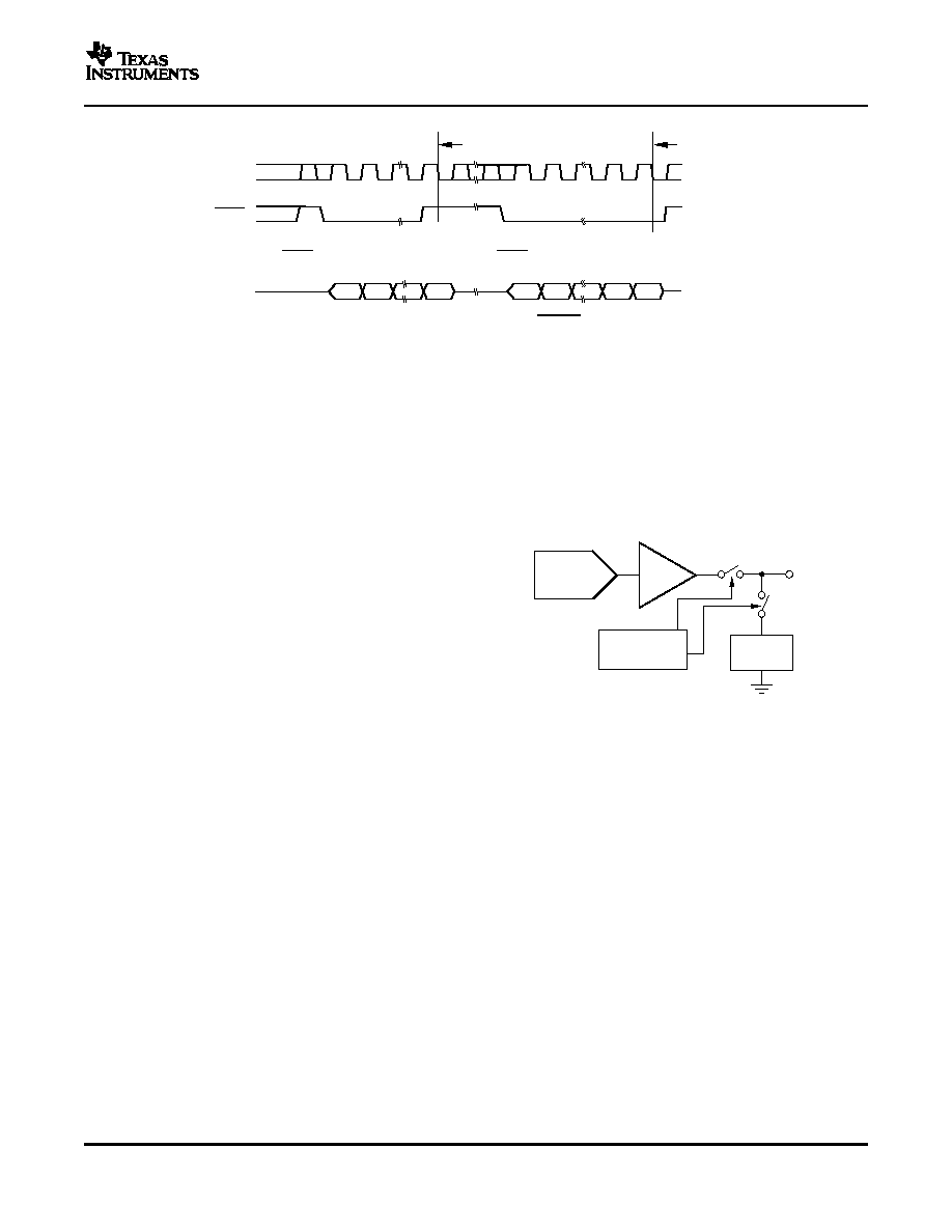
Valid Write-Buffer/DAC Update:
SYNC HIGH After 24th Falling Edge
DB23 DB22
1
2
1
2
DB0
DB23 DB22
DB1
DB0
24th Falling
Edge
24th Falling
Edge
POWER-DOWN MODES
Resistor
String DAC
Amplifier
Power-down
Circuitry
Resistor
Network
V
OUT
X
DAC8554
SLAS431A ≠ JUNE 2005 ≠ REVISED AUGUST 2005
Figure 50. Interrupt and Valid SYNC Timing
Individual channels can separately be powered down,
reducing the total power consumption. When all
channels are powered down, the DAC8554 power
The DAC8554 utilizes four modes of operation. These
consumption drops below 2 µA. There is no power
modes are accessed by setting three bits (PD2, PD1,
-up command. When a channel is updated with data,
and PD0) in the shift register and performing a Load
it automatically exits power-down. All channels exit
action to the DACs. The DAC8554 offers a very
power-down simultaneously after a broadcast data
flexible power-down interface based on channel
update. The time to exit power-down is approximately
register operation. A channel consists of a single
5 µs. See Table 1 and Table 2 for power-down
16-bit DAC with power-down circuitry, a temporary
operation details.
storage register (TR), and a DAC register (DR). TR
and DR are both 18-bit wide. Two MSBs represent
power-down condition and 16 LSBs represent data
for TR and DR. By adding bits 17 and 18 to TR and
DR, a power-down condition can be temporarily
stored and used just like data. Internal circuits ensure
that DB15 and DB14 get transferred to TR17and
TR16 (DR17 and DR16), when DB16 = 1.
The DAC8554 treats the power-down condition like
data and all the operational modes are still valid for
power-down. It is possible to broadcast a power-down
Figure 51. Output Stage During Power-Down
condition to all the DAC8554s in a system, or it is
(High-Impedance)
possible to simultaneously power-down a channel
while updating data on other channels.
DB16, DB15, and DB14 = 100 (or 111) represent a
power-down condition with Hi-Z output impedance for
a selected channel. 101 represents a power-down
condition with 1k output impedance and 110 rep-
resents a power-down condition with 100k output
impedance.
17

www.ti.com
OPERATION EXAMPLES
DAC8554
SLAS431A ≠ JUNE 2005 ≠ REVISED AUGUST 2005
Example 1: Write to data buffer A; through buffer D; load DAC A through DAC D simultaneously
∑
1st -- Write to data buffer A:
A1
A0
LD1
LD0
DC
DAC Sel 1
DAC Sel 0
PD0
DB15
--
DB1
DB0
0
0
0
0
X
0
0
0
D15
--
D1
D0
∑
2nd -- Write to data buffer B:
A1
A0
LD1
LD0
DC
DAC Sel 1
DAC Sel 0
PD0
DB15
--
DB1
DB0
0
0
0
0
X
0
1
0
D15
--
D1
D0
∑
3rd -- Write to data buffer C:
A1
A0
LD1
LD0
DC
DAC Sel 1
DAC Sel 0
PD0
DB15
--
DB1
DB0
0
0
0
0
X
1
0
0
D15
--
D1
D0
∑
4th -- Write to data buffer D and simultaneously update all DACs:
A1
A0
LD1
LD0
DC
DAC Sel 1
DAC Sel 0
PD0
DB15
--
DB1
DB0
0
0
1
0
X
1
1
0
D15
--
D1
D0
The DAC A, DAC B, DAC C, and DAC D analog outputs simultaneously settle to the specified values upon
completion of the 4th write sequence. (The DAC voltages update simultaneously after the 24th SCLK falling edge
of the 4th write cycle).
Example 2: Load New Data to DAC A through DAC D sequentially
∑
1st -- Write to data buffer A and load DAC A: DAC A output settles to specified value upon completion:
A1
A0
LD1
LD0
DC
DAC Sel 1
DAC Sel 0
PD0
DB15
--
DB1
DB0
0
0
0
1
X
0
0
0
D15
--
D1
D0
∑
2nd -- Write to data buffer B and load DAC B: DAC B output settles to specified value upon completion:
A1
A0
LD1
LD0
DC
DAC Sel 1
DAC Sel 0
PD0
DB15
--
DB1
DB0
0
0
0
1
X
0
1
0
D15
--
D1
D0
∑
3rd -- Write to data buffer C and load DAC C: DAC C output settles to specified value upon completion:
A1
A0
LD1
LD0
DC
DAC Sel 1
DAC Sel 0
PD0
DB15
--
DB1
DB0
0
0
0
1
X
1
0
0
D15
--
D1
D0
∑
4th -- Write to data buffer D and load DAC D: DAC D output settles to specified value upon completion:
A1
A0
LD1
LD0
DC
DAC Sel 1
DAC Sel 0
PD0
DB15
--
DB1
DB0
0
0
0
1
X
1
1
0
D15
--
D1
D0
After completion of each write cycle, DAC analog output settles to the voltage specified.
Example 3: Power-down DAC A and DAC B to 1 k
and Power-down DAC C and DAC D to 100 k
simultaneously
∑
Write power-down command to data buffer A: DAC A to 1 k
.
A1
A0
LD1
LD0
DC
DAC Sel 1
DAC Sel 0
PD0
DB15
DB14
DB13
--
0
0
0
0
X
0
0
1
0
1
X
--
∑
Write power-down command to data buffer B: DAC B to 1 k
.
A1
A0
LD1
LD0
DC
DAC Sel 1
DAC Sel 0
PD0
DB15
DB14
DB13
--
0
0
0
0
X
0
1
1
0
1
X
--
∑
Write power-down command to data buffer C: DAC C to 1 k
.
A1
A0
LD1
LD0
DC
DAC Sel 1
DAC Sel 0
PD0
DB15
DB14
DB13
--
0
0
0
0
X
1
0
1
1
0
X
--
18

www.ti.com
ENABLE PIN
LDAC FUNCTIONALITY
MICROPROCESSOR INTERFACING
DAC8554 TO 8051 Interface
DAC8554
SLAS431A ≠ JUNE 2005 ≠ REVISED AUGUST 2005
∑
Write power-down command to data buffer D: DAC D to 100 k
and simultaneously update all DACs.
A1
A0
LD1
LD0
DC
DAC Sel 1
DAC Sel 0
PD0
DB15
DB14
DB13
--
0
0
1
0
X
1
1
1
1
0
X
--
The DAC A, DAC B, DAC C, and DAC D analog outputs simultaneously power-down to each respective specified
mode upon completion of the 4th write sequence.
Example 4: Power-Down DAC A Through DAC D to High-Impedance Sequentially:
∑
Write power-down command to data buffer A and load DAC A: DAC A output = Hi-Z:
A1
A0
LD1
LD0
DC
DAC Sel 1
DAC Sel 0
PD0
DB15
DB14
DB13
--
0
0
0
1
X
0
0
1
1
1
X
--
∑
Write power-down command to data buffer B and load DAC B: DAC B output = Hi-Z:
A1
A0
LD1
LD0
DC
DAC Sel 1
DAC Sel 0
PD0
DB15
DB14
DB13
--
0
0
0
1
X
0
1
1
1
1
x
--
∑
Write power-down command to data buffer C and load DAC C: DAC C output = Hi-Z:
A1
A0
LD1
LD0
DC
DAC Sel 1
DAC Sel 0
PD0
DB15
DB14
DB13
--
0
0
0
1
X
1
0
1
1
1
X
--
∑
Write power-down command to data buffer D and load DAC D: DAC D output = Hi-Z:
A1
A0
LD1
LD0
DC
DAC Sel 1
DAC Sel 0
PD0
DB15
DB14
DB13
--
0
0
0
1
X
1
1
1
1
1
X
--
The DAC A, DAC B, DAC C, and DAC D analog
outputs sequentially power-down to high-impedance
upon completion of the 1st, 2nd, 3rd, and 4th write
For normal operation, the enable pin must be tied to
sequences, respectively.
a logic low. If the enable pin is tied high, the
DAC8554 stops listening to the serial port. This can
be useful for applications that share the same serial
The DAC8554 offers both a software and hardware
port.
simultaneous
update
function.
The
DAC8554
double-buffered architecture has been designed so
that new data can be entered for each DAC without
disturbing the analog outputs. The software simul-
taneous update capability is controlled by the load 1
See
Figure 52
for a serial interface between the
(LD1) and load 0 (LD0) control bits. By setting load 1
DAC8554 and a typical 8051-type micro controller.
equal to 1 all of the DAC registers will be updated on
The setup for the interface is as follows: TXD of the
the falling edge of the 24th clock signal. When the
8051 drives SCLK of the DAC8554, while RXD drives
new data has been entered into the device, all of the
the serial data line of the device. The SYNC signal is
DAC outputs can be updated simultaneously and
derived from a bit-programmable pin on the port of
synchronously with the clock.
the 8051. In this case, port line P3.3 is used. When
DAC8554 data updates are synchronized with the
data is to be transmitted to the DAC8554, P3.3 is
falling edge of the 24th SCLK cycle, which follows a
taken LOW. The 8051 transmits data in 8-bit bytes;
falling edge of SYNC. For such synchronous updates,
thus only eight falling clock edges occur in the
the LDAC pin is not required and it must be connec-
transmit cycle. To load data to the DAC, P3.3 is left
ted to GND permanently. The LDAC pin is used as a
LOW after the first eight bits are transmitted, then a
positive edge triggered timing signal for asynchro-
second and third write cycle is initiated to transmit the
nous DAC updates. Data buffers of all channels must
remaining data. P3.3 is taken HIGH following the
be loaded with desired data before LDAC is triggered.
completion of the third write cycle. The 8051 outputs
After a low-to-high LDAC transition, all DACs are
the serial data in a format which presents the LSB
simultaneously updated with the contents of their
first, while the DAC8554 requires its data with the
corresponding data buffers. If the content of a data
MSB as the first bit received. The 8051 transmit
buffer is not changed by the serial interface, the
routine must therefore take this into account, and
corresponding DAC output will remain unchanged
mirror the data as needed.
after the LDAC trigger.
19
www.ti.com
80C51/80L51
(1)
P3.3
TXD
RXD
SYNC
SCLK
D
IN
(1) Additional pins omitted for clarity.
DAC8554
DAC8554 to Microwire Interface
DAC8554 to TMS320 DSP Interface
SYNC
SCLK
D
IN
Microwire
TM
CS
SK
SO
(1) Additional pins omitted for clarity.
Microwire is a registered trademark of National Semiconductor.
DAC8554
DAC8554 to 68HC11 Interface
DAC8554
TMS320 DSP
SYNC
D
IN
SCLK
FSX
DX
CLKX
AV
DD
V
OUT
A
V
OUT
D
Output A
Output D
Reference
Input
V
REF
L
V
REF
H
GND
0.1
F
1
F to 10
F
Positive Supply
0.1
F
10
F
68HC11
(1)
PC7
SCK
MOSI
SYNC
SCLK
D
IN
(1) Additional pins omitted for clarity.
DAC8554
DAC8554
SLAS431A ≠ JUNE 2005 ≠ REVISED AUGUST 2005
causes data appearing on the MOSI output to be
valid on the falling edge of SCLK. When data is being
transmitted to the DAC, the SYNC line is held LOW
(PC7). Serial data from the 68HC11 is transmitted in
8-bit bytes with only eight falling clock edges
occurring in the transmit cycle. (Data is transmitted
MSB first.) In order to load data to the DAC8554,
PC7 is left LOW after the first eight bits are trans-
ferred, then a second and third serial write operation
Figure 52. DAC8554 to 80C51/80L51 Interface
is performed to the DAC. PC7 is taken HIGH at the
end of this procedure.
Figure 53
shows an interface between the DAC8554
Figure 55
shows the connections between the
and any Microwire compatible device. Serial data is
DAC8554 and a TMS320 Digital Signal Processor
shifted out on the falling edge of the serial clock and
(DSP). A Single DSP can control up to four
is clocked into the DAC8554 on the rising edge of the
DAC8554s without any interface logic.
CK signal.
Figure 53. DAC8554 to Microwire Interface
Figure 54
shows a serial interface between the
DAC8554 and the 68HC11 micro controller. SCK of
Figure 55. DAC8554 to TMS320 DSP
the 68HC11 drives the SCLK of the DAC8554, while
the MOSI output drives the serial data line of the
DAC. The SYNC signal is derived from a port line
(PC7), similar to the 8051 diagram.
Figure 54. DAC8554 to 68HC11 Interface
The 68HC11 should be configured so that its CPOL
bit is 0 and its CPHA bit is 1. This configuration
20

www.ti.com
APPLICATION INFORMATION
CURRENT CONSUMPTION
OUTPUT VOLTAGE STABILITY
DRIVING RESISTIVE AND CAPACITIVE
SETTLING TIME AND OUTPUT GLITCH PER-
DIFFERENTIAL AND INTERGRAL
CROSSTALK AND AC PERFORMANCE
USING THE REF02 AS A POWER SUPPLY
DAC8554
SLAS431A ≠ JUNE 2005 ≠ REVISED AUGUST 2005
The DAC8554 consumes a maximum of 250 µA at
The DAC8554 exhibits excellent temperature stability
AV
DD
= 5 V and 240 µA at AV
DD
= 3 V for each active
of 5 ppm/
∞
C typical output voltage drift over the
channel, including reference current consumption.
specified temperature range of the device. This en-
Additional current consumption can occur at the
ables the output voltage of each channel to stay
digital inputs if V
IH
<< IOV
DD
. For most efficient power
within a
±
25 µV window for a
±
1
∞
C ambient tempera-
operation, CMOS logic levels are recommended at
ture change.
the digital inputs to the DAC.
Good power-supply rejection ratio (PSRR) perform-
In power-down mode, typical current consumption is
ance reduces supply noise present on AV
DD
from
200 nA per channel. A delay time of 10 ms to 20 ms
appearing at the outputs to well below 10 µV-s.
after a power-down command is issued to the DAC is
Combined with good dc noise performance and true
typically sufficient for the power-down current to drop
16-bit differential linearity, the DAC8554 becomes a
below 10 µA.
perfect choice for closed-loop control applications.
LOADS
FORMANCE
The DAC8554 output stage is capable of driving
DAC8554 settles to ±0.003% of its full-scale range
loads of up to 1000 pF while remaining stable. Within
within 10 µs, driving a 200 pF 2 K
load. For good
the offset and gain error margins, the DAC8554 can
settling performance the outputs should not approach
operate rail-to-rail when driving a capacitive load.
the top and bottom rails. Small signal settling time is
Resistive loads of 2 k
can be driven by the
under 1 µs, enabling data update rates exceeding 1
DAC8554 while achieving good load regulation.
MSPS for small code changes.
When the outputs of the DAC are driven to the
Many applications are sensitive to undesired transient
positive rail under resistive loading, the PMOS tran-
signals such as glitch. DAC8554 has a proprietary,
sistor of each Class-AB output stage can enter into
ultra-low glitch architecture addressing such appli-
the linear region. When this occurs, the added IR
cations. Code-to-code glitches rarely exceed millivolt
voltage drop deteriorates the linearity performance of
and they last under 0.3 µs. Typical glitch energy is an
the DAC. This only occurs within approximately the
outstanding 0.15 nV-s. Theoretical worst cast glitch
top 100 mV of the DAC's output voltage character-
should occur during a 256 LSB step, but it is so low, it
istic. Under resistive loading conditions, good linearity
cannot be detected.
is preserved as long as the output voltage is at least
100 mV below the AVDD voltage.
NONLINEARITY
DAC8554 uses precision thin film resistors to achieve
The DAC8554 architecture uses separate resistor
monotonicity and good linearity. Typical linearity error
strings for each DAC channel in order to achieve
is
±
4 LSBs;
±
0.3 mV error for a 5 V range. Differential
ultra-low crosstalk performance. DC crosstalk seen at
linearity is typically
±
0.25 LSBs,
±
19 µV error for a
one channel during a full-scale change on the
consecutive code change.
neighboring channel is typically less than 0.5LSBs.
The AC crosstalk measured (for a full-scale, 1 kHz
sine wave output generated at one channel, and
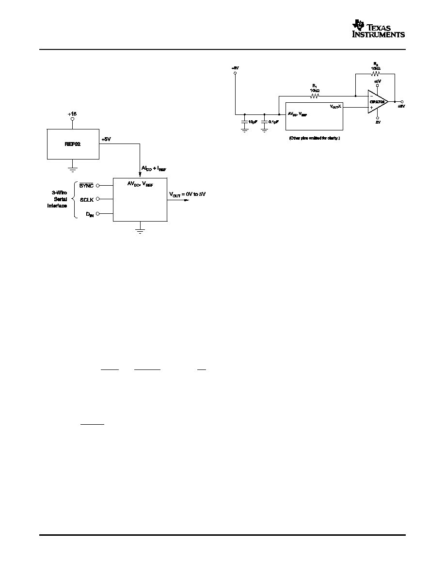
FOR THE DAC8554
measured at the remaining output channel) is typi-
cally under ≠100 dB.
Due to the extremely low supply current required by
the DAC8554, a possible configuration is to use a
In addition, the DAC8554 can achieve typical AC
REF02 +5 V precision voltage reference to supply the
performance of 96 dB signal-to-noise ratio (SNR) and
required voltage to the DAC8554s supply input as
85 dB total harmonic distortion (THD), making the
well as the reference input, as shown in
Figure 56
.
DAC8554 a solid choice for applications requiring
This is especially useful if the power supply is quite
high SNR at output frequencies at or below 10 kHz.
noisy or if the system supply voltages are at some
value other than 5 V. The REF02 will output a steady
supply voltage for the DAC8554. If the REF02 is
21
www.ti.com
-
DAC8554
LAYOUT
DAC8554
BIPOLAR OPERATION USING THE DAC8554
V
OUT
X
+
V
ref
D
65536
R1
)
R2
R1
*
V
ref
R2
R1
V
OUT
X
*
+
10
D
65536
)
5 V
DAC8554
SLAS431A ≠ JUNE 2005 ≠ REVISED AUGUST 2005
used, the current it needs to supply to the DAC8554
is 0.85 mA typical for AV
DD
= 5 V. When a DAC
output is loaded, the REF02 also needs to supply the
current to the load. The total typical current required
(with a 5 k
load on a given DAC output) is:
0.85 mA + (5V/5 k
) = 1.085 mA
Figure 57. Bipolar Operation With the DAC8554
A precision analog component requires careful layout,
adequate bypassing, and clean, well-regulated power
supplies.
The DAC8554 offers single-supply operation, and it
will often be used in close proximity with digital logic,
micro controllers, microprocessors, and digital signal
processors. The more digital logic present in the
Figure 56. REF02 as a Power Supply to the
design and the higher the switching speed, the more
DAC8554
difficult it will be to keep digital noise from appearing
at the output.
Due to the single ground pin of the DAC8554, all
return currents, including digital and analog return
The DAC8554 has been designed for single-supply
currents for the DAC, must flow through a single
operation, but a bipolar output range is also possible
point. Ideally, GND would be connected directly to an
using the circuit in
Figure 57
. The circuit shown will
analog ground plane. This plane would be separate
give an output voltage range of
±
V
ref
. Rail-to-rail
from
the
ground
connection
for
the
digital
operation at the amplifier output is achievable using
components
until
they
were
connected
at
the
an amplifier such as the OPA703, as shown in
power-entry point of the system.
REF
Figure 57
.
The power applied to AV
DD
should be well regulated
The output voltage for any input code can be calcu-
and low noise. Switching power supplies and DC/DC
lated as follows:
converters will often have high-frequency glitches or
spikes riding on the output voltage. In addition, digital
components can create similar high-frequency spikes
as their internal logic switches states. This noise can
where D represents the input code in decimal
easily couple into the DAC output voltage through
(0≠65535).
various paths between the power connections and
analog output.
With V
ref
= 5 V, R1 = R2 = 10 k
.
As with the GND connection, AV
DD
should be con-
nected to a positive power-supply plane or trace that
is separate from the connection for digital logic until
This is an output voltage range of
±
5 V with 0000
H
they are connected at the power-entry point. In
corresponding to a ≠5 V output and FFFF
H
corre-
addition, a 1 µF to 10 µF capacitor in parallel with a
sponding to a 5 V output. Similarly, using V
ref
= 2.5 V
0.1 µF bypass capacitor is strongly recommended. In
a
±
2.5 V output voltage range can be achieved.
some situations, additional bypassing may be re-
quired, such as a 100 µF electrolytic capacitor or
even a Pi filter made up of inductors and capacitors ≠
all designed to essentially low-pass filter the supply,
removing the high-frequency noise.
22

www.ti.com
DAC8554
SLAS431A ≠ JUNE 2005 ≠ REVISED AUGUST 2005
Up to four DAC8554 devices can be used on a single
PCBs. Therefore, if the digital signal rise time is 1 ns,
SPI bus without any glue logic to create a high
the distance between any two DAC8554s have to be
channel count solution. Special attention is required
further apart on the PCB, the signal rise times should
to avoid digital signal integrity problems when using
be reduced by placing series resistors at the drivers
multiple DAC8554s on the same SPI bus. Signal
for SYNC, SCLK, and D
IN
lines. If the largest distance
integrity of SYNC, SCLK, and D
IN
lines will not be an
between any two DAC8554s must to be six inches,
issue as long as the rise times of these digital signals
the rise time should be reduced to 6 ns with an RC
are longer than six times the propagation delay
network formed by the series resistor at the digital
between any two DAC8554 devices. Propagation
driver and the total trace and input capacitance on
speed is approximately six inches/ns on standard
the PCB.
23
PACKAGING INFORMATION
Orderable Device
Status
(1)
Package
Type
Package
Drawing
Pins Package
Qty
Eco Plan
(2)
Lead/Ball Finish
MSL Peak Temp
(3)
DAC8554IPW
ACTIVE
TSSOP
PW
16
90
Green (RoHS &
no Sb/Br)
CU NIPDAU
Level-1-260C-UNLIM
DAC8554IPWG4
ACTIVE
TSSOP
PW
16
90
Green (RoHS &
no Sb/Br)
CU NIPDAU
Level-1-260C-UNLIM
DAC8554IPWR
ACTIVE
TSSOP
PW
16
2000 Green (RoHS &
no Sb/Br)
CU NIPDAU
Level-1-260C-UNLIM
DAC8554IPWRG4
ACTIVE
TSSOP
PW
16
2000 Green (RoHS &
no Sb/Br)
CU NIPDAU
Level-1-260C-UNLIM
(1)
The marketing status values are defined as follows:
ACTIVE: Product device recommended for new designs.
LIFEBUY: TI has announced that the device will be discontinued, and a lifetime-buy period is in effect.
NRND: Not recommended for new designs. Device is in production to support existing customers, but TI does not recommend using this part in
a new design.
PREVIEW: Device has been announced but is not in production. Samples may or may not be available.
OBSOLETE: TI has discontinued the production of the device.
(2)
Eco
Plan
-
The
planned
eco-friendly
classification:
Pb-Free
(RoHS)
or
Green
(RoHS
&
no
Sb/Br)
-
please
check
http://www.ti.com/productcontent
for the latest availability information and additional product content details.
TBD: The Pb-Free/Green conversion plan has not been defined.
Pb-Free (RoHS): TI's terms "Lead-Free" or "Pb-Free" mean semiconductor products that are compatible with the current RoHS requirements
for all 6 substances, including the requirement that lead not exceed 0.1% by weight in homogeneous materials. Where designed to be soldered
at high temperatures, TI Pb-Free products are suitable for use in specified lead-free processes.
Green (RoHS & no Sb/Br): TI defines "Green" to mean Pb-Free (RoHS compatible), and free of Bromine (Br) and Antimony (Sb) based flame
retardants (Br or Sb do not exceed 0.1% by weight in homogeneous material)
(3)
MSL, Peak Temp. -- The Moisture Sensitivity Level rating according to the JEDEC industry standard classifications, and peak solder
temperature.
Important Information and Disclaimer:The information provided on this page represents TI's knowledge and belief as of the date that it is
provided. TI bases its knowledge and belief on information provided by third parties, and makes no representation or warranty as to the
accuracy of such information. Efforts are underway to better integrate information from third parties. TI has taken and continues to take
reasonable steps to provide representative and accurate information but may not have conducted destructive testing or chemical analysis on
incoming materials and chemicals. TI and TI suppliers consider certain information to be proprietary, and thus CAS numbers and other limited
information may not be available for release.
In no event shall TI's liability arising out of such information exceed the total purchase price of the TI part(s) at issue in this document sold by TI
to Customer on an annual basis.
PACKAGE OPTION ADDENDUM
www.ti.com
13-Sep-2005
Addendum-Page 1
MECHANICAL DATA
MTSS001C ≠ JANUARY 1995 ≠ REVISED FEBRUARY 1999
POST OFFICE BOX 655303
∑
DALLAS, TEXAS 75265
PW (R-PDSO-G**)
PLASTIC SMALL-OUTLINE PACKAGE
14 PINS SHOWN
0,65
M
0,10
0,10
0,25
0,50
0,75
0,15 NOM
Gage Plane
28
9,80
9,60
24
7,90
7,70
20
16
6,60
6,40
4040064/F 01/97
0,30
6,60
6,20
8
0,19
4,30
4,50
7
0,15
14
A
1
1,20 MAX
14
5,10
4,90
8
3,10
2,90
A MAX
A MIN
DIM
PINS **
0,05
4,90
5,10
Seating Plane
0
∞
≠ 8
∞
NOTES: A. All linear dimensions are in millimeters.
B. This drawing is subject to change without notice.
C. Body dimensions do not include mold flash or protrusion not to exceed 0,15.
D. Falls within JEDEC MO-153

IMPORTANT NOTICE
Texas Instruments Incorporated and its subsidiaries (TI) reserve the right to make corrections, modifications,
enhancements, improvements, and other changes to its products and services at any time and to discontinue
any product or service without notice. Customers should obtain the latest relevant information before placing
orders and should verify that such information is current and complete. All products are sold subject to TI's terms
and conditions of sale supplied at the time of order acknowledgment.
TI warrants performance of its hardware products to the specifications applicable at the time of sale in
accordance with TI's standard warranty. Testing and other quality control techniques are used to the extent TI
deems necessary to support this warranty. Except where mandated by government requirements, testing of all
parameters of each product is not necessarily performed.
TI assumes no liability for applications assistance or customer product design. Customers are responsible for
their products and applications using TI components. To minimize the risks associated with customer products
and applications, customers should provide adequate design and operating safeguards.
TI does not warrant or represent that any license, either express or implied, is granted under any TI patent right,
copyright, mask work right, or other TI intellectual property right relating to any combination, machine, or process
in which TI products or services are used. Information published by TI regarding third-party products or services
does not constitute a license from TI to use such products or services or a warranty or endorsement thereof.
Use of such information may require a license from a third party under the patents or other intellectual property
of the third party, or a license from TI under the patents or other intellectual property of TI.
Reproduction of information in TI data books or data sheets is permissible only if reproduction is without
alteration and is accompanied by all associated warranties, conditions, limitations, and notices. Reproduction
of this information with alteration is an unfair and deceptive business practice. TI is not responsible or liable for
such altered documentation.
Resale of TI products or services with statements different from or beyond the parameters stated by TI for that
product or service voids all express and any implied warranties for the associated TI product or service and
is an unfair and deceptive business practice. TI is not responsible or liable for any such statements.
Following are URLs where you can obtain information on other Texas Instruments products and application
solutions:
Products
Applications
Amplifiers
amplifier.ti.com
Audio
www.ti.com/audio
Data Converters
dataconverter.ti.com
Automotive
www.ti.com/automotive
DSP
dsp.ti.com
Broadband
www.ti.com/broadband
Interface
interface.ti.com
Digital Control
www.ti.com/digitalcontrol
Logic
logic.ti.com
Military
www.ti.com/military
Power Mgmt
power.ti.com
Optical Networking
www.ti.com/opticalnetwork
Microcontrollers
microcontroller.ti.com
Security
www.ti.com/security
Telephony
www.ti.com/telephony
Video & Imaging
www.ti.com/video
Wireless
www.ti.com/wireless
Mailing Address:
Texas Instruments
Post Office Box 655303 Dallas, Texas 75265
Copyright
2005, Texas Instruments Incorporated