 | –≠–ª–µ–∫—Ç—Ä–æ–Ω–Ω—ã–π –∫–æ–º–ø–æ–Ω–µ–Ω—Ç: DAC8831ID | –°–∫–∞—á–∞—Ç—å:  PDF PDF  ZIP ZIP |

Burr Brown Products
from Texas Instruments
FEATURES
DESCRIPTION
APPLICATIONS
DAC
DAC8830
SDI
SCLK
CS
V
REF
DGND
V
OUT
AGND
S
e
r
i
a
l
I
n
t
e
r
f
a
c
e
Input
Register
DAC Latch
RFB
INV
AGNDF
AGNDS
DGND
DAC
DAC Latch
Input
Register
DAC8831
DAC8831
Functional Block Diagram
DAC8830
Functional Block Diagram
+
-
+V
-
V
OPA277
OPA704
OPA727
SDI
SCLK
LDAC
V
OUT
V
O
V
DD
R
FB
R
INV
V
REF
-
F
V
REF
-
S
S
e
r
i
a
l
I
n
t
e
r
f
a
c
e
a
n
d
C
o
n
t
r
o
l
L
o
g
i
c
V
DD
CS
DAC8830
DAC8831
SLAS449A ≠ FEBRUARY 2005 ≠ REVISED MARCH 2005
16-Bit, Ultra-Low Power, Voltage-Output
Digital-to-Analog Converters
∑
16-Bit Resolution
The DAC8830 and DAC8831 are single, 16-bit,
serial-input,
voltage-output
digital-to-analog
con-
∑
2.7V to 5.5V Single-Supply Operation
verters (DACs) operating from a single 3V to 5V
∑
Very Low Power: 15µW for 3V Power
power supply. These converters provide excellent
∑
High Accuracy, INL: 1LSB
linearity (1LSB INL), low glitch, low noise, and fast
∑
Low Glitch: 8nV-s
settling (1.0µS to 1/2 LSB of full-scale output) over
the specified temperature range of ≠40
∞
C to +85
∞
C.
∑
Low Noise: 10nV/
Hz
The output is unbuffered, which reduces the power
∑
Fast Settling: 1.0µS
consumption and the error introduced by the buffer.
∑
Fast SPI Interface, up to 50MHz
These parts feature a standard high-speed (clock up
∑
Reset to Zero-Code
to 50MHz), 3V or 5V SPI serial interface to communi-
∑
Schmitt-Trigger Inputs for Direct Optocoupler
cate with the DSP or microprocessors.
Interface
The DAC8830 output is 0V to V
REF
. However, the
∑
Industry-Standard Pin Configuration
DAC8831 provides bipolar output (
±
V
REF
) when work-
ing with an external buffer. The DAC8830 and
DAC8831 are both reset to zero-code after power up.
∑
Portable Equipment
For optimum performance, a set of Kelvin connec-
∑
Automatic Test Equipment
tions to external reference and analog ground input
are provided on the DAC8831.
∑
Industrial Process Control
∑
Data Acquisition Systems
The DAC8830 is available in an SO-8 package and
the DAC8831 in an SO-14 package. Both have
∑
Optical Networking
industry standard pinouts (see Table 3, the Cross
Reference table in the Application Information section
for details).
Please be aware that an important notice concerning availability, standard warranty, and use in critical applications of Texas
Instruments semiconductor products and disclaimers thereto appears at the end of this data sheet.
All trademarks are the property of their respective owners.
PRODUCTION DATA information is current as of publication date.
Copyright © 2005, Texas Instruments Incorporated
Products conform to specifications per the terms of the Texas
Instruments standard warranty. Production processing does not
necessarily include testing of all parameters.

www.ti.com
ABSOLUTE MAXIMUM RATINGS
DAC8830
DAC8831
SLAS449A ≠ FEBRUARY 2005 ≠ REVISED MARCH 2005
This integrated circuit can be damaged by ESD. Texas Instruments recommends that all integrated
circuits be handled with appropriate precautions. Failure to observe proper handling and installation
procedures can cause damage.
ESD damage can range from subtle performance degradation to complete device failure. Precision
integrated circuits may be more susceptible to damage because very small parametric changes could
cause the device not to meet its published specifications.
ORDERING INFORMATION
(1)
MINIMUM
POWER-
RELATIVE
DIFFERENTIAL
ON
SPECIFICATION
TRANSPORT
ACCURACY
NONLINEARITY
RESET
TEMPERATURE
PACKAGE
PACKAGE-
PACKAGE
ORDERING
MEDIA,
PRODUCT
(LSB)
(LSB)
VALUE
RANGE
MARKING
LEAD
DESIGNATOR
NUMBER
QUANTITY
DAC8830IDT
Tape and Reel, 250
DAC8830ID
±
4
±
1
Zero-Code
≠40
∞
C to 85
∞
C
8830I
SO-8
D
DAC8830IDR
Tape and Reel, 2500
DAC8830IBDT
Tape and Reel, 250
DAC8830IBD
±
2
±
1
Zero-Code
≠40
∞
C to 85
∞
C
8830I
SO-8
D
DAC8830IBDR
Tape and Reel, 2500
DAC8830ICDT
Tape and Reel, 250
DAC8830ICD
±
1
±
1
Zero-Code
≠40
∞
C to 85
∞
C
8830I
SO-8
D
DAC8830ICDR
Tape and Reel, 2500
DAC8831ID
Tube, 58
DAC8831ID
±
4
±
1
Zero-Code
≠40
∞
C to 85
∞
C
8831I
SO-14
D
DAC8831IDR
Tape and Reel, 2500
DAC8831IBD
Tube, 58
DAC8831IBD
±
2
±
1
Zero-Code
≠40
∞
C to 85
∞
C
8831I
SO-14
D
DAC8831IBDR
Tape and Reel, 2500
DAC8831ICD
Tube, 58
DAC8831ICD
±
1
±
1
Zero-Code
≠40
∞
C to 85
∞
C
8831I
SO-14
D
DAC8831ICDR
Tape and Reel, 2500
(1)
For the most current package and ordering information, see the Package Option Addendum at the end of this data sheet, or see the TI
website at www.ti.com.
over operating free-air temperature range (unless otherwise noted)
(1)
DAC8830, DAC8831
UNIT
V
DD
to AGND
≠0.3 to +7
V
Digital input voltage to DGND
≠0.3 to +V
DD
+ 0.3
V
V
OUT
to AGND
≠0.3 to +V
DD
+ 0.3
V
AGND, AGNDF, AGNDS to DGND
≠0.3 to +0.3
V
Operating temperature range
≠40 to +85
∞
C
Storage temperature range
≠65 to +150
∞
C
Junction temperature range (T
J
max)
+150
∞
C
Power dissipation
(T
J
max - T
A
) /
JA
W
SO-8
149.5
∞
C/W
Thermal impedance,
JA
SO-14
104.5
∞
C/W
Vapor phase (60s)
+215
∞
C
Lead temperature, soldering
Infrared (15s)
+220
∞
C
(1)
Stresses above those listed under absolute maximum ratings may cause permanent damage to the device. Exposure to absolute
maximum conditions for extended periods may affect device reliability.
2

www.ti.com
ELECTRICAL CHARACTERISTICS
DAC8830
DAC8831
SLAS449A ≠ FEBRUARY 2005 ≠ REVISED MARCH 2005
All specifications at T
A
= T
MIN
to T
MAX
, V
DD
= 3V, or V
DD
= 5V, V
REF
= 2.5V unless otherwise noted; specifications subject to
change without notice.
PARAMETER
CONDITIONS
MIN
TYP
MAX
UNIT
STATIC PERFORMANCE
Resolution
16
bits
DAC8830ICD, DAC8831ICD,
±
0.5
±
1
Linearity error
DAC8830IBD, DAC8831IBD
±
0.5
±
2
LSB
DAC8830ID, DAC8831ID
±
0.5
±
4
Differential linearity error
All grades
±
0.5
±
1
LSB
T
A
= +25
∞
C
±
1
±
5
Gain error
LSB
T
A
= ≠40
∞
C to +85
∞
C
±
7
Gain drift
±
0.1
ppm/
∞
C
T
A
= +25
∞
C
±
0.25
±
1
Zero code error
LSB
T
A
= ≠40
∞
C to +85
∞
C
±
2
Zero code drift
±
0.05
ppm/
∞
C
OUTPUT CHARACTERISTICS
Unipolar operation
0
+V
REF
V
Voltage output
(1)
(DAC8831 only)
Bipolar operation
≠V
REF
+V
REF
V
Output Impedance
6.25
k
Settling time
To 1/2 LSB of FS, C
L
= 10pF
1
µs
Slew rate
(2)
C
L
= 10pF
25
V/µs
1LSB change around major
Digital-to-analog glitch
8
nV-s
carry
Digital feedthrough
(3)
0.2
nV-s
DAC8830
10
Output noise
T
A
= +25
∞
C
nV/
Hz
DAC8831
18
Power supply rejection
V
DD
varies
±
10%
±
1
LSB
R
FB
/ R
INV
1
/
Bipolar resistor
DAC8831 only
matching
Ratio error
±
0.0015
±
0.0076
%
T
A
= +25
∞
C
±
0.25
±
5
Bipolar zero error
DAC8831 only
LSB
T
A
= ≠40
∞
C to +85
∞
C
±
7
Bipolar zero drift
DAC8831 only
±
0.2
ppm/
∞
C
(1)
TheDAC8830 output is unipolar (0V to +V
REF
). TheDAC8831 output is bipolar (
±
V
REF
) when it connects to an external buffer (see the
Bipolar Output Operation section for details).
(2)
Slew Rate is measure from 10% to 90% of transition when the output changes from 0 to full scale.
(3)
Digital feedthrough is defined as the impulse injected into the analog output from the digital input. It is measured when the DAC output
does not change, CS is held high, while SCLK and DIN signals are toggled.
3

www.ti.com
DAC8830
DAC8831
SLAS449A ≠ FEBRUARY 2005 ≠ REVISED MARCH 2005
ELECTRICAL CHARACTERISTICS (continued)
All specifications at T
A
= T
MIN
to T
MAX
, V
DD
= 3V, or V
DD
= 5V, V
REF
= 2.5V unless otherwise noted; specifications subject to
change without notice.
PARAMETER
CONDITIONS
MIN
TYP
MAX
UNIT
REFERENCE INPUT
Reference input voltage range
1.25
V
DD
V
Unipolar mode
9
Reference input impedance
(4)
k
Bipolar mode, DAC8831
7.5
Reference ≠3dB bandwidth, BW
Code = FFFFh
1.3
MHz
Code = 0000h, V
REF
= 1 V
PP
at
Reference feedthrough
1
mV
100kHz
Signal-to-noise ratio, SNR
92
dB
Code = 0000h
75
Reference input capacitance
pF
Code = FFFFh
120
DIGITAL INPUTS
V
DD
= 2.7V
0.6
V
IL
Input low voltage
V
V
DD
= 5V
0.8
V
DD
= 2.7V
2.1
V
IH
Input high voltage
V
V
DD
= 5V
2.4
Input current
±
1
µA
Input capacitance
10
pF
Hysteresis voltage
0.4
V
POWER SUPPLY
V
DD
2.7
5.5
V
V
DD
= 3V
5
20
I
DD
µA
V
DD
= 5V
5
20
V
DD
= 3V
15
60
Power
µW
V
DD
= 5V
25
100
TEMPERATURE RANGE
Specified performance
≠40
+85
∞
C
(4)
Reference input resistance is code-dependent, minimum at 8555h.
4

www.ti.com
PIN CONFIGURATION (NOT TO SCALE)
1
2
3
4
8
7
6
5
V
OUT
AGND
V
REF
CS
V
DD
DGND
SDI
SCLK
DAC8830
1
2
3
4
5
6
7
14
13
12
11
10
9
8
RFB
V
OUT
AGNDF
AGNDS
V
REF
-S
V
REF
-F
CS
V
DD
INV
DGND
LDAC
SDI
NC
SCLK
NC - No internal connection
DAC8831
DAC8830
DAC8831
SLAS449A ≠ FEBRUARY 2005 ≠ REVISED MARCH 2005
DAC8830ID, DAC8830IBD,
DAC8831ID, DAC8831IBD,
DAC8830ICD (SO-8)
DAC8831ICD (SO-14)
(TOP VIEW)
(TOP VIEW)
TERMINAL FUNCTIONS
TERMINAL
DESCRIPTION
NO.
NAME
DAC8830
1
V
OUT
Analog output of DAC
2
AGND
Analog ground
3
V
REF
Voltage reference input
4
CS
Chip select input (active low). Data is not clocked into SDI unless CS is low
5
SCLK
Serial clock input
6
SDI
Serial data input. Data is latched into input register on the rising edge of SCLK.
7
DGND
Digital ground
8
VDD
Analog power supply, 3V to 5V
DAC8831
1
RFB
Feedback resistor. Connect to the output of external operational amplifier in bipolar mode.
2
V
OUT
Analog output of DAC
3
AGNDF
Analog ground (Force)
4
AGNDS
Analog ground (Sense)
5
V
REF-
S
Voltage reference input (Sense). Connect to external voltage reference
6
V
REF-
F
Voltage reference input (Force). Connect to external voltage reference
7
CS
Chip select input (active low). Data is not clocked into SDI unless CS is low.
8
SCLK
Serial clock input.
9
NC
No internal connection
10
SDI
Serial data input. Data is latched into input register on the rising edge of SCLK.
Load DAC control input. Active low. When LDAC is Low, the DAC latch is simultaneously updated with the content
11
LDAC
of the input register.
12
DGND
Digital ground
Junction point of internal scaling resistors. Connect to external operational amplifier's inverting input in bipolar
13
INV
mode.
14
VDD
Analog power supply, 3V to 5V.
5

www.ti.com
° ° ° °
° ° ° °
° ° ° °
° ° ° °
BIT-14
BIT-13, . . . ,1
BIT-15 (MSB)
BIT-0
DAC
Updated
° °
° °
° ° ° °
-- Don't Care
° °
° °
t
Delay
t
Lead
t
wsck
t
td
t
wsck
t
Lag
t
DSCLK
t
su
t
ho
CS
SCLK
SDI
t
sck
° ° ° °
° ° ° °
° ° °
° ° °
BIT-14
BIT-13, . . . ,1
BIT-15 (MSB)
BIT-0
DAC
Updated
° ° °
° ° °
° ° ° °
° ° ° °
-- Don't Care
° °
° °
t
Delay
t
Lead
t
wsck
t
td
t
wsck
t
Lag
t
DSCLK
t
su
t
ho
CS
SCLK
SDI
LOW
LDAC
° ° ° °
° ° ° °
° ° °
° ° °
BIT-14
BIT-13, . . . ,1
BIT-15 (MSB)
BIT-0
DAC
Updated
° ° °
° ° °
° ° ° °
-- Don't Care
° °
° °
t
Delay
t
Lead
t
wsck
t
td
t
wsck
t
Lag
t
DSCLK
t
su
t
ho
CS
SCLK
SDI
LOW
LDAC
Case 1: LDAC tied to LOW
Case 2: LDAC Active
t
DLADC
t
WLDAC
t
sck
t
sck
DAC8830
DAC8831
SLAS449A ≠ FEBRUARY 2005 ≠ REVISED MARCH 2005
Figure 1. DAC8830 Timing Diagram
Figure 2. DAC8831 Timing Diagram
6
www.ti.com
TIMING CHARACTERISTICS: V
DD
= 5V
(1) (2)
TIMING CHARACTERISTICS: V
DD
= 3V
(1) (2)
DAC8830
DAC8831
SLAS449A ≠ FEBRUARY 2005 ≠ REVISED MARCH 2005
At ≠40
∞
C to +85
∞
C, unless otherwise noted
PARAMETER
MIN
MAX
UNIT
t
sck
SCLK period
20
ns
t
wsck
SCLK high or low time
10
ns
t
Delay
Delay from SCLK high to CS low
18
ns
t
Lead
CS enable lead time
12
ns
t
Lag
CS enable lag time
15
ns
t
DSCLK
Delay from CS high to SCLK high
15
ns
t
td
CS high between active period
30
ns
t
su
Data setup time (input)
10
ns
t
ho
Data hold time (input)
0
ns
t
WLDAC
LDAC width
30
ns
t
DLDAC
Delay from CS high to LDAC low
30
ns
V
DD
high to CS low (power-up delay)
10
µs
(1)
Assured by design. Not production tested.
(2)
Sample tested during the initial release and after any redesign or process changes that may affect this parameter.
At ≠40
∞
C to +85
∞
C, unless otherwise noted
PARAMETER
MIN
MAX
UNIT
t
sck
SCLK period
20
ns
t
wsck
SCLK high or low time
10
ns
t
Delay
Delay from SCLK high to CS low
18
ns
t
Lead
CS enable lead time
15
ns
t
Lag
CS enable lag time
15
ns
t
DSCLK
Delay from CS high to SCLK high
15
ns
t
td
CS high between active period
30
ns
t
su
Data setup time (input)
10
ns
t
ho
Data hold time (input)
0
ns
t
WLDAC
LDAC width
30
ns
t
DLDAC
Delay from CS high to LDAC low
30
ns
V
DD
high to CS low (power-up delay)
10
µs
(1)
Assured by design. Not production tested.
(2)
Sample tested during the initial release and after any redesign or process changes that may affect this parameter.
7

www.ti.com
TYPICAL CHARACTERISTICS: V
DD
= 5V
8192
0
65536
57344
49152
40960
32768
24576
16384
Digital Input Code
T
A
= +25
_
C
V
REF
= 2.5V
1.00
0.75
0.50
0.25
0
-
0.25
-
0.50
-
0.75
-
1.00
I
N
L
(
L
S
B
)
8192
0
65536
57344
49152
40960
32768
24576
16384
Digital Input Code
T
A
= +25
_
C
V
REF
= 2.5V
1.00
0.75
0.50
0.25
0
-
0.25
-
0.50
-
0.75
-
1.00
D
N
L
(
L
S
B
)
8192
0
1.00
0.75
0.50
0.25
0
-
0.25
-
0.50
-
0.75
-
1.00
65536
57344
49152
40960
32768
24576
16384
Digital Input Code
I
N
L
(
L
S
B
)
T
A
=
-
40
_
C
V
REF
= 2.5V
8192
0
65536
57344
49152
40960
32768
24576
16384
Digital Input Code
T
A
=
-
40
_
C
V
REF
= 2.5V
1.00
0.75
0.50
0.25
0
-
0.25
-
0.50
-
0.75
-
1.00
D
N
L
(
L
S
B
)
8192
0
65536
57344
49152
40960
32768
24576
16384
Digital Input Code
T
A
= +85
_
C
V
REF
= 2.5V
1.00
0.75
0.50
0.25
0
-
0.25
-
0.50
-
0.75
-
1.00
I
N
L
(
L
S
B
)
8192
0
65536
57344
49152
40960
32768
24576
16384
Digital Input Code
T
A
= +85
_
C
V
REF
= 2.5V
1.00
0.75
0.50
0.25
0
-
0.25
-
0.50
-
0.75
-
1.00
D
N
L
(
L
S
B
)
DAC8830
DAC8831
SLAS449A ≠ FEBRUARY 2005 ≠ REVISED MARCH 2005
At T
A
= 25
∞
C, V
REF
= 2.5V unless otherwise noted
LINEARITY ERROR
DIFFERENTIAL LINEARITY ERROR
vs DIGITAL INPUT CODE
vs DIGITAL INPUT CODE
Figure 3.
Figure 4.
LINEARITY ERROR
DIFFERENTIAL LINEARITY ERROR
vs DIGITAL INPUT CODE
vs DIGITAL INPUT CODE
Figure 5.
Figure 6.
LINEARITY ERROR
DIFFERENTIAL LINEARY ERROR
vs DIGITAL INPUT CODE
vs DIGITAL INPUT CODE
Figure 7.
Figure 8.
8

www.ti.com
8192
0
65536
57344
49152
40960
32768
24576
16384
Digital Input Code
T
A
= +25
_
C
V
REF
= 5V
1.00
0.75
0.50
0.25
0
-
0.25
-
0.50
-
0.75
-
1.00
I
N
L
(
L
S
B
)
8192
0
65536
57344
49152
40960
32768
24576
16384
Digital Input Code
T
A
= +25
_
C
V
REF
= 5V
1.00
0.75
0.50
0.25
0
-
0.25
-
0.50
-
0.75
-
1.00
D
N
L
(
L
S
B
)
0.75
0.50
0.25
0
-
0.25
-
0.50
L
i
n
e
a
r
i
t
y
E
r
r
o
r
(
L
S
B
)
Reference Voltage (V)
0
2
4
6
5
3
1
INL
DNL
0.75
0.50
0.25
0
-
0.25
-
0.50
L
i
n
e
a
r
i
t
y
E
r
r
o
r
(
L
S
B
)
Supply Voltage (V)
2.5
3.0
3.5
4.0
4.5
5.0
5.5
6.0
V
REF
= 2.5V
DNL
INL
-
60
-
40
-
20
0
20
40
60
80
140
120
100
Temperature (
_
C)
V
REF
= 2.5V
Bipolar Mode
Unipolar Mode
1.25
1.00
0.75
0.50
0.25
0
-
0.25
-
0.50
-
0.75
G
a
i
n
E
r
r
o
r
(
L
S
B
)
-
60
-
40
-
20
0
20
40
60
80
140
120
100
Temperature (
_
C)
V
REF
= 2.5V
Bipolar Mode
Unipolar Mode
0.50
0.25
0
-
0.25
-
0.50
Z
e
r
o
-
C
o
d
e
E
r
r
o
r
(
L
S
B
)
DAC8830
DAC8831
SLAS449A ≠ FEBRUARY 2005 ≠ REVISED MARCH 2005
TYPICAL CHARACTERISTICS: V
DD
= 5V (continued)
At T
A
= 25
∞
C, V
REF
= 2.5V unless otherwise noted
LINEARITY ERROR
DIFFERENTIAL LINEARITY ERROR
vs DIGITAL INPUT CODE
vs DIGITAL INPUT CODE
Figure 9.
Figure 10.
LINEARITY ERROR
LINEARITY ERROR
vs REFERENCE VOLTAGE
vs SUPPLY VOLTAGE
Figure 11.
Figure 12.
GAIN ERROR
ZERO-CODE ERROR
vs TEMPERATURE
vs TEMPERATURE
Figure 13.
Figure 14.
9

www.ti.com
8192
0
300
250
200
150
100
50
0
65536
57344
49152
40960
32768
24576
16384
Digital Input Code
R
e
f
e
r
e
n
c
e
C
u
r
r
e
n
t
(
µ
A
)
V
REF
= 2.5V
8192
0
300
250
200
150
100
50
0
65536
57344
49152
40960
32768
24576
16384
Digital Input Code
R
e
f
e
r
e
n
c
e
C
u
r
r
e
n
t
(
µ
A
)
V
REF
= 2.5V
0
1
2
3
4
5
Digital Input Voltage (V)
V
DD
= 5 V
V
DD
= 3 V
800
700
600
500
400
300
200
100
0
S
u
p
p
l
y
C
u
r
r
e
n
t
(
µ
A
)
-
60
-
40
-
20
0
20
40
60
80
140
120
100
Temperature (
_
C)
V
DD
= 5V
V
LOGIC
= 5V
V
DD
= 3V
V
LOGIC
= 3V
V
REF
= 2.5V
5
4
3
2
1
0
S
u
p
p
l
y
C
u
r
r
e
n
t
(
µ
A
)
2.7
3.0
3.3
3.6
3.9
4.2
4.5
4.8
5.1
5.4
5.7 6.0
Supply Voltage (V)
V
REF
= 2.5V
5.0
4.5
4.0
3.5
3.0
2.5
2.0
1.5
1.0
0.5
0
S
u
p
p
l
y
C
u
r
r
e
n
t
(
µ
A
)
0
0.5
1.0
1.5
2.0
2.5
3.0
3.5
4.5
4.0
5.0
Reference Voltage (V)
V
DD
= 5V
V
DD
= 3V
5.0
4.5
4.0
3.5
3.0
2.5
2.0
1.5
1.0
0.5
0
S
u
p
p
l
y
C
u
r
r
e
n
t
(
µ
A
)
DAC8830
DAC8831
SLAS449A ≠ FEBRUARY 2005 ≠ REVISED MARCH 2005
TYPICAL CHARACTERISTICS: V
DD
= 5V (continued)
At T
A
= 25
∞
C, V
REF
= 2.5V unless otherwise noted
REFERENCE CURRENT
REFERENCE CURRENT
vs CODE (UNIPOLAR MODE)
vs CODE (BIPOLAR MODE)
Figure 15.
Figure 16.
SUPPLY CURRENT
SUPPLY CURRENT
vs DIGITAL INPUT VOLTAGE
vs TEMPERATURE
Figure 17.
Figure 18.
SUPPLY CURRENT
SUPPLY CURRENT
vs SUPPLY VOLTAGE
vs REFERENCE VOLTAGE
Figure 19.
Figure 20.
10

www.ti.com
5V/div
0.1V/div
Time (0.5
µ
s/div)
LDAC
V
OUT
V
REF
= 2.5V
Time (0.5
µ
s/div)
V
REF
= 2.5V
LDAC
V
OUT
5V/div
0.1V/div
Time (0.2
µ
s/div)
V
REF
= 2.5V
LDAC
V
OUT
5V/div
1V/div
Time (0.2
µ
s/div)
V
REF
= 2.5V
LDAC
V
OUT
5V/div
1V/div
Time (50ns/div)
V
REF
= 2.5V
SDI
V
OUT
5V/div
20mV/div
DAC8830
DAC8831
SLAS449A ≠ FEBRUARY 2005 ≠ REVISED MARCH 2005
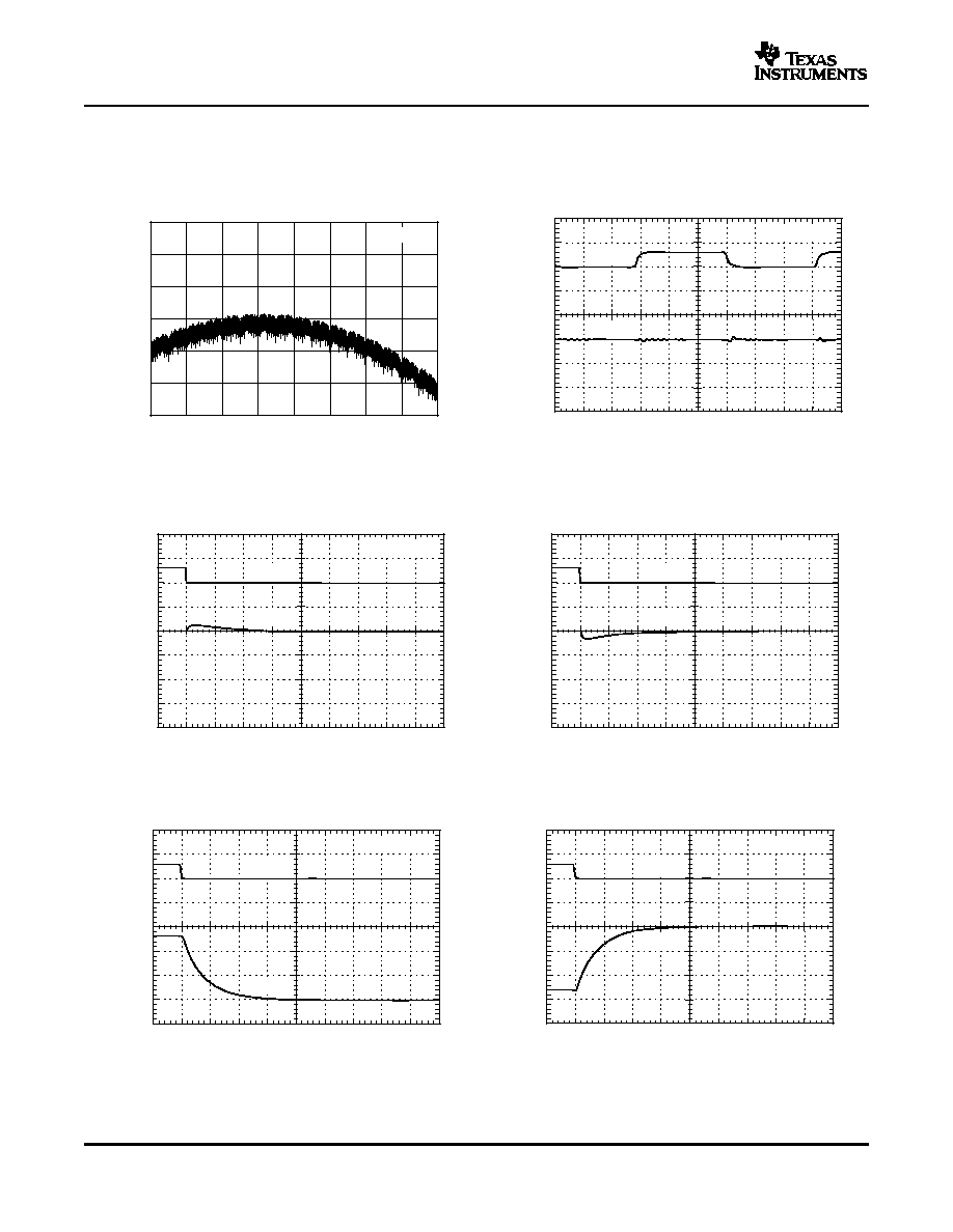
TYPICAL CHARACTERISTICS: V
DD
= 5V (continued)
At T
A
= 25
∞
C, V
REF
= 2.5V unless otherwise noted
MAJOR-CARRY GLITCH
MAJOR-CARRY GLITCH
(FALLING)
(RISING)
Figure 21.
Figure 22.
DAC SETTLING TIME
DAC SETTLING TIME
(FALLING)
(RISING)
Figure 23.
Figure 24.
DIGITAL
FEEDTHROUGH
Figure 25.
11
www.ti.com
TYPICAL CHARACTERISTICS: V
DD
= 3V
8192
0
65536
57344
49152
40960
32768
24576
16384
Digital Input Code
T
A
= +25
_
C
V
REF
= 1.5V
1.00
0.75
0.50
0.25
0
-
0.25
-
0.50
-
0.75
-
1.00
I
N
L
(
L
S
B
)
8192
0
65536
57344
49152
40960
32768
24576
16384
Digital Input Code
T
A
= +25
_
C
V
REF
= 1.5V
1.00
0.75
0.50
0.25
0
-
0.25
-
0.50
-
0.75
-
1.00
D
N
L
(
L
S
B
)
8192
0
65536
57344
49152
40960
32768
24576
16384
Digital Input Code
T
A
=
-
40
_
C
V
REF
= 1.5V
1.00
0.75
0.50
0.25
0
-
0.25
-
0.50
-
0.75
-
1.00
I
N
L
(
L
S
B
)
8192
0
65536
57344
49152
40960
32768
24576
16384
Digital Input Code
T
A
=
-
40
_
C
V
REF
= 1.5V
1.00
0.75
0.50
0.25
0
-
0.25
-
0.50
-
0.75
-
1.00
D
N
L
(
L
S
B
)
8192
0
65536
57344
49152
40960
32768
24576
16384
Digital Input Code
T
A
= +85
_
C
V
REF
= 1.5V
1.00
0.75
0.50
0.25
0
-
0.25
-
0.50
-
0.75
-
1.00
I
N
L
(
L
S
B
)
8192
0
65536
57344
49152
40960
32768
24576
16384
Digital Input Code
T
A
= +85
_
C
V
REF
= 1.5V
1.00
0.75
0.50
0.25
0
-
0.25
-
0.50
-
0.75
-
1.00
D
N
L
(
L
S
B
)
DAC8830
DAC8831
SLAS449A ≠ FEBRUARY 2005 ≠ REVISED MARCH 2005
At T
A
= 25
∞
C, V
REF
= 2.5 V unless otherwise noted
LINEARITY ERROR
DIFFERENTIAL LINEARITY ERROR
vs DIGITAL INPUT CODE
vs DIGITAL INPUT CODE
Figure 26.
Figure 27.
LINEARITY ERROR
DIFFERENTIAL LINEARITY ERROR
vs DIGITAL INPUT CODE
vs DIGITAL INPUT CODE
Figure 28.
Figure 29.
LINEARITY ERROR
DIFFERENTIAL LINEARY ERROR
vs DIGITAL INPUT CODE
vs DIGITAL INPUT CODE
Figure 30.
Figure 31.
12
www.ti.com
8192
0
65536
57344
49152
40960
32768
24576
16384
Digital Input Code
T
A
= +25
_
C
V
REF
= 3V
1.00
0.75
0.50
0.25
0
-
0.25
-
0.50
-
0.75
-
1.00
I
N
L
(
L
S
B
)
8192
0
65536
57344
49152
40960
32768
24576
16384
Digital Input Code
T
A
= +25
_
C
V
REF
= 3V
1.00
0.75
0.50
0.25
0
-
0.25
-
0.50
-
0.75
-
1.00
D
N
L
(
L
S
B
)
-
60
-
40
-
20
0
20
40
60
80
140
120
100
Temperature (
_
C)
V
DD
= 3V
V
REF
= 2.5V
Bipolar Mode
Unipolar Mode
1.00
0.75
0.50
0.25
0
-
0.25
-
0.50
-
0.75
-
1.00
G
a
i
n
E
r
r
o
r
(
L
S
B
)
0.75
0.50
0.25
0
-
0.25
-
0.50
L
i
n
e
a
r
i
t
y
E
r
r
o
r
(
L
S
B
)
Reference Voltage (V)
0.5
1.5
2.5
3.5
3.0
2.0
1.0
DNL
INL
-
60
-
40
-
20
0
20
40
60
80
140
120
100
Temperature (
_
C)
V
DD
= 3V
V
REF
= 2.5V
Bipolar Mode
Unipolar Mode
0.50
0.25
0
-
0.25
-
0.50
-
0.75
Z
e
r
o
-
C
o
d
e
E
r
r
o
r
(
L
S
B
)
8192
0
300
250
200
150
100
50
0
65536
57344
49152
40960
32768
24576
16384
Digital Input Code
R
e
f
e
r
e
n
c
e
C
u
r
r
e
n
t
(
µ
A
)
V
REF
= 1.5V
DAC8830
DAC8831
SLAS449A ≠ FEBRUARY 2005 ≠ REVISED MARCH 2005
TYPICAL CHARACTERISTICS: V
DD
= 3V (continued)
At T
A
= 25
∞
C, V
REF
= 2.5 V unless otherwise noted
LINEARITY ERROR
DIFFERENTIAL LINEARITY ERROR
vs DIGITAL INPUT CODE
vs DIGITAL INPUT CODE
Figure 32.
Figure 33.
LINEARITY ERROR
GAIN ERROR
vs REFERENCE VOLTAGE
vs TEMPERATURE
Figure 34.
Figure 35.
ZERO-CODE ERROR
REFERENCE CURRENT
vs TEMPERATURE
vs CODE (UNIPOLAR MODE)
Figure 36.
Figure 37.
13
www.ti.com
Time (50ns/div)
V
REF
= 2.5V
SDI
V
OUT
5V/div
20mV/div
8192
0
300
250
200
150
100
50
0
65536
57344
49152
40960
32768
24576
16384
Digital Input Code
R
e
f
e
r
e
n
c
e
C
u
r
r
e
n
t
(
µ
A
)
V
REF
= 1.5V
Time (0.5
µ
s/div)
LDAC
V
OUT
V
REF
= 2.5V
5V/div
0.1V/div
Time (0.5
µ
s/div)
V
REF
= 2.5V
LDAC
V
OUT
5V/div
0.1V/div
Time (0.2
µ
s/div)
V
REF
= 2.5V
LDAC
V
OUT
5V/div
1V/div
Time (0.2
µ
s/div)
V
REF
= 2.5V
LDAC
V
OUT
5V/div
1V/div
DAC8830
DAC8831
SLAS449A ≠ FEBRUARY 2005 ≠ REVISED MARCH 2005
TYPICAL CHARACTERISTICS: V
DD
= 3V (continued)
At T
A
= 25
∞
C, V
REF
= 2.5 V unless otherwise noted
REFERENCE CURRENT
DIGITAL
vs CODE (BIPOLAR MODE)
FEEDTHROUGH
Figure 38.
Figure 39.
MAJOR-CARRY GLITCH
MAJOR-CARRY GLITCH
(FALLING)
(RISING)
Figure 40.
Figure 41.
DAC SETTLING TIME
DAC SETTLING TIME
(FALLING)
(RISING)
Figure 42.
Figure 43.
14

www.ti.com
THEORY OF OPERATION
GENERAL DESCRIPTION
DIGITAL-TO-ANALOG SECTIONS
R
R
12-Bit R-2R Ladder
Four MSBs Decoded into
15 Equal Segments
2R
2R
2R
2R
S0
S1
S11
2R
V
OUT
E15
2R
E2
2R
E1
V
REF
OUTPUT RANGE
DAC8830
DAC8831
SLAS449A ≠ FEBRUARY 2005 ≠ REVISED MARCH 2005
The DAC8830 and DAC8831 are single, 16-bit, serial-input, voltage-output DACs. They operate from a single
supply ranging from 2.7V to 5V, and typically consume 5µA. Data is written to these devices in a 16-bit word
format, via an SPI serial interface. To ensure a known power-up state, these parts were designed with a
power-on reset function. The DAC8830 and DAC8831 are reset to zero code. In unipolar mode, the DAC8830
and DAC8831 are reset to 0V, and in bipolar mode, the DAC8831 is reset to ≠V
REF
. Kelvin sense connections for
the reference and analog ground are included on the DAC8831.
The DAC architecture for both devices consists of two matched DAC sections and is segmented. A simplified
circuit diagram is shown in Figure 44. The four MSBs of the 16-bit data word are decoded to drive 15 switches,
E1 to E15. Each of these switches connects one of 15 matched resistors to either AGND or V
REF
. The remaining
12 bits of the data word drive switches S0 to S11 of a 12-bit voltage mode R-2R ladder network.
Figure 44. DAC Architecture
The output of the DAC is
V
OUT
= (V
REF
◊
Code)/65536.
Where Code is the decimal data word loaded to the DAC latch.
15

www.ti.com
POWER-ON RESET
Serial Interface
DAC8830
DAC8831
SLAS449A ≠ FEBRUARY 2005 ≠ REVISED MARCH 2005
THEORY OF OPERATION (continued)
Both devices have a power-on reset function to ensure the output is at a known state upon power-up. In the
DAC8830 and DAC8831, on power-up, the DAC latch and Input Registers contain all 0s until new data is loaded
from the input serial shift register. Therefore, after power-up, the output from pin V
OUT
of the DAC8830 is 0V. The
output from pin V
OUT
of the DAC8831 is 0V in unipolar mode and ≠V
REF
in bipolar mode.
However, the serial register of the DAC8830 and DAC8831 is not cleared on power-up, so its contents are
undefined. When loading data initially to the device, 16 bits or more should be loaded to prevent erroneous data
appearing on the output. If more than 16 bits are loaded, the last 16 are kept; if less than 16 are loaded, bits will
remain from the previous word. If the device must be interfaced with data shorter than 16 bits, the data should be
padded with 0s at the LSBs.
The digital interface is standard 3-wire connection compatible with SPI, QSPI, Microwire, and TI DSP interfaces,
which can operate at speeds up to 50M-bits/sec. The data transfer is framed by CS, the chip select signal. The
DAC works as a bus slave. The bus master generates the synchronize clock, SCLK, and initiates the
transmission. When CS is high, the DAC is not accessed, and the clock SCLK and serial input data SDI are
ignored. The bus master accesses the DAC by driving pin CS low. Immediately following the high-to-low
transition of CS, the serial input data on pin SDI is shifted out from the bus master synchronously on the falling
edge of SCLK, and latched on the rising edge of SCLK into the input shift register, MSB first. The low-to-high
transition of CS transfers the contents of the input shift register to the input register. All data registers are 16-bit.
It takes 16 clocks of SCLK to transfer one data word to the parts. To complete a whole data word, CS must go
high immediately after 16 SCLKs are clocked in. If more than 16 SCLKs are applied during the low state of CS,
the last 16 bits are transferred to the input register on the rising edge of CS. However, if CS is not kept low
during the entire 16 SCLK cycles, data is corrupted. In this case, reload the DAC latch with a new 16-bit word.
In the DAC8830, the contents of the input register are transferred into the DAC latch immediately when the input
register is loaded, and the DAC output is updated at the same time.
The DAC8831 has an LDAC pin allowing the DAC latch to be updated asynchronously by bringing LDAC low
after CS goes high. In this case, LDAC must be maintained high while CS is low. If LDAC is tied permanently
low, the DAC latch is updated immediately after the input register is loaded (caused by the low-to-high transition
of CS).
16
www.ti.com
APPLICATION INFORMATION
Unipolar Output Operation
DAC
DAC8830
SDI
SCLK
CS
DGND
V
OUT
0.1
µ
F
V
O
= 0 to +V
REF
AGND
S
e
r
i
a
l
I
n
t
e
r
f
a
c
e
Input
Register
DAC Latch
V
DD
V
REF
+5V
+2.5V
OPA277
OPA704
OPA727
+
0.1
µ
F
10
µ
F
DAC8830
DAC8831
SLAS449A ≠ FEBRUARY 2005 ≠ REVISED MARCH 2005
These DACs are capable of driving unbuffered loads of 60k
. Unbuffered operation results in low supply current
(typically 5µA) and a low offset error. The DAC8830 provides a unipolar output swing ranging from 0V to V
REF
.
The DAC8831 can be configured to output both unipolar and bipolar voltages. Figure 45 and Figure 46 show a
typical unipolar output voltage circuit for each device, respectively. The code table for this mode of operation is
shown in Table 1.
Table 1. Unipolar Code
DAC Latch Contents
MSB
LSB
Analog Output
1111 1111 1111 1111
V
REF
◊
(65,535/65,536)
1000 0000 0000 0000
V
REF
◊
(32,768/65,536) = 1/2 V
REF
0000 0000 0000 0001
V
REF
◊
(1/65,536)
0000 0000 0000 0000
0V
Figure 45. Unipolar Output Mode of DAC8830
17
www.ti.com
0.1
µ
F
V
DD
+5V
RFB
INV
AGNDF
AGNDS
DAC
DAC Latch
Input
Register
DAC8831
+V
-
V
SDI
SCLK
LDAC
V
OUT
R
FB
R
INV
V
REF
-
S
V
REF
-
F
S
e
r
i
a
l
I
n
t
e
r
f
a
c
e
a
n
d
C
o
n
t
r
o
l
L
o
g
i
c
CS
+2.5V
+
0.1
µ
F
10
µ
F
DGND
V
O
= 0 to +V
REF
OPA277
OPA704
OPA727
V
OUT
*
UNI
D
2
16
V
REF
)
V
GE
)
V
ZSE
)
INL
DAC8830
DAC8831
SLAS449A ≠ FEBRUARY 2005 ≠ REVISED MARCH 2005
Figure 46. Unipolar Output Mode of DAC8831
Assuming a perfect reference, the worst-case output voltage may be calculated from the following equation:
Unipolar Mode Worst-Case Output
Where:
V
OUT_UNI
= Unipolar mode worst-case output
D = Code loaded to DAC
V
REF
= Reference voltage applied to part
V
GE
= Gain error in volts
V
ZSE
= Zero scale error in volts
INL = Integral nonlinearity in volts
18
www.ti.com
Bipolar Output Operation
0.1
µ
F
V
DD
+5V
RFB
INV
AGNDF
AGNDS
DAC
DAC Latch
Input
Register
DAC8831
+V
-
V
SDI
SCLK
LDAC
V
OUT
R
FB
R
INV
V
REF
-
S
V
REF
-
F
S
e
r
i
a
l
I
n
t
e
r
f
a
c
e
a
n
d
C
o
n
t
r
o
l
L
o
g
i
c
CS
+2.5V
+
0.1
µ
F
10
µ
F
DGND
V
O
=
-
V
REF
to +V
REF
OPA277
OPA704
OPA727
V
OUT
)
BIP
*
V
OUT
)
UNI
V
OS
(2
RD)
)
V
REF
(1
RD)
1
2
RD
A
DAC8830
DAC8831
SLAS449A ≠ FEBRUARY 2005 ≠ REVISED MARCH 2005
With the aid of an external operational amplifier, the DAC8831 may be configured to provide a bipolar voltage
output. A typical circuit of such an operation is shown in Figure 47. The matched bipolar offset resistors R
FB
and
R
INV
are connected to an external operational amplifier to achieve this bipolar output swing; typically, R
FB
= R
INV
= 28k
.
Table 2 shows the transfer function for this output operating mode. The DAC8831 also provides a set of Kelvin
connections to the analog ground and external reference inputs.
Table 2. Bipolar Code
DAC Latch Contents
MSB
LSB
Analog Output
1111 1111 1111 1111
+V
REF
◊
(32,767/32,768)
1000 0000 0000 0000
+V
REF
◊
(1/32,768)
0111 1111 1111 1111
0V
0000 0000 0000 0001
≠V
REF
◊
(1/32,768)
0000 0000 0000 0000
≠V
REF
◊
(32,767/32,768) = ≠V
REF
Figure 47. Bipolar Output Mode of DAC8831
Assuming a perfect reference, the worst-case output voltage may be calculated from the following equation:
Bipolar Mode Worst-Case Output
Where:
V
OS
= External operational amplifier input offset voltage
RD = R
FB
and R
IN
resistor matching error
A = Operational amplifier open-loop gain
19

www.ti.com
Output Amplifier Selection
Reference and Ground
Power Supply and Reference Bypassing
DAC8830
DAC8831
SLAS449A ≠ FEBRUARY 2005 ≠ REVISED MARCH 2005
For bipolar mode, a precision amplifier should be used, supplied from a dual power supply. This provides the
±
V
REF
output.
In a single-supply application, selection of a suitable operational amplifier may be more difficult because the
output swing of the amplifier does not usually include the negative rail; in this case, AGND. This output swing can
result in some degradation of the specified performance unless the application does not use codes near 0.
The selected operational amplifier needs to have low-offset voltage (the DAC LSB is 38µV with a 2.5V
reference), eliminating the need for output offset trims. Input bias current should also be low because the bias
current multiplied by the DAC output impedance (approximately 6.25k
) adds to the zero-code error.
Rail-to-rail input and output performance is required. For fast settling, the slew rate of the operational amplifier
should not impede the settling time of the DAC. Output impedance of the DAC is constant and
code-independent, but in order to minimize gain errors the input impedance of the output amplifier should be as
high as possible. The amplifier should also have a 3dB bandwidth of 1MHz or greater. The amplifier adds
another time constant to the system, thus increasing the settling time of the output. A higher 3dB amplifier
bandwidth results in a shorter effective settling time of the combined DAC and amplifier.
Since the input impedance is code-dependent, the reference pin should be driven from a low impedance source.
The DAC8830 and DAC8831 operate with a voltage reference ranging from 1.25V to V
DD
. References below
1.25V result in reduced accuracy.
The DAC full-scale output voltage is determined by the reference. Table 1 and Table 2 outline the analog output
voltage for particular digital codes.
For optimum performance, Kelvin sense connections are provided on the DAC8831. If the application does not
require separate force and sense lines, they should be tied together close to the package to minimize voltage
drops between the package leads and the internal die.
For accurate high-resolution performance, it is recommended that the reference and supply pins be bypassed
with a 10µF tantalum capacitor in parallel with a 0.1µF ceramic capacitor.
20

www.ti.com
CROSS REFERENCE
DAC8830
DAC8831
SLAS449A ≠ FEBRUARY 2005 ≠ REVISED MARCH 2005
The DAC8830 and DAC8831 have an industry-standard pinout configuration (see Table 3).
Table 3. Cross Reference
INL
DNL
POWER-ON
TEMPERATURE
PACKAGE
PACKAGE
CROSS
MODEL
(LSB)
(LSB)
RESET TO
RANGE
DESCRIPTION
OPTION
REFERENCE
AD5541CR,
DAC8830ICD
±
1
±
1
Zero-Code
≠40
∞
C to +85
∞
C
8-Lead Small Outline IC
SO-8
MAX541AESA
AD5541BR,
DAC8830IBD
±
2
±
1
Zero-Code
≠40
∞
C to +85
∞
C
8-Lead Small Outline IC
SO-8
MAX541BESA
AD5541AR,
DAC8830ID
±
4
±
1
Zero-Code
≠40
∞
C to +85
∞
C
8-Lead Small Outline IC
SO-8
MAX541CESA
N/A
±
1
±
1
Zero-Code
≠40
∞
C to +85
∞
C
8-Lead Plastic DIP
PDIP-8
MAX541AEPA
N/A
±
2
±
1
Zero-Code
≠40
∞
C to +85
∞
C
8-Lead Plastic DIP
PDIP-8
MAX541BEPA
N/A
±
4
±
1
Zero-Code
≠40
∞
C to +85
∞
C
8-Lead Plastic DIP
PDIP-8
MAX541CEPA
N/A
±
1
±
1
Zero-Code
0
∞
C to +70
∞
C
8-Lead Small Outline IC
SO-8
AD5541LR
N/A
±
2
±
1.5
Zero-Code
0
∞
C to +70
∞
C
8-Lead Small Outline IC
SO-8
AD5541JR
N/A
±
1
±
1
Zero-Code
0
∞
C to +70
∞
C
8-Lead Plastic DIP
PDIP-8
MAX541AEPA
N/A
±
2
±
1
Zero-Code
0
∞
C to +70
∞
C
8-Lead Plastic DIP
PDIP-8
MAX541BEPA
N/A
±
4
±
1
Zero-Code
0
∞
C to +70
∞
C
8-Lead Plastic DIP
PDIP-8
MAX541CEPA
AD5542CR,
DAC8831ICD
±
1
±
1
Zero-Code
≠40
∞
C to +85
∞
C
14-Lead Small Outline IC
SO-14
MAX542AESD
AD5542BR,
DAC8831IBD
±
2
±
1
Zero-Code
-40
∞
C to +85
∞
C
14-Lead Small Outline IC
SO-14
MAX542BESD
AD5542AR,
DAC8831ID
±
4
±
1
Zero-Code
≠40
∞
C to +85
∞
C
14-Lead Small Outline IC
SO-14
MAX542CESD
N/A
±
1
±
1
Zero-Code
≠40
∞
C to +85
∞
C
14-Lead Plastic DIP
PDIP-14
MAX542ACPD
N/A
±
2
±
1
Zero-Code
≠40
∞
C to +85
∞
C
14-Lead Plastic DIP
PDIP-14
MAX542BCPD
N/A
±
4
±
1
Zero-Code
≠40
∞
C to +85
∞
C
14-Lead Plastic DIP
PDIP-14
MAX542CCPD
N/A
±
1
±
1
Zero-Code
0
∞
C to +70
∞
C
14-Lead Small Outline IC
SO-14
AD5542LR
N/A
±
2
±
1.5
Zero-Code
0
∞
C to +70
∞
C
14-Lead Small Outline IC
SO-14
AD5542JR
N/A
±
1
±
1
Zero-Code
0
∞
C to +70
∞
C
14-Lead Small Outline IC
SO-14
MAX542AEPD
N/A
±
2
±
1
Zero-Code
0
∞
C to +70
∞
C
14-Lead Small Outline IC
SO-14
MAX542BEPD
N/A
±
4
±
1
Zero-Code
0
∞
C to +70
∞
C
14-Lead Small Outline IC
SO-14
MAX542CEPD
21
PACKAGING INFORMATION
Orderable Device
Status
(1)
Package
Type
Package
Drawing
Pins Package
Qty
Eco Plan
(2)
Lead/Ball Finish
MSL Peak Temp
(3)
DAC8830IBDR
ACTIVE
SOIC
D
8
2500
TBD
CU NIPDAU
Level-3-240C-168 HR
DAC8830IBDT
ACTIVE
SOIC
D
8
250
TBD
CU NIPDAU
Level-3-240C-168 HR
DAC8830ICDR
ACTIVE
SOIC
D
8
2500
TBD
CU NIPDAU
Level-3-240C-168 HR
DAC8830ICDT
ACTIVE
SOIC
D
8
250
TBD
CU NIPDAU
Level-3-240C-168 HR
DAC8830IDR
ACTIVE
SOIC
D
8
2500
TBD
CU NIPDAU
Level-3-240C-168 HR
DAC8830IDT
ACTIVE
SOIC
D
8
250
TBD
CU NIPDAU
Level-3-240C-168 HR
DAC8831IBD
ACTIVE
SOIC
D
14
58
TBD
CU NIPDAU
Level-3-240C-168 HR
DAC8831IBDR
ACTIVE
SOIC
D
14
2500
TBD
CU NIPDAU
Level-3-240C-168 HR
DAC8831ICD
ACTIVE
SOIC
D
14
58
TBD
CU NIPDAU
Level-3-240C-168 HR
DAC8831ICDR
ACTIVE
SOIC
D
14
2500
TBD
CU NIPDAU
Level-3-240C-168 HR
DAC8831ID
ACTIVE
SOIC
D
14
58
TBD
CU NIPDAU
Level-3-240C-168 HR
DAC8831IDR
ACTIVE
SOIC
D
14
2500
TBD
CU NIPDAU
Level-3-240C-168 HR
(1)
The marketing status values are defined as follows:
ACTIVE: Product device recommended for new designs.
LIFEBUY: TI has announced that the device will be discontinued, and a lifetime-buy period is in effect.
NRND: Not recommended for new designs. Device is in production to support existing customers, but TI does not recommend using this part in
a new design.
PREVIEW: Device has been announced but is not in production. Samples may or may not be available.
OBSOLETE: TI has discontinued the production of the device.
(2)
Eco
Plan
-
The
planned
eco-friendly
classification:
Pb-Free
(RoHS)
or
Green
(RoHS
&
no
Sb/Br)
-
please
check
http://www.ti.com/productcontent
for the latest availability information and additional product content details.
TBD: The Pb-Free/Green conversion plan has not been defined.
Pb-Free (RoHS): TI's terms "Lead-Free" or "Pb-Free" mean semiconductor products that are compatible with the current RoHS requirements
for all 6 substances, including the requirement that lead not exceed 0.1% by weight in homogeneous materials. Where designed to be soldered
at high temperatures, TI Pb-Free products are suitable for use in specified lead-free processes.
Green (RoHS & no Sb/Br): TI defines "Green" to mean Pb-Free (RoHS compatible), and free of Bromine (Br) and Antimony (Sb) based flame
retardants (Br or Sb do not exceed 0.1% by weight in homogeneous material)
(3)
MSL, Peak Temp. -- The Moisture Sensitivity Level rating according to the JEDEC industry standard classifications, and peak solder
temperature.
Important Information and Disclaimer:The information provided on this page represents TI's knowledge and belief as of the date that it is
provided. TI bases its knowledge and belief on information provided by third parties, and makes no representation or warranty as to the
accuracy of such information. Efforts are underway to better integrate information from third parties. TI has taken and continues to take
reasonable steps to provide representative and accurate information but may not have conducted destructive testing or chemical analysis on
incoming materials and chemicals. TI and TI suppliers consider certain information to be proprietary, and thus CAS numbers and other limited
information may not be available for release.
In no event shall TI's liability arising out of such information exceed the total purchase price of the TI part(s) at issue in this document sold by TI
to Customer on an annual basis.
PACKAGE OPTION ADDENDUM
www.ti.com
3-Oct-2005
Addendum-Page 1


IMPORTANT NOTICE
Texas Instruments Incorporated and its subsidiaries (TI) reserve the right to make corrections, modifications,
enhancements, improvements, and other changes to its products and services at any time and to discontinue
any product or service without notice. Customers should obtain the latest relevant information before placing
orders and should verify that such information is current and complete. All products are sold subject to TI's terms
and conditions of sale supplied at the time of order acknowledgment.
TI warrants performance of its hardware products to the specifications applicable at the time of sale in
accordance with TI's standard warranty. Testing and other quality control techniques are used to the extent TI
deems necessary to support this warranty. Except where mandated by government requirements, testing of all
parameters of each product is not necessarily performed.
TI assumes no liability for applications assistance or customer product design. Customers are responsible for
their products and applications using TI components. To minimize the risks associated with customer products
and applications, customers should provide adequate design and operating safeguards.
TI does not warrant or represent that any license, either express or implied, is granted under any TI patent right,
copyright, mask work right, or other TI intellectual property right relating to any combination, machine, or process
in which TI products or services are used. Information published by TI regarding third-party products or services
does not constitute a license from TI to use such products or services or a warranty or endorsement thereof.
Use of such information may require a license from a third party under the patents or other intellectual property
of the third party, or a license from TI under the patents or other intellectual property of TI.
Reproduction of information in TI data books or data sheets is permissible only if reproduction is without
alteration and is accompanied by all associated warranties, conditions, limitations, and notices. Reproduction
of this information with alteration is an unfair and deceptive business practice. TI is not responsible or liable for
such altered documentation.
Resale of TI products or services with statements different from or beyond the parameters stated by TI for that
product or service voids all express and any implied warranties for the associated TI product or service and
is an unfair and deceptive business practice. TI is not responsible or liable for any such statements.
Following are URLs where you can obtain information on other Texas Instruments products and application
solutions:
Products
Applications
Amplifiers
amplifier.ti.com
Audio
www.ti.com/audio
Data Converters
dataconverter.ti.com
Automotive
www.ti.com/automotive
DSP
dsp.ti.com
Broadband
www.ti.com/broadband
Interface
interface.ti.com
Digital Control
www.ti.com/digitalcontrol
Logic
logic.ti.com
Military
www.ti.com/military
Power Mgmt
power.ti.com
Optical Networking
www.ti.com/opticalnetwork
Microcontrollers
microcontroller.ti.com
Security
www.ti.com/security
Telephony
www.ti.com/telephony
Video & Imaging
www.ti.com/video
Wireless
www.ti.com/wireless
Mailing Address:
Texas Instruments
Post Office Box 655303 Dallas, Texas 75265
Copyright
2005, Texas Instruments Incorporated