 | –≠–ª–µ–∫—Ç—Ä–æ–Ω–Ω—ã–π –∫–æ–º–ø–æ–Ω–µ–Ω—Ç: DAC904U | –°–∫–∞—á–∞—Ç—å:  PDF PDF  ZIP ZIP |

Æ
DAC904
1
DAC904
DAC904
Æ
DAC904
©
1999 Burr-Brown Corporation
PDS-1448B
Printed in U.S.A. May, 2000
International Airport Industrial Park ∑ Mailing Address: PO Box 11400, Tucson, AZ 85734 ∑ Street Address: 6730 S. Tucson Blvd., Tucson, AZ 85706 ∑ Tel: (520) 746-1111
Twx: 910-952-1111 ∑ Internet: http://www.burr-brown.com/ ∑ Cable: BBRCORP ∑ Telex: 066-6491 ∑ FAX: (520) 889-1510 ∑ Immediate Product Info: (800) 548-6132
For most current data sheet and other product
information, visit www.burr-brown.com
14-Bit, 165MSPS
DIGITAL-TO-ANALOG CONVERTER
FEATURES
q
SINGLE +5V OR +3V OPERATION
q
HIGH SFDR: 20MHz Output at 100MSPS: 64dBc
q
LOW GLITCH: 3pV-s
q
LOW POWER: 170mW at +5V
q
INTERNAL REFERENCE:
Optional Ext. Reference
Adjustable Full-Scale Range
Multiplying Option
APPLICATIONS
q
COMMUNICATION TRANSMIT CHANNELS
WLL, Cellular Base Station
Digital Microwave Links
Cable Modems
q
WAVEFORM GENERATION
Direct Digital Synthesis (DDS)
Arbitrary Waveform Generation (ARB)
q
MEDICAL/ULTRASOUND
q
HIGH-SPEED INSTRUMENTATION AND
CONTROL
q
VIDEO, DIGITAL TV
DESCRIPTION
The DAC904 is a high-speed, digital-to-analog converter (DAC)
offering a 14-bit resolution option within the SpeedPlus family
of high-performance converters. Featuring pin compatibility
among family members, the DAC908, DAC900, and DAC902
provide a component selection option to an 8-, 10-, and 12-bit
resolution, respectively. All models within this family of D/A
converters support update rates in excess of 165MSPS with
excellent dynamic performance, and are especially suited to
fulfill the demands of a variety of applications.
The advanced segmentation architecture of the DAC904 is
optimized to provide a high Spurious-Free Dynamic Range
(SFDR) for single-tone, as well as for multi-tone signals--
essential when used for the transmit signal path of communica-
tion systems.
The DAC904 has a high impedance (200k
) current output with
a nominal range of 20mA and an output compliance of up to
1.25V. The differential outputs allow for both a differential, or
single-ended analog signal interface. The close matching of the
current outputs ensures superior dynamic performance in the
differential configuration, which can be implemented with a
transformer.
Utilizing a small geometry CMOS process, the monolithic
DAC904 can be operated on a wide, single-supply range of
+2.7V to +5.5V. Its low power consumption allows for use in
portable and battery operated systems. Further optimization can
be realized by lowering the output current with the adjustable
full-scale option.
For noncontinuous operation of the DAC904, a power-down
mode results in only 45mW of standby power.
The DAC904 comes with an integrated 1.24V bandgap refer-
ence and edge-triggered input latches, offering a complete
converter solution. Both +3V and +5V CMOS logic families
can be interfaced to the DAC904.
The reference structure of the DAC904 allows for additional
flexibility by utilizing the on-chip reference, or applying an
external reference. The full-scale output current can be adjusted
over a span of 2mA to 20mA, with one external resistor, while
maintaining the specified dynamic performance.
The DAC904 is available in SO-28 and TSSOP-28 packages.
TM
Current
Sources
LSB
Switches
Segmented
Switches
+1.24V Ref.
Latches
14-Bit Data Input
D13...D0
DAC904
FSA
BW
+V
D
+V
A
AGND
CLK
DGND
REF
IN
INT/EXT
I
OUT
I
OUT
BYP
PD

Æ
DAC904
2
SPECIFICATIONS
At T
A
= full specified temperature range, +V
A
= +5V, +V
D
= +5V, differential transformer coupled output, 50
doubly terminated, unless otherwise specified.
The information provided herein is believed to be reliable; however, BURR-BROWN assumes no responsibility for inaccuracies or omissions. BURR-BROWN assumes
no responsibility for the use of this information, and all use of such information shall be entirely at the user's own risk. Prices and specifications are subject to change
without notice. No patent rights or licenses to any of the circuits described herein are implied or granted to any third party. BURR-BROWN does not authorize or warrant
any BURR-BROWN product for use in life support devices and/or systems.
DAC904U/E
PARAMETER
CONDITIONS
MIN
TYP
MAX
UNITS
Resolution
14
Bits
Output Update Rate (f
CLOCK
)
4.5V to 5.5V
165
200
MSPS
Output Update Rate
2.7V to 3.3V
125
165
MSPS
Full Specified Temperature Range, Operating
Ambient, T
A
≠40
+85
∞
C
STATIC ACCURACY
(1)
T
A
= +25
∞
C
Differential Nonlinearity (DNL)
f
CLOCK
= 25MSPS, f
OUT
= 1.0MHz
±
2.5
LSB
Integral Nonlinearity (INL)
±
3.0
LSB
DYNAMIC PERFORMANCE
T
A
= +25
∞
C
Spurious Free Dynamic Range (SFDR)
To Nyquist
f
OUT
= 1.0MHz, f
CLOCK
= 25MSPS
72
79
dBc
f
OUT
= 2.1MHz, f
CLOCK
= 50MSPS
76
dBc
f
OUT
= 5.04MHz, f
CLOCK
= 50MSPS
68
dBc
f
OUT
= 5.04MHz, f
CLOCK
= 100MSPS
68
dBc
f
OUT
= 20.2MHz, f
CLOCK
= 100MSPS
64
dBc
f
OUT
= 25.3MHz, f
CLOCK
= 125MSPS
60
dBc
f
OUT
= 41.5MHz, f
CLOCK
= 125MSPS
55
dBc
f
OUT
= 27.4MHz, f
CLOCK
= 165MSPS
60
dBc
f
OUT
= 54.8MHz, f
CLOCK
= 165MSPS
55
dBc
Spurious Free Dynamic Range within a Window
f
OUT
= 5.04MHz, f
CLOCK
= 50MSPS
2MHz Span
82
dBc
f
OUT
= 5.04MHz, f
CLOCK
= 100MSPS
4MHz Span
82
dBc
Total Harmonic Distortion (THD)
f
OUT
= 2.1MHz, f
CLOCK
= 50MSPS
≠75
dBc
f
OUT
= 2.1MHz, f
CLOCK
= 125MSPS
≠74
dBc
Two Tone
f
OUT1
= 13.5MHz, f
OUT2
= 14.5MHz, f
CLOCK
= 100MSPS
63
dBc
Output Settling Time
(2)
to 0.1%
30
ns
Output Rise Time
(2)
10% to 90%
2
ns
Output Fall Time
(2)
10% to 90%
2
ns
Glitch Impulse
3
pV-s
DC-ACCURACY
Full-Scale Output Range
(3)
(FSR)
All Bits High, I
OUT
2.0
20.0
mA
Output Compliance Range
≠1.0
+1.25
V
Gain Error
With Internal Reference
≠10
±
1
+10
%FSR
Gain Error
With External Reference
≠10
±
2
+10
%FSR
Gain Drift
With Internal Reference
±
120
ppmFSR/
∞
C
Offset Error
With Internal Reference
≠0.025
+0.025
%FSR
Offset Drift
With Internal Reference
±
0.1
ppmFSR/
∞
C
Power Supply Rejection, +V
A
≠0.2
+0.2
%FSR/V
Power Supply Rejection, +V
D
≠0.025
+0.025
%FSR/V
Output Noise
I
OUT
= 20mA, R
LOAD
= 50
50
pA/
Hz
Output Resistance
200
k
Output Capacitance
I
OUT
, I
OUT
to Ground
12
pF
REFERENCE
Reference Voltage
+1.24
V
Reference Tolerance
±
10
%
Reference Voltage Drift
±
50
ppmFSR/
∞
C
Reference Output Current
10
µ
A
Reference Input Resistance
1
M
Reference Input Compliance Range
0.1
1.25
V
Reference Small Signal Bandwidth
(4)
1.3
MHz
DIGITAL INPUTS
Logic Coding
Straight Binary
Latch Command
Rising Edge of Clock
Logic High Voltage, V
IH
+V
D
= +5V
3.5
5
V
Logic Low Voltage, V
IL
+V
D
= +5V
0
1.2
V
Logic High Voltage, V
IH
+V
D
= +3V
2
3
V
Logic Low Voltage, V
IL
+V
D
= +3V
0
0.8
V
Logic High Current
,
I
IH
(5)
+V
D
= +5V
±
20
µ
A
Logic Low Current, I
IL
+V
D
= +5V
±
20
µ
A
Input Capacitance
5
pF

Æ
DAC904
3
SPECIFICATIONS
(Cont.)
At T
A
= +25
∞
C, +V
A
= +5V, +V
D
= +5V, differential transformer coupled output, 50
doubly terminated, unless otherwise specified.
DAC904U/E
PARAMETER
CONDITIONS
MIN
TYP
MAX
UNITS
ELECTROSTATIC
DISCHARGE SENSITIVITY
This integrated circuit can be damaged by ESD. Burr-Brown
recommends that all integrated circuits be handled with
appropriate precautions. Failure to observe proper handling
and installation procedures can cause damage.
ESD damage can range from subtle performance degradation
to complete device failure. Precision integrated circuits may
be more susceptible to damage because very small parametric
changes could cause the device not to meet its published
specifications.
PACKAGE
SPECIFIED
DRAWING
TEMPERATURE
PACKAGE
ORDERING
TRANSPORT
PRODUCT
PACKAGE
NUMBER
RANGE
MARKING
NUMBER
(1)
MEDIA
DAC904U
SO-28
217
≠40
∞
C to +85
∞
C
DAC904U
DAC904U
Rails
"
"
"
"
"
DAC904U/1K
Tape and Reel
DAC904E
TSSOP-28
360
≠40
∞
C to +85
∞
C
DAC904E
DAC904E
Rails
"
"
"
"
"
DAC904E/2K5
Tape and Reel
NOTE: (1) Models with a slash (/) are available only in Tape and Reel in the quantities indicated (e.g., /2K5 indicates 2500 devices per reel). Ordering 2500 pieces
of "DAC904E/2K5" will get a single 2500-piece Tape and Reel.
PACKAGE/ORDERING INFORMATION
DEMO BOARD
PRODUCT
ORDERING NUMBER
COMMENT
DAC904U
DEM-DAC90xU
Populated evaluation board without D/A converter. Order sample of desired DAC90x model separately.
DAC904E
DEM-DAC904E
Populated evaluation board including the DAC904E.
DEMO BOARD ORDERING INFORMATION
ABSOLUTE MAXIMUM RATINGS
+VA
to AGND ........................................................................ ≠0.3V to +6V
+VD
to DGND ........................................................................ ≠0.3V to +6V
AGND
to DGND ................................................................. ≠0.3V to +0.3V
+VA to +VD .............................................................................. ≠6V to +6V
CLK, PD to DGND ...................................................... ≠0.3V to VD + 0.3V
D0-D13 to DGND ........................................................ ≠0.3V to VD + 0.3V
I
OUT
, I
OUT
to AGND ............................................................ ≠1V to VA + 0.3V
BW, BYP to AGND ....................................................... ≠0.3V to VA + 0.3V
REFIN, FSA to AGND .................................................. ≠0.3V to VA + 0.3V
INT/EXT to AGND ........................................................ ≠0.3V to VA + 0.3V
Junction Temperature .................................................................... +150
∞
C
Case Temperature ......................................................................... +100
∞
C
Storage Temperature ..................................................................... +125
∞
C
POWER SUPPLY
Supply Voltages
+V
A
+2.7
+5
+5.5
V
+V
D
+2.7
+5
+5.5
V
Supply Current
(6)
I
VA
24
30
mA
I
VA
, Power-Down Mode
1.1
2
mA
I
VD
8
15
mA
Power Dissipation
+5V, I
OUT
= 20mA
170
230
mW
+3V, I
OUT
= 2mA
50
mW
Power Dissipation, Power-Down Mode
45
mW
Thermal Resistance,
JA
SO-28
75
∞
C/W
TSSOP-28
50
∞
C/W
NOTES: (1) At output I
OUT
, while driving a virtual ground. (2) Measured single-ended into 50
Load. (3) Nominal full-scale output current is 32x I
REF
; see Application
Section for details. (4) Reference bandwidth depends on size of external capacitor at the BW pin and signal level. (5) Typically 45
µ
A for the PD pin, which has an
internal pull-down resistor. (6) Measured at f
CLOCK
= 50MSPS and f
OUT
= 1.0MHz.

Æ
DAC904
4
Current
Sources
LSB
Switches
Segmented
MSB
Switches
+1.24V Ref.
Latches
14-Bit Data Input
D13.......D0
DAC904
FSA
BW
+V
D
+V
A
R
SET
AGND
CLK
DGND
REF
IN
0.1
µ
F
INT/EXT
I
OUT
I
OUT
BYP
PD
20pF
50
50
20pF
1:1
0.1
µ
F
0.1
µ
F
+5V
+5V
Bit 1
Bit 2
Bit 3
Bit 4
Bit 5
Bit 6
Bit 7
Bit 8
Bit 9
Bit 10
Bit 11
Bit 12
Bit 13
Bit 14
CLK
+V
D
DGND
NC
+V
A
BYP
I
OUT
I
OUT
AGND
BW
FSA
REF
IN
INT/EXT
PD
1
2
3
4
5
6
7
8
9
10
11
12
13
14
28
27
26
25
24
23
22
21
20
19
18
17
16
15
DAC904
PIN
DESIGNATOR
DESCRIPTION
1
Bit 1
Data Bit 1 (D13), MSB
2
Bit 2
Data Bit 2 (D12)
3
Bit 3
Data Bit 3 (D11)
4
Bit 4
Data Bit 4 (D10)
5
Bit 5
Data Bit 5 (D9)
6
Bit 6
Data Bit 6 (D8)
7
Bit 7
Data Bit 7 (D7)
8
Bit 8
Data Bit 8 (D6)
9
Bit 9
Data Bit 9 (D5)
10
Bit 10
Data Bit 10 (D4)
11
Bit 11
Data Bit 11 (D3)
12
Bit 12
Data Bit 12 (D2)
13
Bit 13
Data Bit 13 (D1)
14
Bit 14
Data Bit 14 (D0), LSB
15
PD
Power Down, Control Input; Active
High. Contains internal pull-down circuit;
may be left unconnected if not used.
16
INT/EXT
Reference Select Pin; Internal ( = 0) or
External ( = 1) Reference Operation.
17
REF
IN
Reference Input/Ouput. See Applications
section for further details.
18
FSA
Full-Scale Output Adjust
19
BW
Bandwidth/Noise Reduction Pin:
Bypass with 0.1
µ
F to +V
A
for Optimum
Performance.
20
AGND
Analog Ground
21
I
OUT
Complementary DAC Current Output
22
I
OUT
DAC Current Output
23
BYP
Bypass Node: Use 0.1
µ
F to AGND
24
+V
A
Analog Supply Voltage, 2.7V to 5.5V
25
NC
No Connection
26
DGND
Digital Ground
27
+V
D
Digital Supply Voltage, 2.7V to 5.5V
28
CLK
Clock Input
PIN DESCRIPTIONS
PIN CONFIGURATION
Top View
SO/TSSOP
TYPICAL CONNECTION CIRCUIT

Æ
DAC904
5
TIMING DIAGRAM
t
2
t
PD
t
SET
t
H
t
S
t
1
CLK
D13- D0
I
OUT
SYMBOL
DESCRIPTION
MIN
TYP
MAX
UNITS
t
1
Clock Pulse High Time
6.25
ns
t
2
Clock Pulse Low Time
6.25
ns
t
S
Data Setup Time
2
ns
t
H
Data Hold Time
2
ns
t
PD
Propagation Delay Time
(t
1
+t
2
)+1
ns
t
SET
Output Settling Time to 0.1%
25
ns

Æ
DAC904
6
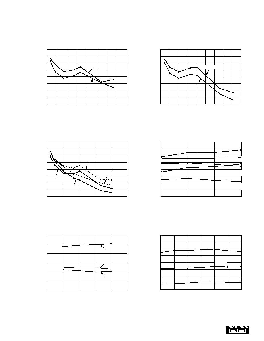
TYPICAL PERFORMANCE CURVES, V
D
= V
A
= +5V
At T
A
= +25
∞
C, Differential I
OUT
= 20mA, 50
double-terminated load, SFDR up to Nyquist, unless otherwise specified.
SFDR vs f
OUT
AT 25MSPS
Frequency (MHz)
SFDR (dBc)
90
85
80
75
70
65
60
2.0
4.0
6.0
8.0
10.0
12.0
0
0dBFS
≠6dBFS
SFDR vs f
OUT
AT 50MSPS
Frequency (MHz)
SFDR (dBc)
85
80
75
70
65
60
55
5.0
10.0
15.0
20.0
25.0
0
≠6dBFS
0dBFS
SFDR vs f
OUT
AT 100MSPS
Frequency (MHz)
SFDR (dBc)
85
80
75
70
65
60
55
50
45
10.0
20.0
30.0
40.0
50.0
0
0dBFS
≠6dBFS
SFDR vs f
OUT
AT 125MSPS
Frequency (MHz)
SFDR (dBc)
85
80
75
70
65
60
55
50
45
10.0
20.0
30.0
50.0
40.0
60.0
0
0dBFS
≠6dBFS
DAC Code
TYPICAL DNL
Error (LSBs)
10
8
6
4
2
0
≠2
≠4
≠6
≠8
≠10
0
2k
4k
6k
8k
10k
12k
14k
16k
16384
TYPICAL INL
Error (LSBs)
10
8
6
4
2
0
≠2
≠4
≠6
≠8
≠10
DAC Code
0
2k
4k
6k
8k
10k
12k
14k
16k
16384
Æ
DAC904
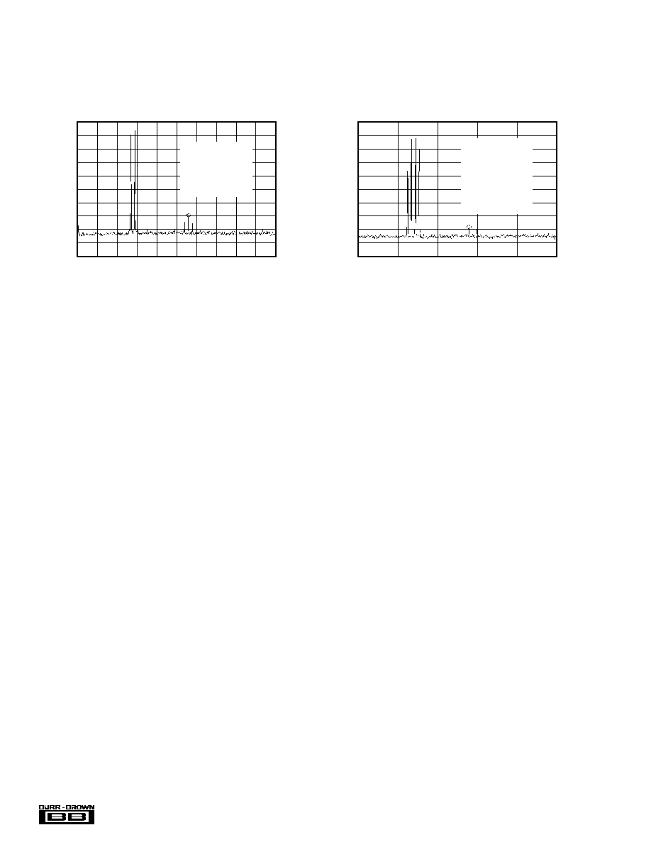
7
TYPICAL PERFORMANCE CURVES, V
D
= V
A
= +5V (Cont.)
At T
A
= +25
∞
C, Differential I
OUT
= 20mA, 50
double-terminated load, SFDR up to Nyquist, unless otherwise specified.
SFDR vs f
OUT
AT 165MSPS
Frequency (MHz)
SFDR (dBc)
80
75
70
65
60
55
50
45
40
20.0
10.0
30.0
40.0
50.0
70.0
60.0
80.0
0
≠6dBFS
0dBFS
SFDR vs I
OUTFS
and f
OUT
AT 100MSPS, 0dBFS
I
OUTFS
(mA)
SFDR (dBc)
80
75
70
65
60
55
50
45
40
5
10
20
2
X
X
X
X
2.1MHz
20.2MHz
10.1MHz
5.04MHz
40.4MHz
*
*
*
*
THD vs f
CLOCK
AT f
OUT
= 2.1MHz
f
CLOCK
(MSPS)
THD (dBc)
≠70
≠75
≠80
≠85
≠90
≠95
≠100
25
50
100
125
150
0
2HD
4HD
3HD
X
X
X
X
SFDR vs TEMPERATURE AT 100MSPS, 0dBFS
Temperature (
∞
C)
SFDR (dBc)
85
80
75
70
65
60
55
50
45
≠20
0
25
70
50
85
≠40
2.1MHz
10.1MHz
40.4MHz
X
X
X
X
X
X
X
SFDR vs f
OUT
AT 200MSPS
Frequency (MHz)
SFDR (dBc)
80
75
70
65
60
55
50
45
40
20.0
10.0
30.0
40.0
50.0
70.0
60.0
90.0
80.0
0
≠6dBFS
0dBFS
DIFFERENTIAL vs SINGLE-ENDED SFDR vs f
OUT
AT 100MSPS
Frequency (MHz)
SFDR (dBc)
85
80
75
70
65
60
55
50
45
10.0
20.0
30.0
40.0
50.0
0
Diff (0dBFS)
I
OUT
(≠6dBFS)
I
OUT
(0dBFS)
Diff (≠6dBFS)
X
X
X
X
X
X
X
Æ
DAC904
8
TYPICAL PERFORMANCE CURVES, V
D
= V
A
= +5V (Cont.)
At T
A
= +25
∞
C, Differential I
OUT
= 20mA, 50
double-terminated load, SFDR up to Nyquist, unless otherwise specified.
DUAL-TONE OUTPUT SPECTRUM
Frequency (MHz)
Magnitude (dBm)
0
0
≠10
≠20
≠30
≠40
≠50
≠60
≠70
≠80
≠90
≠100
5
10
15
20
25
30
35
40
45
50
f
CLOCK
= 100MSPS
f
OUT1
= 13.5MHz
f
OUT2
= 14.5MHz
SFDR = 63dBc
Amplitude = 0dBFS
FOUR-TONE OUTPUT SPECTRUM
Frequency (MHz)
Magnitude (dBm)
0
0
≠10
≠20
≠30
≠40
≠50
≠60
≠70
≠80
≠90
≠100
5
10
15
20
25
f
CLOCK
= 50MSPS
f
OUT1
= 6.25MHz
f
OUT2
= 6.75MHz
f
OUT3
= 7.25MHz
f
OUT4
= 7.75MHz
SFDR = 66dBc
Amplitude = 0dBFS
Æ
DAC904
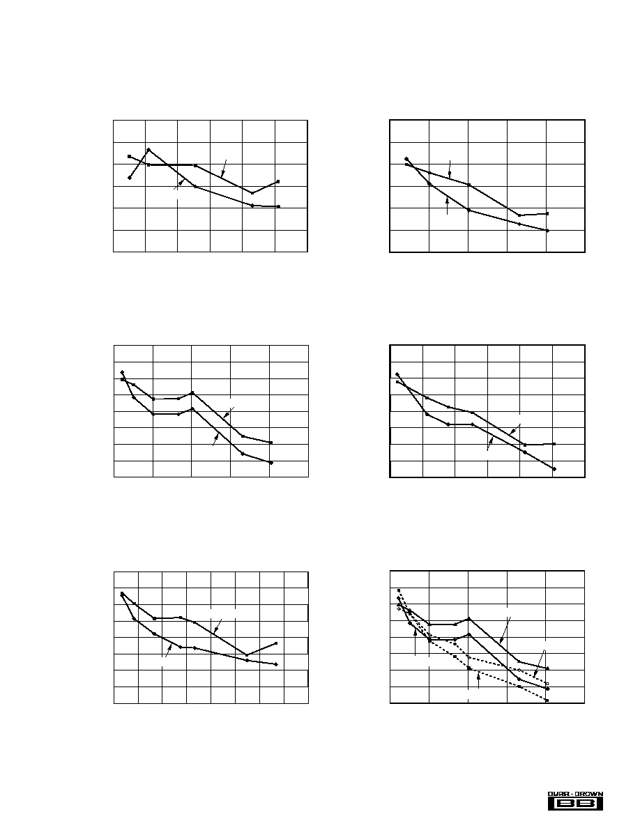
9
TYPICAL PERFORMANCE CURVES, V
D
= V
A
= +3V
At T
A
= +25
∞
C, Differential I
OUT
= 20mA, 50
double-terminated load, SFDR up to Nyquist, unless otherwise specified.
SFDR vs f
OUT
AT 25MSPS (3V)
Frequency (MHz)
SFDR (dBc)
85
80
75
70
65
60
55
2.0
4.0
6.0
8.0
10.0
12.0
0
0dBFS
≠6dBFS
SFDR vs f
OUT
AT 50MSPS (3V)
Frequency (MHz)
SFDR (dBc)
85
80
75
70
65
60
55
5.0
10.0
15.0
20.0
25.0
0
≠6dBFS
0dBFS
DIFFERENTIAL vs SINGLE-ENDED SFDR vs f
OUT
AT 100MSPS (3V)
Frequency (MHz)
SFDR (dBc)
85
80
75
70
65
60
55
50
45
10.0
20.0
30.0
40.0
50.0
0
Diff (0dBFS)
I
OUT
(≠6dBFS)
I
OUT
(0dBFS)
Diff (≠6dBFS)
SFDR vs f
OUT
AT 165MSPS (3V)
Frequency (MHz)
SFDR (dBc)
80
75
70
65
60
55
50
45
40
20.0
10.0
30.0
40.0
50.0
70.0
60.0
80.0
0
≠6dBFS
0dBFS
SFDR vs f
OUT
AT 125MSPS (3V)
Frequency (MHz)
SFDR (dBc)
85
80
75
70
65
60
55
50
45
10.0
20.0
30.0
50.0
40.0
60.0
0
0dBFS
≠6dBFS
SFDR vs f
OUT
AT 100MSPS (3V)
Frequency (MHz)
SFDR (dBc)
85
80
75
70
65
60
55
50
45
10.0
20.0
30.0
40.0
50.0
0
≠6dBFS
0dBFS
Æ
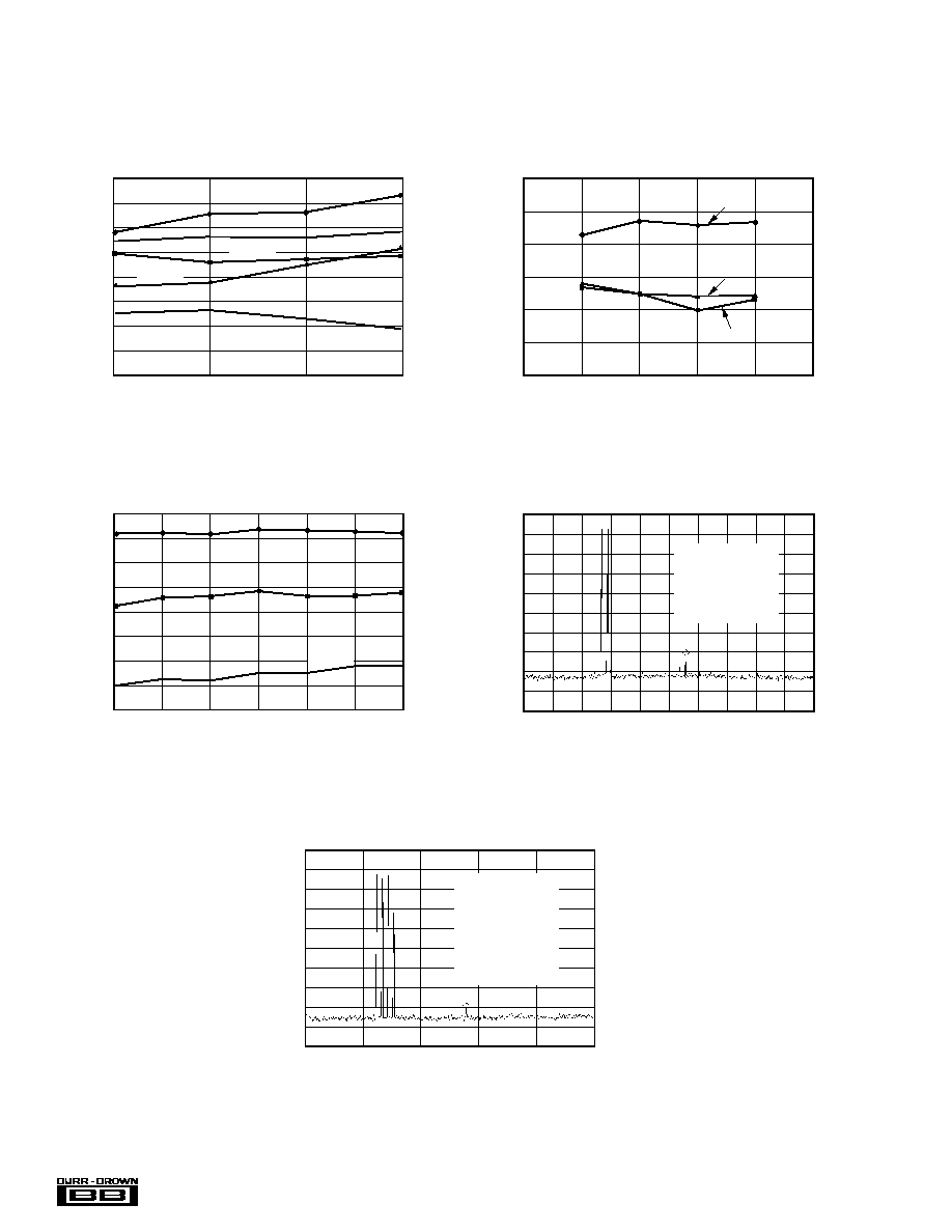
DAC904
10
TYPICAL PERFORMANCE CURVES, V
D
= V
A
= +3V (Cont.)
At T
A
= +25
∞
C, Differential I
OUT
= 20mA, 50
double-terminated load, SFDR up to Nyquist, unless otherwise specified.
DUAL-TONE OUTPUT SPECTRUM (3V)
Frequency (MHz)
Magnitude (dBm)
0
0
≠10
≠20
≠30
≠40
≠50
≠60
≠70
≠80
≠90
≠100
5
10
15
20
25
30
35
40
45
50
f
CLOCK
= 100MSPS
f
OUT1
= 13.5MHz
f
OUT2
= 14.5MHz
SFDR = 64dBc
Amplitude = 0dBFS
FOUR-TONE OUTPUT SPECTRUM (3V)
Frequency (MHz)
Magnitude (dBm)
0
0
≠10
≠20
≠30
≠40
≠50
≠60
≠70
≠80
≠90
≠100
5
10
15
20
25
f
CLOCK
= 50MSPS
f
OUT1
= 6.25MHz
f
OUT2
= 6.75MHz
f
OUT3
= 7.25MHz
f
OUT4
= 7.75MHz
SFDR = 67dBc
Amplitude = 0dBFS
SFDR vs TEMPERATURE AT 100MSPS, 0dBFS (3V)
Temperature (
∞
C)
SFDR (dBc)
80
75
70
65
60
55
50
45
40
≠20
0
25
70
50
85
≠40
2.1MHz
10.1MHz
40.4MHz
X
X
X
X
X
X
X
THD vs f
CLOCK
AT f
OUT
= 2.1MHz (3V)
f
CLOCK
(MSPS)
THD (dBc)
≠70
≠75
≠80
≠85
≠90
≠95
≠100
25
50
100
125
150
0
2HD
4HD
3HD
I
OUTFS
(mA)
SFDR (dBc)
80
75
70
65
60
55
50
45
40
5
10
20
2
X
X
*
*
*
*
X
X
SFDR vs I
OUTFS
and f
OUT
AT 100MSPS (3V)
2.1MHz
5.04MHz
20.2MHz
10.1MHz
40.4MHz

Æ
DAC904
11
APPLICATION INFORMATION
THEORY OF OPERATION
The architecture of the DAC904 uses the current steering
technique to enable fast switching and a high update rate.
The core element within the monolithic D/A converter is an
array of segmented current sources, which are designed to
deliver a full-scale output current of up to 20mA (see
Figure 1). An internal decoder addresses the differential
current switches each time the DAC is updated and a
corresponding output current is formed by steering all
currents to either output summing node, I
OUT
or I
OUT
.
The complementary outputs deliver a differential output
signal, which improves the dynamic performance through
reduction of even-order harmonics, common-mode signals
(noise), and double the peak-to-peak output signal swing by
a factor of two, compared to single-ended operation.
The segmented architecture results in a significant reduc-
tion of the glitch energy, and improves the dynamic perfor-
mance (SFDR) and DNL. The current outputs maintain a
very high output impedance of greater than 200k
.
The full-scale output current is determined by the ratio of
the internal reference voltage (1.24V) and an external
resistor, R
SET
. The resulting I
REF
is internally multiplied by
a factor of 32 to produce an effective DAC output current
that can range from 2mA to 20mA, depending on the value
of R
SET
.
The DAC904 is split into a digital and an analog portion,
each of which is powered through its own supply pin. The
digital section includes edge-triggered input latches and the
decoder logic, while the analog section comprises the cur-
rent source array with its associated switches and the
reference circuitry.
DAC TRANSFER FUNCTION
The total output current, I
OUTFS
, of the DAC904 is the
summation of the two complementary output currents:
I
OUTFS
= I
OUT
+ I
OUT
(1)
The individual output currents depend on the DAC code and
can be expressed as:
I
OUT
= I
OUTFS
∑ (Code/16384)
(2)
I
OUT
= I
OUTFS
∑ (16383 - Code/16384)
(3)
where `Code' is the decimal representation of the DAC data
input word. Additionally, I
OUTFS
is a function of the refer-
ence current I
REF
, which is determined by the reference
voltage and the external setting resistor, R
SET
.
I
OUTFS
= 32 ∑ I
REF
= 32 ∑ V
REF
/R
SET
(4)
In most cases the complementary outputs will drive resistive
loads or a terminated transformer. A signal voltage will
develop at each output according to:
V
OUT
= I
OUT
∑ R
LOAD
(5)
V
OUT
= I
OUT
∑ R
LOAD
(6)
FIGURE 1. Functional Block Diagram of the DAC904.
PMOS
Current
Source
Array
LSB
Switches
Segmented
MSB
Switches
+1.24V Ref
Latches and Switch
Decoder Logic
14-Bit Data Input
D13...D0
DAC904
Full-Scale
Adjust
Resistor
Ref
Control
Amp
Ref
Buffer
BW
+V
D
+V
A
R
SET
2k
CLK
DGND
Ref
Input
0.1
µ
F
INT/EXT
I
OUT
I
OUT
BYP
PD
20pF
50
50
20pF
1:1
V
OUT
0.1
µ
F
400pF
0.1
µ
F
+3V to +5V
Analog
Bandwidth
Control
+3V to +5V
Digital
FSA
REF
IN
AGND
Analog
Ground
Digital
Ground
Power Down
(internal pull-down)
Clock
Input
NOTE: Supply bypassing not shown.

Æ
DAC904
12
The value of the load resistance is limited by the output
compliance specification of the DAC904. To maintain speci-
fied linearity performance, the voltage for I
OUT
and I
OUT
should not exceed the maximum allowable compliance range.
The two single-ended output voltages can be combined to
find the total differential output swing:
(7)
ANALOG OUTPUTS
The DAC904 provides two complementary current outputs,
I
OUT
and I
OUT
. The simplified circuit of the analog output
stage representing the differential topology is shown in
Figure 2. The output impedance of 200k
|| 12pF for I
OUT
and I
OUT
results from the parallel combination of the differ-
ential switches, along with the current sources and associ-
ated parasitic capacitances.
I
OUT
and I
OUT
. Furthermore, using the differential output
configuration in combination with a transformer will be
instrumental for achieving excellent distortion performance.
Common-mode errors, such as even-order harmonics or
noise, can be substantially reduced. This is particularly the
case with high output frequencies and/or output amplitudes
below full-scale.
For those applications requiring the optimum distortion and
noise performance, it is recommended to select a full-scale
output of 20mA. A lower full-scale range down to 2mA may
be considered for applications that require a low power
consumption, but can tolerate a reduced performance level.
FIGURE 2. Equivalent Analog Output.
The signal voltage swing that may develop at the two
outputs, I
OUT
and I
OUT
, is limited by a negative and positive
compliance. The negative limit of ≠1V is given by the
breakdown voltage of the CMOS process, and exceeding it
will compromise the reliability of the DAC904, or even
cause permanent damage. With the full-scale output set to
20mA, the positive compliance equals 1.25V, operating with
+V
D
= 5V. Note that the compliance range decreases to
about 1V for a selected output current of I
OUTFS
= 2mA.
Care should be taken that the configuration of DAC904 does
not exceed the compliance range to avoid degradation of the
distortion performance and integral linearity.
Best distortion performance is typically achieved with the
maximum full-scale output signal limited to approximately
0.5V. This is the case for a 50
doubly terminated load and
a 20mA full-scale output current. A variety of loads can be
adapted to the output of the DAC904 by selecting a suitable
transformer while maintaining optimum voltage levels at
OUTPUT CONFIGURATIONS
The current output of the DAC904 allows for a variety of
configurations, some of which are illustrated below. As
mentioned previously, utilizing the converter's differential
outputs will yield the best dynamic performance. Such a
differential output circuit may consist of an RF transformer
(see Figure 3) or a differential amplifier configuration (see
Figure 4). The transformer configuration is ideal for most
applications with ac coupling, while op amps will be suitable
for a dc-coupled configuration.
The single-ended configuration (see Figure 6) may be con-
sidered for applications requiring a unipolar output voltage.
Connecting a resistor from either one of the outputs to
ground will convert the output current into a ground-refer-
enced voltage signal. To improve on the dc linearity an I to
V converter can be used instead. This will result in a
negative signal excursion and, therefore, requires a dual
supply amplifier.
DIFFERENTIAL WITH TRANSFORMER
Using an RF transformer provides a convenient way of
converting the differential output signal into a single-ended
signal while achieving excellent dynamic performance (see
Figure 3). The appropriate transformer should be carefully
selected based on the output frequency spectrum and imped-
ance requirements. The differential transformer configura-
tion has the benefit of significantly reducing common-mode
signals, thus improving the dynamic performance over a
wide range of frequencies. Furthermore, by selecting a
suitable impedance ratio (winding ratio), the transformer can
be used to provide optimum impedance matching while
controlling the compliance voltage for the converter outputs.
The model shown, ADT1-1WT (by Mini-Circuits), has a 1:1
ratio and may be used to interface the DAC904 to a 50
load. This results in a 25
load for each of the outputs, I
OUT
and I
OUT
. The output signals are ac coupled and inherently
isolated because of the transformer's magnetic coupling .
INPUT CODE (D13 - D0)
I
OUT
I
OUT
11 1111 1111 1111
20mA
0mA
10 0000 0000 0000
10mA
10mA
00 0000 0000 0000
0mA
20mA
Table I. Input Coding vs Analog Output Current.
V
V
V
Code
I
R
OUTDIFF
OUT
OUT
OUTFS
LOAD
=
= ∑
∑
∑
≠
(
≠
)
2
16383
16384
I
OUT
I
OUT
DAC904
R
L
R
L
+V
A

Æ
DAC904
13
FIGURE 4. Difference Amplifier Provides Differential to
Single-Ended Conversion and AC-Coupling.
FIGURE 5. Dual, Voltage-Feedback Amplifier OPA2680
Forms Differential Transimpedance Amplifier.
As shown in Figure 3, the transformer's center tap is con-
nected to ground. This forces the voltage swing on I
OUT
and
I
OUT
to be centered at 0V. In this case the two resistors, R
S
,
may be replaced with one, R
DIFF
, or omitted altogether. This
approach should only be used if all components are close to
each other, and if the VSWR is not important. A complete
power transfer from the DAC output to the load can be
realized, but the output compliance range should be ob-
served. Alternatively, if the center tap is not connected, the
signal swing will be centered at R
S
∑ I
OUTFS
/2. However, in
this case, the two resistors, R
S
, must be used to enable the
necessary dc-current flow for both outputs.
DIFFERENTIAL CONFIGURATION USING AN OP AMP
If the application requires a dc-coupled output, a difference
amplifier may be considered, as shown in Figure 4. Four
external resistors are needed to configure the voltage-feed-
back op amp OPA680 as a difference amplifier performing
the differential to single-ended conversion. Under the shown
configuration, the DAC904 generates a differential output
signal of 0.5Vp-p at the load resistors, R
L
. The resistor
values shown were selected to result in a symmetric 25
loading for each of the current outputs since the input
impedance of the difference amplifier is in parallel to resis-
tors R
L
, and should be considered.
The OPA680 is configured for a gain of two. Therefore,
operating the DAC904 with a 20mA full-scale output will
produce a voltage output of
±
1V. This requires the amplifier
to operate off of a dual power supply (
±
5V). The tolerance
of the resistors typically sets the limit for the achievable
common-mode rejection. An improvement can be obtained
by fine tuning resistor R
4
.
This configuration typically delivers a lower level of ac
performance than the previously discussed transformer solu-
tion because the amplifier introduces another source of
distortion. Suitable amplifiers should be selected based on
their slew-rate, harmonic distortion, and output swing capa-
bilities. High-speed amplifiers like the OPA680 or OPA687
may be considered. The ac performance of this circuit may
be improved by adding a small capacitor, C
DIFF
, between the
outputs I
OUT
and I
OUT
, as shown in Figure 4. This will intro-
duce a real pole to create a low-pass filter in order to slew-
limit the DACs fast output signal steps, which otherwise
could drive the amplifier into slew-limitations or into an
overload condition; both would cause excessive distortion.
The difference amplifier can easily be modified to add a
level shift for applications requiring the single-ended output
voltage to be unipolar, i.e., swing between 0V and +2V.
DUAL TRANSIMPEDANCE OUTPUT CONFIGURATION
The circuit example of Figure 5 shows the signal output
currents connected into the summing junction of the
OPA2680, which is set up as a transimpedance stage, or
`I to V converter'. With this circuit, the DAC's output will
be kept at a virtual ground, minimizing the effects of output
impedance variations, and resulting in the best dc linearity
(INL). However, as mentioned previously, the amplifier
may be driven into slew-rate limitations, and produce un-
wanted distortion. This may occur, especially, at high DAC
update rates.
I
OUT
I
OUT
DAC904
R
L
26.1
R
L
28.7
R
4
402
R
3
200
R
2
402
R
1
200
OPA680
C
DIFF
+5V
V
OUT
≠5V
1/2
OPA2680
1/2
OPA2680
DAC904
≠V
OUT
= I
OUT
∑ R
F
≠V
OUT
= I
OUT
∑ R
F
R
F1
R
F2
C
F1
C
F2
C
D1
C
D2
I
OUT
I
OUT
50
50
≠5V
+5V
FIGURE 3. Differential Output Configuration Using an RF
Transformer.
I
OUT
I
OUT
DAC904
1:1
ADT1-1WT
(Mini-Circuits)
R
S
50
R
S
50
R
L
Optional
R
DIFF
Æ
DAC904
14
FIGURE 6. Driving a Doubly Terminated 50
Cable Directly.
FIGURE 7. Internal Reference Configuration.
The DC gain for this circuit is equal to feedback resistor R
F
.
At high frequencies, the DAC output impedance (C
D1
, C
D2
)
will produce a zero in the noise gain for the OPA2680 that
may cause peaking in the closed-loop frequency response.
C
F
is added across R
F
to compensate for this noise gain
peaking. To achieve a flat transimpedance frequency re-
sponse, the pole in each feedback network should be set to:
1
2
4
R C
GBP
R C
F
F
F
D
=
(8)
with GBP = Gain Bandwidth Product of OPA
which will give a corner frequency f
-3dB
of approximately:
f
GBP
R C
dB
F
D
-
=
3
2
(9)
The full-scale output voltage is defined by the product of
I
OUTFS
∑ R
F
, and has a negative unipolar excursion. To
improve on the ac performance of this circuit, adjustment of
R
F
and/or I
OUTFS
should be considered. Further extensions of
this application example may include adding a differential
filter at the OPA2680's output followed by a transformer, in
order to convert to a single-ended signal.
SINGLE-ENDED CONFIGURATION
Using a single load resistor connected to the one of the DAC
outputs, a simple current-to-voltage conversion can be ac-
complished. The circuit in Figure 6 shows a 50
resistor
connected to I
OUT
, providing the termination of the further
connected 50
cable. Therefore, with a nominal output
current of 20mA, the DAC produces a total signal swing of
0 to 0.5V into the 25
load.
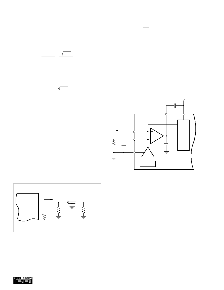
INTERNAL REFERENCE OPERATION
The DAC904 has an on-chip reference circuit which com-
prises a 1.24V bandgap reference and a control amplifier.
Grounding of pin 16, INT/EXT, enables the internal refer-
ence operation. The full-scale output current, I
OUTFS
, of the
DAC904 is determined by the reference voltage, V
REF
, and
the value of resistor R
SET
. I
OUTFS
can be calculated by:
I
OUTFS
= 32 ∑ I
REF
= 32 ∑ V
REF
/ R
SET
(10)
As shown in Figure 7, the external resistor R
SET
connects to
the FSA pin (Full-Scale Adjust). The reference control
amplifier operates as a V to I converter producing a refer-
ence current, I
REF
, which is determined by the ratio of V
REF
and R
SET
(see Equation 10). The full-scale output current,
I
OUTFS
, results from multiplying I
REF
by a fixed factor of 32.
Different load resistor values may be selected as long as the
output compliance range is not exceeded. Additionally, the
output current, I
OUTFS
, and the load resistor, may be mutu-
ally adjusted to provide the desired output signal swing and
performance.
Using the internal reference, a 2k
resistor value results in
a 20mA full-scale output. Resistors with a tolerance of 1%
or better should be considered. Selecting higher values, the
converter output can be adjusted from 20mA down to 2mA.
Operating the DAC904 at lower than 20mA output currents
may be desirable for reasons of reducing the total power
consumption, improving the distortion performance, or ob-
serving the output compliance voltage limitations for a given
load condition.
It is recommended to bypass the REF
IN
pin with a ceramic chip
capacitor of 0.1
µ
F or more. The control amplifier is internally
compensated, and its small signal bandwidth is approximately
1.3MHz. To improve the ac performance, an additional capaci-
tor (C
COMPEXT
) should be applied between the BW pin and the
analog supply, +V
A
, as shown in Figure 7. Using a 0.1
µ
F
capacitor, the small-signal bandwidth and output impedance of
the control amplifier is further diminished, reducing the noise
that is fed into the current source array. This also helps
shunting feedthrough signals more effectively, and improving
the noise performance of the DAC904.
I
OUT
I
OUT
DAC904
25
50
50
I
OUTFS
= 20mA
V
OUT
= 0V to +0.5V
DAC904
C
COMPEXT
0.1
µ
F
C
COMP
400pF
+1.24V Ref.
R
SET
2k
0.1
µ
F
INT/EXT
FSA
BW
+5V
+V
A
REF
IN
Current
Sources
I
REF
=
V
REF
R
SET
Ref
Control
Amp
Æ
DAC904
15
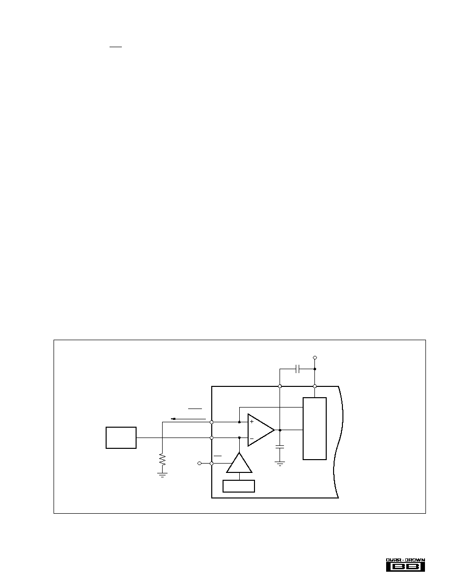
FIGURE 8. External Reference Configuration.
EXTERNAL REFERENCE OPERATION
The internal reference can be disabled by applying a logic
High (+V
A
) to pin INT/EXT. An external reference voltage
can then be driven into the REF
IN
pin, which in this case
functions as an input, as shown in Figure 8. The use of an
external reference may be considered for applications that
require higher accuracy and drift performance, or to add the
ability of dynamic gain control.
While a 0.1
µ
F capacitor is recommended to be used with the
internal reference, it is optional for the external reference
operation. The reference input, REF
IN
, has a high input
impedance (1M
) and can easily be driven by various
sources. Note that the voltage range of the external reference
should stay within the compliance range of the reference
input (0.1V to 1.25V).
DIGITAL INPUTS
The digital inputs, D0 (LSB) through D13 (MSB) of the
DAC904 accept standard positive binary coding. The digital
input word is latched into a master-slave latch with the rising
edge of the clock. The DAC output becomes updated with
the following rising clock edge (refer to the specification
table and timing diagram for details). The best performance
will be achieved with a 50% clock duty cycle, however, the
duty cycle may vary as long as the timing specifications are
met. Additionally, the setup and hold times may be chosen
within their specified limits.
All digital inputs are CMOS compatible. The logic thresh-
olds depend on the applied digital supply voltage such that
they are set to approximately half the supply voltage;
Vth = +VD/2 (
±
20% tolerance). The DAC904 is designed to
operate over a supply range of 2.7V to 5.5V.
POWER-DOWN MODE
The DAC904 features a power-down function which can be
used to reduce the supply current to less than 9mA over the
specified supply range of 2.7V to 5.5V. Applying a logic
High to the PD pin will initiate the power-down mode, while
a logic Low enables normal operation. When left uncon-
nected, an internal active pull-down circuit will enable the
normal operation of the converter.
GROUNDING, DECOUPLING AND
LAYOUT INFORMATION
Proper grounding and bypassing, short lead length, and the
use of ground planes are particularly important for high
frequency designs. Multilayer pc-boards are recommended
for best performance since they offer distinct advantages
such as minimization of ground impedance, separation of
signal layers by ground layers, etc.
The DAC904 uses separate pins for its analog and digital
supply and ground connections. The placement of the decou-
pling capacitor should be such that the analog supply (+V
A
)
is bypassed to the analog ground (AGND), and the digital
supply bypassed to the digital ground (DGND). In most
cases 0.1uF ceramic chip capacitors at each supply pin are
adequate to provide a low impedance decoupling path. Keep
in mind that their effectiveness largely depends on the
proximity to the individual supply and ground pins. There-
fore they should be located as close as physically possible to
those device leads. Whenever possible, the capacitors should
be located immediately under each pair of supply/ground
pins on the reverse side of the pc board. This layout ap-
proach will minimize the parasitic inductance of component
leads and pcb runs.
R
SET
+5V
External
Reference
I
REF
=
V
REF
R
SET
DAC904
C
COMPEXT
0.1
µ
F
C
COMP
400pF
+1.24V Ref.
INT/EXT
FSA
BW
+5V
+V
A
REF
IN
Current
Sources
Ref
Control
Amp

Æ
DAC904
16
Further supply decoupling with surface mount tantalum
capacitors (1uF to 4.7uF) may be added as needed in
proximity of the converter.
Low noise is required for all supply and ground connections
to the DAC904. It is recommended to use a multilayer pc-
board utilizing separate power and ground planes. Mixed
signal designs require particular attention to the routing of
the different supply currents and signal traces. Generally,
analog supply and ground planes should only extend into
analog signal areas, such as the DAC output signal and the
reference signal. Digital supply and ground planes must be
confined to areas covering digital circuitry, including the
digital input lines connecting to the converter, as well as the
clock signal. The analog and digital ground planes should be
joined together at one point underneath the D/A converter.
This can be realized with a short track of approximately
1/8inch (3mm).
The power to the DAC904 should be provided through the
use of wide pcb runs or planes. Wide runs will present a
lower trace impedance, further optimizing the supply decou-
pling. The analog and digital supplies for the converter
should only be connected together at the supply connector of
the pc board. In the case of only one supply voltage being
available to power the DAC, ferrite beads along with bypass
capacitors may be used to create an LC filter. This will
generate a low noise analog supply voltage, which can then
be connected to the +V
A
supply pin of the DAC904.
While designing the layout, it is important to keep the analog
signal traces separated from any digital line, in order to
prevent noise coupling onto the analog signal path.