 | ÐлекÑÑоннÑй компоненÑ: DCP02 | СкаÑаÑÑ:  PDF PDF  ZIP ZIP |
DCP02
®
Miniature, 2W Isolated
UNREGULATED DC/DC CONVERTERS
©
1999 Burr-Brown Corporation
PDS-1558A
Printed in U.S.A. December, 1999
DCP02
Series
International Airport Industrial Park · Mailing Address: PO Box 11400, Tucson, AZ 85734 · Street Address: 6730 S. Tucson Blvd., Tucson, AZ 85706 · Tel: (520) 746-1111
Twx: 910-952-1111 · Internet: http://www.burr-brown.com/ · Cable: BBRCORP · Telex: 066-6491 · FAX: (520) 889-1510 · Immediate Product Info: (800) 548-6132
For most current data sheet and other
product information, visit www.burr-brown.com
FEATURES
q
UP TO 89% EFFICIENCY
q
THERMAL PROTECTION
q
DEVICE-TO-DEVICE SYNCHRONIZATION
q
SO-28
(1)
POWER DENSITY OF 106W/in
3
(6.5W/cm
3
)
q
EN55022 CLASS B EMC PERFORMANCE
q
UL1950 RECOGNIZED
q
JEDEC 14-PIN AND SO-28
(1)
PACKAGES
DESCRIPTION
The DCP02 series is a family of 2W, unregulated,
isolated DC/DC converters. Requiring a minimum of
external components and including on-chip device
protection, the DCP02 series provides extra features
such as output disable and synchronization of switch-
ing frequencies.
The use of a highly integrated package design results
in highly reliable products with power densities of
79W/in
3
(4.8W/cm
3
) for the 14-PDIP, and 106W/in
3
(6.5W/cm
3
) for the SO-28
(1)
. This combination of
features and small size makes the DCP02 suitable for
a wide range of applications.
NOTE: (1) SO-28 version available January, 2000.
APPLICATIONS
q
POINT-OF-USE POWER CONVERSION
q
GROUND LOOP ELIMINATION
q
DATA ACQUISITION
q
INDUSTRIAL CONTROL AND
INSTRUMENTATION
q
TEST EQUIPMENT
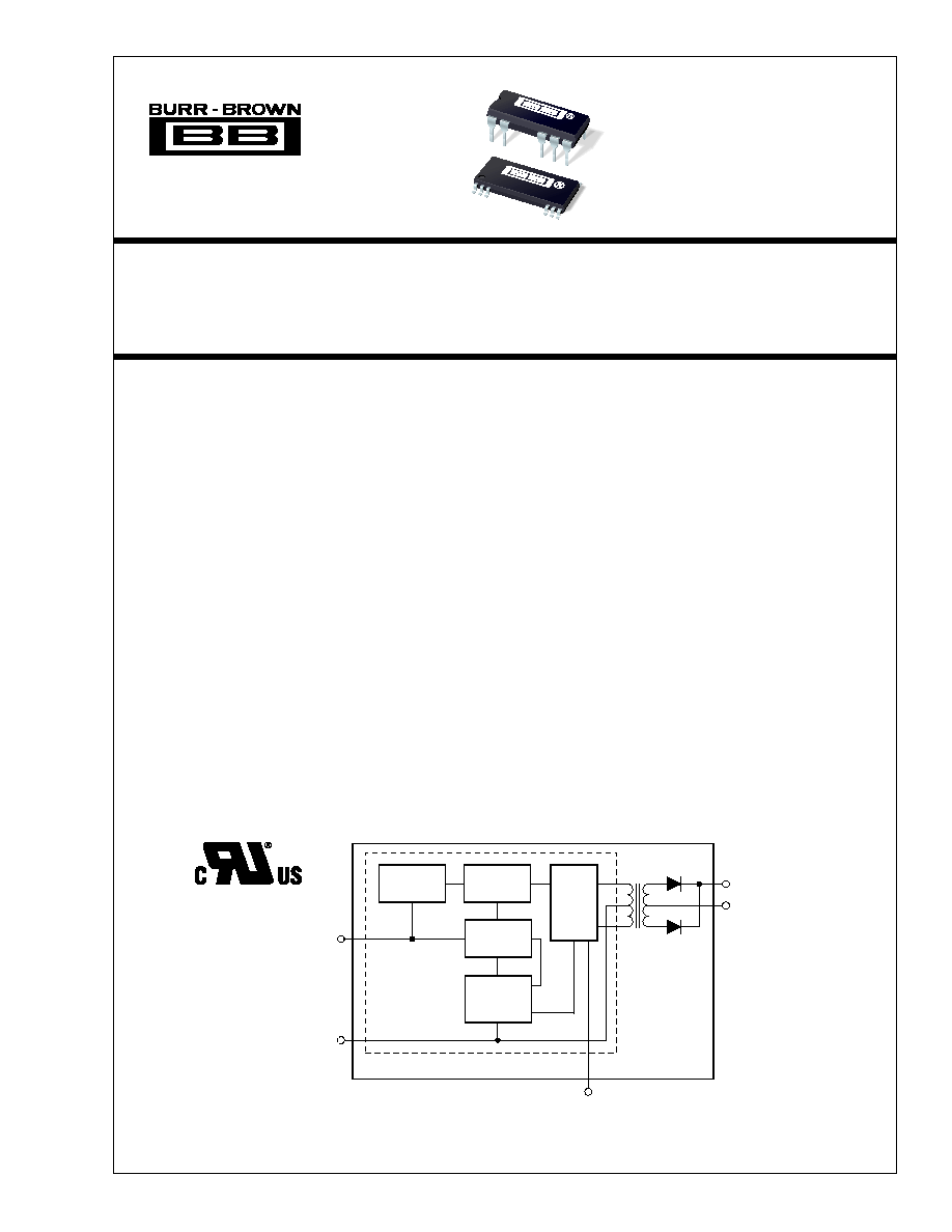
I
BIAS
Power
Stage
V
OUT
÷
2
Reset
800kHz
Oscillator
Watch-dog/
start-up
PSU
Thermal
Shutdown
SYNC/DISABLE
V
S
0V
Power Controller IC
0V
DCP02
DCP02
2
DCP02
®
INPUT
OUTPUT
LOAD
NO LOAD
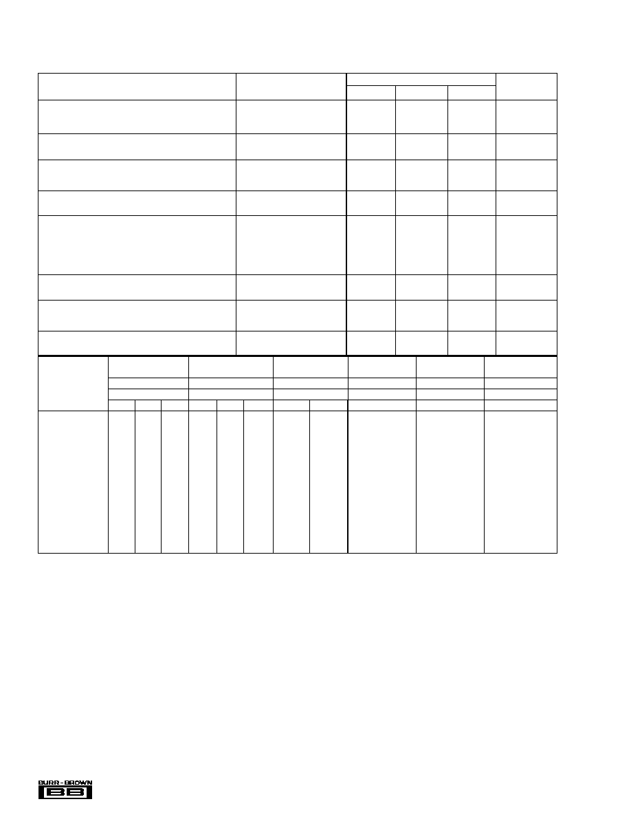
BARRIER
VOLTAGE (V)
VOLTAGE (V)
REGULATION (%)
CURRENT (mA)
EFFICIENCY (%)
CAPACITANCE (pF)
V
S
V
NOM
I
Q
C
ISO
75% LOAD
(2)
10% TO 100% LOAD
0% LOAD
100% LOAD
V
ISO
= 750V
RMS
PRODUCT
MIN
TYP
MAX
MIN
TYP
MAX
TYP
MAX
TYP
TYP
TYP
DCP020503P
(3)
, U
(3)
4.5
5
5.5
3.13
3.3
3.46
19
30
18
74
26
DCP020505P, U
(4)
4.5
5
5.5
4.75
5
5.25
14
20
18
80
22
DCP020507P, U
(4)
4.5
5
5.5
6.65
7
7.35
14
25
20
81
30
DCP020509P, U
(4)
4.5
5
5.5
8.55
9
9.45
12
20
23
82
31
DCP020515DP, U
(4)
4.5
5
5.5
±
14.25
±
15
±
15.75
11
20
27
85
24
DCP021205P, U
(4)
10.8
12
13.2
4.75
5
5.25
7
15
14
83
33
DCP021212P
10.8
12
13.2
11.4
12
12.6
7
20
15
87
47
DCP021212DP
10.8
12
13.2
±
11.4
±
12
±
12.6
6
20
16
88
35
DCP021515P
13.5
15
16.5
14.25
15
15.75
6
20
15
88
42
DCP022405P
21.6
24
26.4
4.85
5
5.35
6
10
13
81
33
DCP022405DP
21.6
24
26.4
±
4.75
±
5
±
5.25
6
15
12
80
22
DCP022415DP
21.6
24
26.4
±
14.25
±
15
±
15.75
6
20
16
79
44
NOTES: (1) During UL1950 recognition tests only. (2) 100% Load Current = 2W/V
NOM
TYP. (3) DCP020503P and U models available January, 2000.
(4) SO-28 version available January, 2000.
The information provided herein is believed to be reliable; however, BURR-BROWN assumes no responsibility for inaccuracies or omissions. BURR-BROWN assumes
no responsibility for the use of this information, and all use of such information shall be entirely at the user's own risk. Prices and specifications are subject to change
without notice. No patent rights or licenses to any of the circuits described herein are implied or granted to any third party. BURR-BROWN does not authorize or warrant
any BURR-BROWN product for use in life support devices and/or systems.
SPECIFICATIONS
At T
A
= +25
°
C, unless otherwise specified.
DCP02 SERIES
PARAMETER
CONDITIONS
MIN
TYP
MAX
UNITS
OUTPUT
Power
100% Full Load
2
W
Ripple
O/P Capacitor = 1
µ
F, 50% Load
20
mVp-p
INPUT
Voltage Range on V
S
10
10
%
ISOLATION
Voltage
1s Flash Test
1
kVrms
60s Test, UL1950
(1)
1
kVrms
LINE
Regulation
1
%/1% of V
S
SWITCHING/SYNCHRONIZATION
Oscillator Frequency (f
OSC
)
Switching Frequency = f
OSC
/2
800
kHz
Sync Input Low
0
0.4
V
Sync Input Current
V
SYNC
= +2V
75
µ
A
Disable Time
2
µ
s
Capacitance Loading on Sync Pin
External
10
pF
RELIABILITY
Demonstrated
T
A
= +55
°
C
75
FITS
THERMAL SHUTDOWN
IC Temperature at Shutdown
150
°
C
Shutdown Current
3
mA
TEMPERATURE RANGE
Operating
40
+85
°
C
3
®
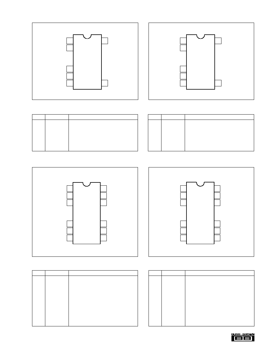
DCP02
Top View
SOIC
PIN CONFIGURATION (Single-SOIC)
(1)
Top View
SOIC
PIN CONFIGURATION (Dual-SOIC)
(1)
PIN DEFINITION (Single-SOIC)
(1)
PIN #
PIN NAME
DESCRIPTION
1
V
S
Voltage Input
2
0V
Input Side Common
3
0V
Input Side Common
12
0V
Output Side Common
13
+V
OUT
+Voltage Out
14
NC
Not Connected
15
NC
Not Connected
16
NC
Not Connected
17
NC
Not Connected
26
NC
Not Connected
27
NC
Not Connected
28
SYNC
Synchronization Pin
PIN DEFINITION (Dual-SOIC)
(1)
DCP02
1
2
3
12
13
14
28
27
26
17
16
15
V
S
0V
0V
0V
+V
OUT
NC
SYNC
NC
NC
NC
NC
NC
DCP02
1
2
3
12
13
14
28
27
26
17
16
15
V
S
0V
0V
0V
+V
OUT
V
OUT
SYNC
NC
NC
NC
NC
NC
PIN #
PIN NAME
DESCRIPTION
1
V
S
Voltage Input
2
0V
Input Side Common
3
0V
Input Side Common
12
0V
Output Side Common
13
+V
OUT
+Voltage Out
14
V
OUT
Voltage Out
15
NC
Not Connected
16
NC
Not Connected
17
NC
Not Connected
26
NC
Not Connected
27
NC
Not Connected
28
SYNC
Synchronization Pin
Top View
DIP
PIN CONFIGURATION (Single-DIP)
Top View
DIP
PIN CONFIGURATION (Dual-DIP)
PIN DEFINITION (Single-DIP)
PIN #
PIN NAME
DESCRIPTION
1
V
S
Voltage Input
2
0V
Input Side Common
5
0V
Output Side Common
6
+V
OUT
+Voltage Out
7
NC
Not Connected
8
NC
Not Connected
14
SYNC
Synchronization Pin
PIN DEFINITION (Dual-DIP)
PIN #
PIN NAME
DESCRIPTION
1
V
S
Voltage Input
2
0V
Input Side Common
5
0V
Output Side Common
6
+V
OUT
+Voltage Out
7
V
OUT
Voltage Out
8
NC
Not Connected
14
SYNC
Synchronization Pin
DCP02
1
2
5
6
7
14
8
V
S
0V
0V
+V
OUT
NC
SYNC
NC
DCP02
1
2
5
6
7
14
8
V
S
0V
0V
+V
OUT
V
OUT
SYNC
NC
NOTE: (1) SO-28 version available January, 2000.
4
DCP02
®
ELECTROSTATIC
DISCHARGE SENSITIVITY
This integrated circuit can be damaged by ESD. Burr-Brown
recommends that all integrated circuits be handled with
appropriate precautions. Failure to observe proper handling
and installation procedures can cause damage.
ESD damage can range from subtle performance degrada-
tion to complete device failure. Precision integrated circuits
may be more susceptible to damage because very small
parametric changes could cause the device not to meet its
published specifications.
Input Voltage
5V Input Models .................................................................................. 7V
12V Input Models .............................................................................. 15V
15V Input Models .............................................................................. 18V
24V Input Models .............................................................................. 29V
Storage Temperature ...................................................... 60
°
C to +125
°
C
Lead Temperature (soldering, 10s) ................................................. 270
°
C
ABSOLUTE MAXIMUM RATINGS
DCP02
Basic Model Number: 2W Product
Voltage Input:
5V In
Voltage Output:
5V Out
Dual Output:
Package Code:
P = 14-Pin Plastic DIP
U = 28-Lead SOIC
(1)
NOTE: (1) SO-28 version available 1Q00.
ORDERING INFORMATION
05
05
(
)
( D )
PACKAGE
SPECIFIED
DRAWING
TEMPERATURE
PACKAGE
ORDERING
TRANSPORT
PRODUCT
PACKAGE
NUMBER
RANGE
MARKING
NUMBER
(1)
MEDIA
Single
DCP020503P
(2)
DIP-14
010-1
40
°
C to +85
°
C
DCP020503P
DCP020503P
Rails
DCP020503U
(2)
SOIC-28
217-2
40
°
C to +85
°
C
DCP020503U
DCP020503U/1K
Tape and Reels
DCP020505P
DIP-14
010-1
40
°
C to +85
°
C
DCP020505P
DCP020505P
Rails
DCP020505U
(2)
SOIC-28
217-2
40
°
C to +85
°
C
DCP020505U
DCP020505U/1K
Tape and Reels
DCP020507P
DIP-14
010-1
40
°
C to +85
°
C
DCP020507P
DCP020507P
Rails
DCP020507U
(2)
SOIC-28
217-2
40
°
C to +85
°
C
DCP020507U
DCP020507U/1K
Tape and Reels
DCP020509P
DIP-14
010-1
40
°
C to +85
°
C
DCP020509P
DCP020509P
Rails
DCP020509U
(2)
SOIC-28
217-2
40
°
C to +85
°
C
DCP020509U
DCP020509U/1K
Tape and Reels
DCP021205P
DIP-14
010-1
40
°
C to +85
°
C
DCP021205P
DCP021205P
Rails
DCP021205U
(2)
SOIC-28
217-2
40
°
C to +85
°
C
DCP021205U
DCP021205U/1K
Tape and Reels
DCP021212P
DIP-14
010-1
40
°
C to +85
°
C
DCP021212P
DCP021212P
Rails
DCP021515P
DIP-14
010-1
40
°
C to +85
°
C
DCP021515P
DCP021515P
Rails
DCP022405P
DIP-14
010-1
40
°
C to +85
°
C
DCP022405P
DCP022405P
Rails
Dual
DCP020515DP
DIP-14
010-1
40
°
C to +85
°
C
DCP020515DP
DCP020515DP
Rails
DCP020515DU
(2)
SOIC-28
217-2
40
°
C to +85
°
C
DCP020515DU
DCP020515DU/1K
Tape and Reels
DCP021212DP
DIP-14
010-1
40
°
C to +85
°
C
DCP021212DP
DCP021212DP
Rails
DCP022405DP
DIP-14
010-1
40
°
C to +85
°
C
DCP022405DP
DCP022405DP
Rails
DCP022415DP
DIP-14
010-1
40
°
C to +85
°
C
DCP022415DP
DCP022415DP
Rails
NOTES: (1) Models with a slash (/) are available only in Tape and Reel in the quantities indicated (e.g., /1K indicates 1000 devices per reel). Ordering 1000
pieces of "DCP020503U/1K" will get a single 1000-piece Tape and Reel. (2) Shaded models available January, 2000.
PACKAGE/ORDERING INFORMATION
5
®
DCP02
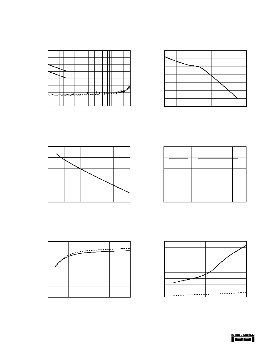
TYPICAL PERFORMANCE CURVES
At T
A
= +25
°
C, unless otherwise noted.
DCP020505P
V
OUT
vs TEMPERATURE (75% Load)
Temperature (
°
C)
V
OUT
(V)
5.04
5.02
5.00
4.98
4.96
4.94
4.92
4.90
20
20
40
60
80
100
0
40
DCP021205P
V
OUT
vs LOAD
5.4
5.3
5.2
5.1
5.0
4.9
Load (%)
V
OUT
(V)
0
20
40
60
80
100
DCP021205P
POWER OUT vs TEMPERATURE (400mA Load)
Temperature (
°
C)
P
OUT
(W)
0
25
50
75
100
25
50
2.5
2.0
1.5
1.0
0.5
0
DCP0212
EFFICIENCY vs LOAD
100
80
60
40
20
0
Load (%)
Ef
ficiency (%)
0
25
50
75
100
DCP1212DP
DCP1205P
DCP020505P
OUTPUT AC RIPPLE (20MHz Band)
450
400
350
300
250
200
150
100
50
0
Load Current (mA)
Ripple (mVp-p)
0
200
0.1
µ
F
400
1
µ
F
DCP020505P
CONDUCTED EMISSIONS (500mA Load)
Emission Level, Peak (dB
µ
A)
Frequency (MHz)
1
0.15
10
30
60
50
40
30
20
10
0
10
20
6
DCP02
®
FIGURE 1. Connecting the DCP02 in Series.
DCP
02
V
OUT 1
V
SUPPLY
V
S
0V
DCP
02
V
OUT 2
V
OUT1
+ V
OUT 2
SYNC
SYNC
V
S
0V
0V
0V
COM
FUNCTIONAL DESCRIPTION
OVERVIEW
The DCP02 offers up to 2W of unregulated output power
from a 5V, 12V, 15V, or 24V input source with a typical
efficiency of up to 89%. This is achieved through highly
integrated packaging technology and the implementation of
a custom power stage and control IC. The circuit design
utilizes an advanced BiCMOS/DMOS process.
POWER STAGE
This uses a push-pull, center-tapped topology switching at
400kHz (divide by 2 from 800kHz oscillator).
OSCILLATOR AND WATCHDOG
The onboard 800kHz oscillator generates the switching
frequency via a divide by 2 circuit. The oscillator can be
synchronized to other DCP02 circuits or an external source,
and is used to minimize system noise.
A watchdog circuit checks the operation of the oscillator
circuit. The oscillator can be stopped by pulling the SYNC
pin LOW. The output pins will be tri-stated. This will occur
in 2
µ
s.
THERMAL SHUTDOWN
The DCP02 is protected by a thermal shutdown circuit. If the
on-chip temperature exceeds 150
°
C, the device will shut
down. Once the temperature falls below 150
°
C, normal
operation will resume.
SYNCHRONIZATION
In the event that more than one DC/DC converter is needed
onboard, beat frequencies and other electrical interference
can be generated. This is due to the variation in switching
frequencies between the DC/DC converters.
The DCP02 overcomes this by allowing devices to be syn-
chronized to one another. Up to eight devices can be syn-
chronized by connecting the SYNC pins together, taking
care to minimize the capacitance of tracking. Significant
stray capacitance (> 10pF) will have the effect of reducing
the switching frequency, or even stopping the oscillator
circuit. It is also recommended that power and ground lines
are star connected.
If synchronized devices are used, it should be noted that, at
start up, all devices will draw maximum current simulta-
neously. This can cause the input voltage to dip and should
it dip below the minimum input voltage (4.5V), the devices
may not start up. A 2.2
µ
F capacitor should be connected
close to the input pins.
If more than eight devices are to be synchronized, it is
recommended that the SYNC pins are driven by an external
device. Details are contained in a separate applications
bulletin (AB-153).
CONSTRUCTION
The DCP02's basic construction is the same as standard ICs.
There is no substrate within the molded package. The
DCP02 is constructed using an IC, rectifier diodes, and a
wound magnetic toroid on a leadframe. As there is no solder
within the package, the DCP02 does not require any special
PCB assembly processing. This results in an isolated
DC/DC converter with inherently high reliability.
7
®
DCP02
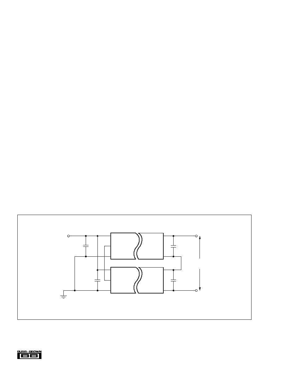
FIGURE 2. Connecting Dual Outputs in Series.
ADDITIONAL FUNCTIONS
DISABLE/ENABLE
The DCP02 can be disabled or enabled by driving the SYNC
pin using an open drain CMOS gate. If the SYNC pin is
pulled low, the DCP02 will be disabled. The disable time
depends upon the external loading; the internal disable func-
tion is implemented in 2
µ
s. Removal of the pull down will
cause the DCP02 to be enabled.
Capacitive loading on the SYNC pin should be minimized in
order to prevent a reduction in the oscillator frequency.
DECOUPLING
Ripple Reduction
The high switching frequency of 400kHz allows simple
filtering. To reduce ripple, it is recommended that a 1
µ
F
capacitor is used on V
OUT
. Dual outputs should both be
decoupled to pin 5. A 2.2
µ
F capacitor on the input is
recommended.
Connecting the DCP02 in Series
Multiple DCP02 isolated 2W DC/DC converters can be
connected in series to provide nonstandard voltage rails.
This is possible by utilizing the floating outputs provided by
the DCP02's galvanic isolation.
Connect the positive V
OUT
from one DCP02 to the negative
V
OUT
(0V) of another (see Figure 1). If the SYNC pins are
tied together, the self-synchronization feature of the DCP02
will prevent beat frequencies on the voltage rails. The SYNC
feature of the DCP02 allows easy series connection without
external filtering, minimizing cost.
The outputs on dual output DCP02 versions can also be
connected in series to provide two times the magnitude of
V
OUT
as shown in Figure 2. For example, a dual 15V
DCP022415D could be connected to provide a 30V rail.
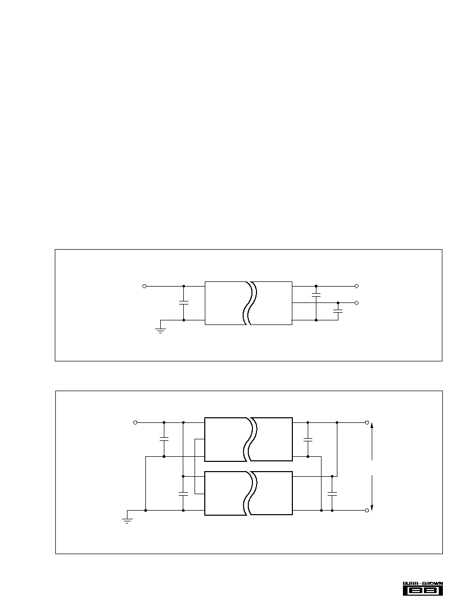
Connecting the DCP02 in Parallel
If the output power from one DCP02 is not sufficient, it is
possible to parallel the outputs of multiple DCP02s, as
shown in Figure 3. Again, the SYNC feature allows easy
synchronization to prevent power-rail beat frequencies at no
additional filtering cost.
DCP
02
+V
OUT
V
SUPPLY
+V
OUT
V
OUT
V
OUT
0V
V
S
0V
COM
FIGURE 3. Connecting Multiple DCP02s in Parallel.
DCP
02
0V
0V
V
OUT
V
SUPPLY
V
S
0V
DCP
02
V
OUT
2 x Power Out
SYNC
SYNC
V
S
0V
COM