Æ
Miniature, 1W Isolated
REGULATED DC/DC CONVERTERS
©
2000 Burr-Brown Corporation
PDS-1587A
Printed in U.S.A. May, 2000
DCR01
Series
International Airport Industrial Park ∑ Mailing Address: PO Box 11400, Tucson, AZ 85734 ∑ Street Address: 6730 S. Tucson Blvd., Tucson, AZ 85706 ∑ Tel: (520) 746-1111
Twx: 910-952-1111 ∑ Internet: http://www.burr-brown.com/ ∑ Cable: BBRCORP ∑ Telex: 066-6491 ∑ FAX: (520) 889-1510 ∑ Immediate Product Info: (800) 548-6132
For most current data sheet and other
product information, visit www.burr-brown.com
FEATURES
q
UL1950 RECOGNIZED
q
PDIP-18, SO-28
(1)
q
53W/in
3
(3.3W/cm
3
) POWER DENSITY
q
DEVICE-TO-DEVICE SYNCHRONIZATION
q
THERMAL PROTECTION
q
1000Vrms ISOLATION
q
400kHz SWITCHING
q
125 FITS AT 55
∞
C
q
±
10% INPUT RANGE
q
SHORT-CIRCUIT PROTECTED
q
5V, 12V, 24V INPUTS
q
3.3V, 5V OUTPUTS
q
HIGH EFFICIENCY
DESCRIPTION
DCR01 family is a series of high-efficiency, input-
isolated, output-regulated DC/DC converters. In addi-
tion to 1W nominal, galvanically-isolated output power
capability, this range of DC/DCs offer very low out-
put noise, thermal protection and high accuracy.
The DCR01 family is implemented in standard molded
IC packaging, giving standard JEDEC outlines suit-
able for high-volume assembly.
The DCR01 is manufactured using the same technol-
ogy as standard IC packages, thereby achieving very
high reliability.
NOTE: (1) SO version available Q3 2000.
APPLICATIONS
q
POINT-OF-USE POWER CONVERSION
q
DIGITAL INTERFACE POWER
q
GROUND LOOP ELIMINATION
q
POWER-SUPPLY NOISE REDUCTION
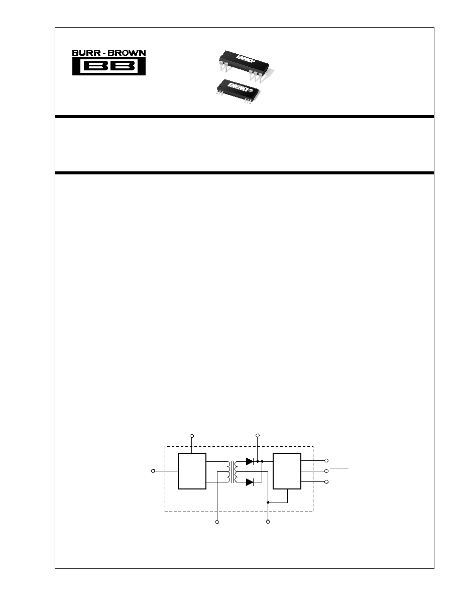
Input
Controller
LDO
Regulator
ENABLE
V
REC
SYNC
V
S
ERROR
V
OUT
0V
0V
DCR01
DCR01

2
DCR01
Æ
SPECIFICATIONS
At T
A
= +25
∞
C, V
S
= nominal, I
O
= 10mA, C
O
= 0.1
µ
F, unless otherwise specified.
DCR01 SERIES
PARAMETER
CONDITIONS
MIN
TYP
MAX
UNITS
OUTPUT
Setpoint
DCR010503
3.3
V
DCR010505
5
V
DCR011203
(2)
3.3
V
DCR011205
(2)
5
V
DCR012403
(3)
3.3
V
DCR012405
(3)
5
V
Setpoint Accuracy
0.5
2.0
%
Maximum Output Current
DCR010503
300
mA
DCR010505
200
mA
DCR011203
(2)
390
mA
DCR011205
(2)
200
mA
DCR012403
(3)
390
mA
DCR012405
(3)
200
mA
Output Short-Circuit Protected
Duration
Infinite
Line Regulation
DCR010503
1
mV/V
DCR010505
1
mV/V
DCR011203
(2)
1
mV/V
DCR011205
(2)
1
mV/V
DCR012403
(3)
1
mV/V
DCR012405
(3)
1
mV/V
Over Line and Load
DCR010503
10mA to 300mA Load, 4.5V to 5.5V Line
1.0
2.5
%
DCR010505
10mA to 200mA Load, 4.5V to 5.5V Line
1.0
2.5
%
DCR011203
10mA to 390mA Load, 10.8V to 13.2V Line
1.0
2.5
%
DCR011205
10mA to 200mA Load, 10.8V to 13.2V Line
1.0
2.5
%
DCR012403
10mA to 390mA Load, 21.6V to 26.4V Line
1.0
2.5
%
DCR012405
10mA to 200mA Load, 21.6V to 26.4V Line
1.0
2.5
%
Versus Temperature
≠40
∞
C to +85
∞
C
1.0
%
Ripple and Noise
DCR0105 Ripple
20MHz Bandwidth, 50% Load
5
mVp-p
C
IN
= 2.2
µ
F, C
FILTER
= 1
µ
F, C
OUT
= 0.1
µ
F
DCR0105 Noise
100MHz Bandwidth, 50% Load
35
mVp-p
C
IN
= 2.2
µ
, C
FILTER
= 1
µ
F, C
OUT
= 0.1
µ
F
INPUT
Nominal Voltage (V
S
)
DCR0105xx
5
V
DCR0112xx
12
V
DCR0124xx
24
V
Voltage Range
≠10
+10
%
Supply Current
DCR010503
I
O
= 0mA
18
mA
I
O
= 10mA
28
mA
I
O
= 300mA
335
mA
DCR010505
I
O
= 0mA
25
mA
I
O
= 10mA
40
mA
I
O
= 200mA
310
mA
DCR011203
(2)
I
O
= 0mA
13
mA
I
O
= 10mA
17
mA
I
O
= 390mA
173
mA
DCR011205
(2)
I
O
= 0mA
13
mA
I
O
= 10mA
18
mA
I
O
= 200mA
125
mA
DCR012403
(3)
I
O
= 0mA
15
mA
I
O
= 10mA
17
mA
I
O
= 390mA
94
mA
DCR012405
(3)
I
O
= 0mA
15
mA
I
O
= 10mA
17
mA
I
O
= 200mA
71
mA
Reflected Ripple Current
DCR010503, DCR01505
MHz Bandwidth, 100% Load
8
mAp-p
C
IN
= 2.2
µ
F, C
FILTER
= 1
µ
F
3
Æ
DCR01
ISOLATION
Voltage
1s Flash Test
1
kVrms
60s Test, UL1950
(1)
1
kVrms
Input/Output Capacitance
25
pF
OUTPUT ENABLE CONTROL
Logic High Input Voltage
2.0
V
REC
V
Logic High Input Current
2.0 < V
ENABLE
< V
REC
100
nA
Logic Low Input Voltage
≠0.2
0.5
V
Logic Low Input Current
0 < V
ENABLE
< 0.5
100
nA
DCR010503
V
DCR010505
V
ERROR FLAG
Logic High Open Collector Leakage
V
ERROR
= 5V
10
µ
A
Logic Low Output Voltage
Sinking 2mA
0.4
V
THERMAL SHUTDOWN
Junction Temperature
Temperature Activated
150
∞
C
Temperature Deactivated
130
∞
C
SYNCHRONIZATION PIN
Max External Capacitance on SYNC Pin
3
pF
Internal Oscillator Frequency
720
800
880
kHz
External Synchronization Frequency
720
880
kHz
External Synchronization Signal High
2.5
2.5
5.0
V
External Synchronization Signal Low
0
0.4
V
TEMPERATURE RANGE
Operating
≠40
+85
∞
C
NOTES: (1) During UL approval only. (2) DCR011203, DCR011205 available Q2 2000. (3) DCR0112403, DCR012405 available Q3 2000.
The information provided herein is believed to be reliable; however, BURR-BROWN assumes no responsibility for inaccuracies or omissions. BURR-BROWN assumes
no responsibility for the use of this information, and all use of such information shall be entirely at the user's own risk. Prices and specifications are subject to change
without notice. No patent rights or licenses to any of the circuits described herein are implied or granted to any third party. BURR-BROWN does not authorize or warrant
any BURR-BROWN product for use in life support devices and/or systems.
SPECIFICATIONS
(Cont.)
At T
A
= +25
∞
C, V
S
= nominal, I
O
= 10mA, C
O
= 0.1
µ
F, unless otherwise specified.
DCR01 SERIES
PARAMETER
CONDITIONS
MIN
TYP
MAX
UNITS
ELECTROSTATIC
DISCHARGE SENSITIVITY
This integrated circuit can be damaged by ESD. Burr-Brown
recommends that all integrated circuits be handled with
appropriate precautions. Failure to observe proper handling
and installation procedures can cause damage.
ESD damage can range from subtle performance degrada-
tion to complete device failure. Precision integrated circuits
may be more susceptible to damage because very small
parametric changes could cause the device not to meet its
published specifications.
Input Voltage:
DCR0105 ............................................................................................ 7V
DCR0112 .......................................................................................... 15V
DCR0124 .......................................................................................... 29V
Storage Temperature ...................................................... ≠60
∞
C to +125
∞
C
Lead Temperature (soldering, 10s) ................................................. 270
∞
C
ABSOLUTE MAXIMUM RATINGS
DCR01
Basic Model Number: 1W Product
Voltage Input:
5V In
Voltage Output:
5V Out
Package Code:
P = 18-Pin Plastic DIP, U = 28-Pin SO
(1)
NOTE: (1) SO version available Q3 2000.
ORDERING INFORMATION
05
05
( P )

4
DCR01
Æ
SO
PIN #
PIN NAME
DESCRIPTION
1
V
S
Voltage Input
2
V
S
Voltage Input
3
NC
No Connection
12
V
REC
Rectified Output
13
V
OUT
Output Ground
14
V
O
Voltage Output
15
DNC
Do Not Connect
16
ENABLE
Output Voltage Enable
17
ERROR
Error Flag Active Low
26
0V
IN
Input Ground
27
0V
IN
Input Ground
28
SYNC
Synchronization Input
PIN DEFINITION (PDIP)
PIN #
PIN NAME
DESCRIPTION
1
V
S
Voltage Input
2
NC
No Connection
7
V
REC
Rectified Output
8
0V
OUT
Output Ground
9
V
O
Voltage Output
10
DNC
Do Not Connect
11
ENABLE
Output Voltage Enable
12
ERROR
Error Flag Active Low
17
0V
IN
Input Ground
18
SYNC
Synchronization Input
NOTE: (1) SO version available Q3 2000.
Top View
PDIP
PIN CONFIGURATIONS
DCR01
1
2
7
8
9
18
17
12
11
10
V
S
NC
V
REC
0V
OUT
V
O
SYNC
0V
IN
ERROR
ENABLE
DNC
PIN DEFINITION (SO)
DCR01U
1
2
3
12
13
14
28
27
26
17
16
15
V
S
V
S
NC
V
REC
0V
OUT
V
O
SYNC
0V
IN
0V
IN
ERROR
ENABLE
DNC
PACKAGE
SPECIFIED
DRAWING
TEMPERATURE
PACKAGE
ORDERING
TRANSPORT
PRODUCT
PACKAGE
NUMBER
RANGE
MARKING
NUMBER
(1)
MEDIA
DCR010503P
PDIP-18
218-1
≠40
∞
C to +85
∞
C
DCR010503P
DCR010503P
Rails
DCR010505P
PDIP-18
218-1
≠40
∞
C to +85
∞
C
DCR010505P
DCR010505P
Rails
DCR010503U
(3)
SO-28
217-2
≠40
∞
C to +85
∞
C
DCR010503U
DCR010503U/1K
Tape and Reel
DCR010505U
(3)
SO-28
217-2
≠40
∞
C to +85
∞
C
DCR010505U
DCR010505U/1K
Tape and Reel
DCR011203P
(2)
PDIP-18
218-1
≠40
∞
C to +85
∞
C
DCR011203P
DCR011203P
Rails
DCR011203U
(1, 3)
SO-28
217-2
≠40
∞
C to +85
∞
C
DCR011203U
DCR011203U/1K
Tape and Reel
DCR011205P
(2)
PDIP-18
218-1
≠40
∞
C to +85
∞
C
DCR011205P
DCR011205P
Rails
DCR011205U
(1, 3)
SO-28
217-2
≠40
∞
C to +85
∞
C
DCR011205U
DCR011205U/1K
Tape and Reel
DCR012403P
(3)
PDIP-18
218-1
≠40
∞
C to +85
∞
C
DCR012403P
DCR012403P
Rails
DCR012403U
(1, 3)
SO-28
217-2
≠40
∞
C to +85
∞
C
DCR012403U
DCR012403U/1K
Tape and Reel
DCR012405P
(3)
PDIP-18
218-1
≠40
∞
C to +85
∞
C
DCR012405P
DCR012405P
Rails
DCR012405U
(1, 3)
SO-28
217-2
≠40
∞
C to +85
∞
C
DCR012405U
DCR012405U/1K
Tape and Reel
NOTE: (1) Models with a slash (/) are available only in Tape and Reel in the quantities indicated (e.g., /1K indicates 1000 devices per reel). Ordering 1000 pieces
of "DCR010503U/1K" will get a single 1000-piece Tape and Reel. (2) Available Q2 2000. (3) Available Q3 2000.
PACKAGE/ORDERING INFORMATION
5
Æ
DCR01
TYPICAL PERFORMANCE CURVES
At T
A
= +25
∞
C, V
S
= 5V, I
O
= 10mA, C
O
= 0.1
µ
F, unless otherwise specified.
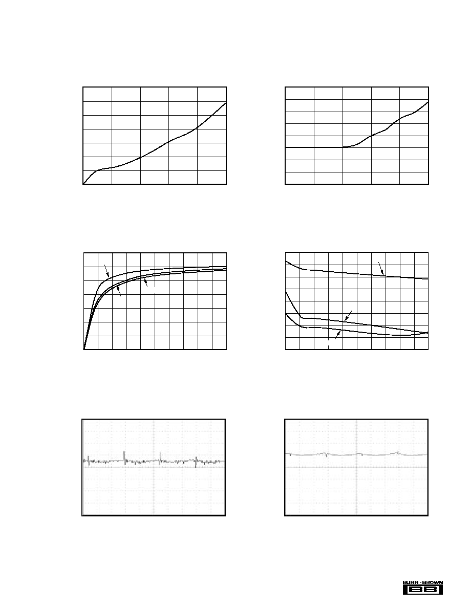
DCR0105 SERIES INPUT CURRENT
REFLECTED NOISE (100MHz Bandwidth)
500ns/div
40mA/div
DCR0105 SERIES INPUT
CURRENT REFLECTED RIPPLE
500ns/div
20mA/div
DCR0105 OUTPUT VOLTAGE RIPPLE
Load (%)
Ripple V
oltage (mVp-p)
14
12
10
8
6
4
2
0
20
40
60
80
100
0
DCR0105 OUTPUT NOISE (100MHz Bandwidth)
Load (%)
Noise (mVp-p)
80
70
60
50
40
30
20
10
0
20
40
60
80
100
0
DCR010503P EFFICIENCY
(V
IN
= 5V)
Load (%)
Ef
ficiency (%)
70
60
50
40
30
20
10
0
100
0
10
20
85
∞
C
25
∞
C
30
40
50
60
70
80
90
≠40
∞
C
DCR010503P V
OUT
vs LOAD
(V
IN
= 5V)
Load (%)
V
OUT
(V)
3.305
3.3
3.295
3.29
3.285
3.28
3.275
3.27
3.265
100
0
10
20
30
40
50
60
70
80
90
85
∞
C
25
∞
C
≠40
∞
C
6
DCR01
Æ
TYPICAL PERFORMANCE CURVES
(Cont.)
At T
A
= +25
∞
C, V
S
= 5V, I
O
= 10mA, C
O
= 0.1
µ
F, unless otherwise specified.
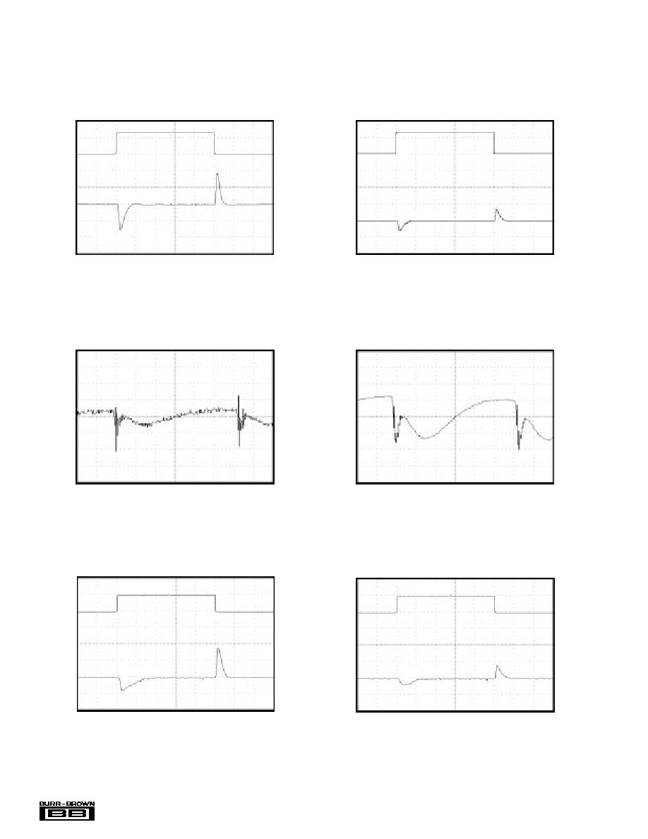
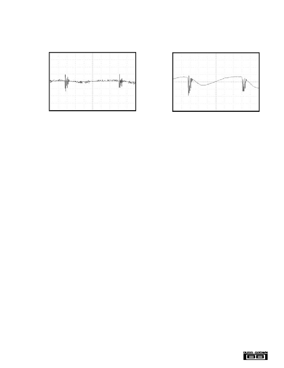
DCR010503P OUTPUT VOLTAGE NOISE
AT 100% LOAD (100MHz Bandwidth)
200ns/div
20mV/div
Load Current
Output Voltage
DCR010503P OUTPUT VOLTAGE RIPPLE
AT 100% LOAD (20MHz Bandwidth)
200ns/div
5mV/div
DCR010503P LOAD TRANSIENT RESPONSE
10
µ
s/div
30mA
Changing
to 325mA
200mV/div
Load Current
Output Voltage
DCR010503P LOAD TRANSIENT RESPONSE
10
µ
s/div
150mA
Changing
to 300mA
200mV/div
Load Current
Output Voltage
DCR010505P LOAD TRANSIENT RESPONSE
10
µ
s/div
20mA
Changing
to 200mA
200mV/div
Load Current
Output Voltage
DCR010505P LOAD TRANSIENT RESPONSE
10
µ
s/div
100mA
Changing
to 200mA
200mV/div
Load Current
Output Voltage
7
Æ
DCR01
TYPICAL PERFORMANCE CURVES
(Cont.)
At T
A
= +25
∞
C, V
S
= 5V, I
O
= 10mA, C
O
= 0.1
µ
F, unless otherwise specified.
DCR010505P OUTPUT VOLTAGE NOISE
AT 100% LOAD (100MHz Bandwidth)
200ns/div
20mV/div
DCR010505P OUTPUT VOLTAGE RIPPLE
AT 100% LOAD (20MHz Bandwidth)
200ns/div
5mV/div
FUNCTIONAL DESCRIPTION
OVERVIEW
The DCR01 series offers isolation from an unregulated
power supply operating from a choice of input voltages. The
DCR01's provide a variety of regulated output voltages at a
nominal output power of 1W or above.
POWER STAGE
The input supply is chopped at a frequency of 400kHz
(internal oscillator divided by 2), which is used to drive the
center-tapped toroidal transformer.
RECTIFICATION
The transformer's output is full wave rectified and smoothed
by the external capacitor connected to V
REC
.
REGULATOR
The internal low drop-out regulator provides a well-regu-
lated output voltage, throughout the operating range of the
device.
OSCILLATOR AND WATCHDOG
The DCR01 uses an internal saw-tooth generator to provide
the 800kHz on-board oscillator that is used to drive the
power switching circuit. The operation of the oscillator is
monitored by the watchdog, which will tri-state the output
driver circuit if the oscillator fails, or if the SYNC pin is
taken low, (shutdown mode). When the SYNC pin is re-
turned high, normal operation resumes.
SYNCHRONIZATION
If more than one DCR01 is being used, beat frequencies and
other electrical interference can be generated. This is due to
the small variations in switching frequencies between the
converters.
The DCR01 overcomes this by allowing devices to be
synchronized to one another. Up to eight devices can be
synchronized by connecting the SYNC pins together, with
care being taken to minimize the capacitance of tracking.
Significant stray capacitance on the SYNC pin will have the
effect of reducing the frequency of the internal oscillator. If
this is large, the DCR01 may be taken out with its optimized
operating parameters and saturation of the magnetics may
result, damaging the device.
If devices are synchronized, it should be noted that all
devices will draw maximum current simultaneously at start
up. This can cause the input voltage to dip. Should it fall
below the minimum input voltage, the devices may not start
up. A 2.2
µ
F capacitor (low ESR) should be connected as
close to the device input pins as possible for the 5V input
devices and a 0.47
µ
F capacitor for the 12V and 24V devices.
If more than eight devices are required to be synchronized,
it is recommended that external synchronization be used.
Details are contained in Burr-Brown's Application Bulletin
AB-153.
CONSTRUCTION
The DCR01 is manufactured using the same technology as
standard IC packages. There is no substrate within the
package. The DCR01 is constructed using a driver IC, Low
Dropout Voltage Regulator, rectifier diodes and a wound
magnetic toroid, all mounted on a leadframe. The DCR01
requires no special PCB assembly processing, as there is no
solder within the package. The result is an isolated DC/DC
converter with inherently high reliability.
ADDITIONAL FUNCTIONS
DISABLE/ENABLE
The DCR01 can be disabled or enabled by driving the SYNC
pin using an open drain CMOS gate. If the SYNC pin is

8
DCR01
Æ
pulled low, the DCR01 will be disabled. The disable time
depends upon the external loading. The internal disable
function is implemented in 2
µ
s. Removal of the pull down
will enable the DCR01.
Capacitance loading on the SYNC pin should be minimized
in order to prevent a reduction in the internal oscillator`s
frequency. See Application Bulletin AB-153 External Syn-
chronization of the DCP01/02 Series of DC/DC Converters.
This document contains information on how to null the
effects of additional capacitance on the sync pin. The oscil-
lators frequency can be measured at V
REC
, as this is the
fundamental frequency of the ripple component.
OUTPUT ENABLE/DISABLE
The regulated output of the DCR01 can be disabled by
pulling the ENABLE pin low. Holding the ENABLE pin
high enables the regulated output voltage, thus allowing the
output to be controlled from the isolated side.
ERROR FLAG
The DCR01 has an Error pin which provides a `power good'
flag, as long as the internal regulator is in regulation.
DECOUPLING
Ripple Reduction
Due to the very low forward resistance of the DMOS
switching transistors, high current demands are placed upon
the input supply for a short time. By using a good quality
low Equivalent Series Resistance (ESR) capacitor of 2.2
µ
F
(minimum) for the 5V input devices and a 0.47
µ
F capacitor
for the 12V and 24V devices, placed close to the IC supply
input pins, the effects on the power supply can be mini-
mized.
The high switching frequency of 400kHz allows relatively
small values of capacitors to be used for filtering the recti-
fied output voltage. A good quality low ESR capacitor of
1
µ
F placed close to the V
REC
pin and output ground will
reduce the ripple.
It is not recommended that the DCR01 be fitted using an
IC socket as this will degrade performance.
The output at V
REC
is full wave rectified and produces a
ripple of 800kHz.
It is recommended that a 0.1
µ
F low ESR capacitor is
connected close to the output pin and ground to reduce noise
on the output. The capacitor values listed are minimum
values. If lower ripple is required then the filter capacitor
should be increased in value to 0.47
µ
F.
NOTE: As with all switching power supplies the best
performance is only obtained with low ESR capacitors
connected close to the switcher. If low ESR capacitors are
not used, the ESR will generate a voltage drop when the
capacitor is supplying the load power. Often a larger capaci-
tor is chosen for this purpose when a low ESR smaller
capacitance would perform as well.
PCB LAYOUT
RIPPLE AND NOISE
Careful consideration should be given to the layout of the
PCB in order for the best results to be obtained.
The DCR01 is a switching power supply and as such can
place high peak current demands on the input supply. In
order to avoid the supply falling momentarily during the fast
switching pulses, ground and power planes should be used
to track the power to the input of DCR01, this will also serve
to reduce noise on the circuit. If this is not possible, the
supplies must be connected in a star formation, with the
tracks made as wide as possible.
If the SYNC pin is being used, the tracking between device
SYNC pins should be short to avoid stray capacitance. If the
SYNC pin is not being used it is advisable to place a guard
ring (connected to input ground) around this pin to avoid any
noise pick up.
The output should be taken from the device using ground
and power planes. This will ensure minimum losses.
A good quality low ESR capacitor placed as close as
practicable across the input will reduce reflected ripple and
ensure a smooth start up.
A good quality low ESR capacitor placed as close as
practicable across the rectifier output terminal and output
ground will give the best ripple and noise performance.
THERMAL MANAGEMENT
Due to the high power density of this device, it is advisable
to provide a ground plane on the output. The output regula-
tor is mounted on a copper leadframe, and a ground plane
will serve as an efficient heatsink.
9
Æ
DCR01
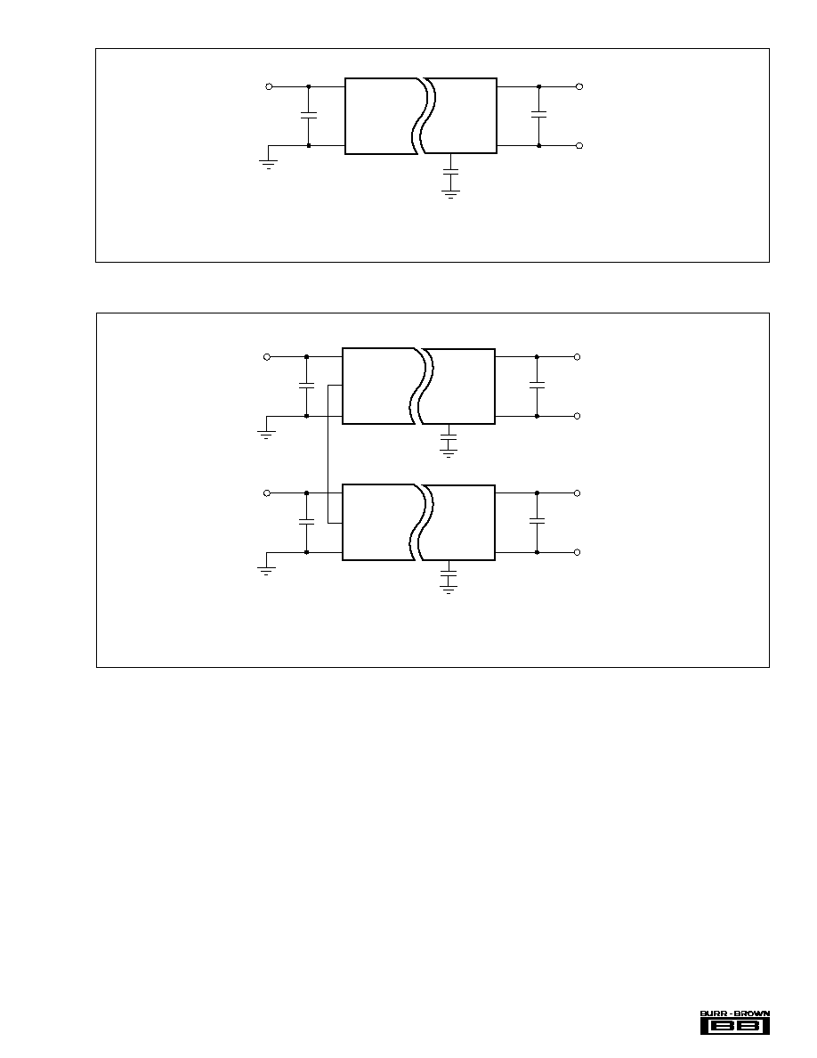
FIGURE 1. DCR01 with a Single Output.
FIGURE 2. Self-Synchronizing DCR01s with a Dual Output.
DCR
01
V
OUT
V
REC
V
IN
C
IN
(1)
C
OUT
= 0.1
µ
F
C
FILTER
= 1
µ
F
V
O1
0 V
OUT
0V
V
S
0V
NOTE: (1) 2.2
µ
F capacitor with low ESR for 5V
devices and 0.47
µ
F for 12V and 24V devices.
DCR
01
V
OUT
V
REC
V
IN
V
O1
0 V
OUT
0V
V
S
SYNC
0V
DCR
01
V
OUT
V
REC
V
IN
V
O2
0 V
OUT
0 V
OUT
0 V
OUT
0V
V
S
SYNC
0V
NOTE: (1) 2.2
µ
F capacitor with low ESR for 5V
devices and 0.47
µ
F for 12V and 24V devices.
C
IN
(1)
C
OUT
= 0.1
µ
F
C
IN
(1)
C
OUT
= 0.1
µ
F
C
FILTER
= 1
µ
F
C
FILTER
= 1
µ
F