 | –≠–ª–µ–∫—Ç—Ä–æ–Ω–Ω—ã–π –∫–æ–º–ø–æ–Ω–µ–Ω—Ç: DDC101 | –°–∫–∞—á–∞—Ç—å:  PDF PDF  ZIP ZIP |

20-BIT ANALOG-TO-DIGITAL CONVERTER
DDC101
DESCRIPTION
The DDC101 is a precision, wide dynamic range, charge
digitizing A/D converter with 20-bit resolution. Low
level current output devices, such as photosensors, can be
directly connected to its input. The most stringent accu-
racy requirements of many unipolar output sensor appli-
cations occur at low signal levels. To meet this require-
ment, Burr-Brown developed the adaptive delta modula-
tion architecture of the DDC101 to provide linearly
improving noise and linearity errors as the input signal
level decreases. The DDC101 combines the functions of
current-to-voltage conversion, integration, input program-
mable gain amplification, A/D conversion, and digital
filtering to produce precision, wide dynamic range re-
sults. The input signal can be a low level current con-
nected directly into the unit or a voltage connected
through a user selected resistor. Although the DDC101 is
optimized for unipolar signals, it can also accurately
digitize bipolar input signals. The patented delta modula-
tion topology combines charge integration and digitiza-
tion functions. Oversampling and digital filtering reduce
system noise dramatically. Correlated Double Sampling
(CDS) captures and eliminates steady state and conver-
sion cycle dependent offset and switching errors that are
not eliminated with conventional analog circuits.
The DDC101 block diagram is shown below. During
conversion, the input signal is collected on the internal
integration capacitance for a user determined integration
period. A high precision, autozeroed comparator samples
the analog input node. Tracking logic updates the internal
high resolution D/A converter at a 2MHz rate to maintain
the analog input at virtual ground. A user programmable
digital filter oversamples the tracking logic's output. The
digital filter passes a low noise, high resolution digital
output to the serial I/O register. The serial outputs of
multiple DDC101 units can be easily connected together
in series or parallel if desired to minimize interconnections.
q
MONOLITHIC CHARGE INPUT ADC
q
DIGITAL FILTER NOISE REDUCTION:
0.9ppm, rms
q
DIGITAL ERROR CORRECTION: CDS
q
CONVERSION RATE: Up to 15kHz
q
USER FRIENDLY EVALUATION FIXTURE
APPLICATIONS
FEATURES
q
DIRECT PHOTOSENSOR DIGITIZATION
q
PRECISION INSTRUMENTATION
q
INFRARED PYROMETRY
q
PRECISION PROCESS CONTROL
q
CT SCANNER DAS
q
CHEMICAL ANALYZERS
C
INT
Digital Integration,
Tracking and
Control Logic
Digital Filter and
Error Correction
Serial I/O
Register
Serial In
Serial Out
Reset
DAC
CDAC
DDC101 Integrated Circuit
Comparator
V
REF
Analog
Input
Ground
Setup
Oversampled
Digital Out
18 Bits
20 Bits
Test In
+V
S
Test Current
©
1993 Burr-Brown Corporation
PDS-1211E
Printed in U.S.A. March, 1998
Æ
International Airport Industrial Park ∑ Mailing Address: PO Box 11400, Tucson, AZ 85734 ∑ Street Address: 6730 S. Tucson Blvd., Tucson, AZ 85706 ∑ Tel: (520) 746-1111 ∑ Twx: 910-952-1111
Internet: http://www.burr-brown.com/ ∑ FAXLine: (800) 548-6133 (US/Canada Only) ∑ Cable: BBRCORP ∑ Telex: 066-6491 ∑ FAX: (520) 889-1510 ∑ Immediate Product Info: (800) 548-6132
DDC101
Æ
DDC101
2
TABLE OF CONTENTS
Section 1 ............. Basic Theory of Operation
2 ............. Specifications
3 ............. Pin Descriptions
4 ............. Timing Diagrams
5 ............. Discussion of Specifications
6 ............. Detailed Theory of Operation
7 ............. Applications Information
8 ............. Mechanical
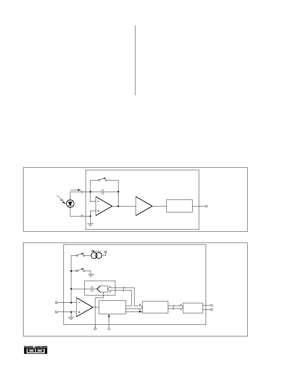
The second block diagram, Figure 2, shows the DDC101
circuit architecture which implements these functions
monolithically. During each conversion, the input signal
current is collected on the internal integration capacitance,
C
INT
, as charge for a user determined integration period, T
INT
.
As the integration capacitor collects input charge, the track-
ing logic updates the internal high resolution D/A converter
at a 2MHz rate to maintain the analog input node at virtual
ground.
The digital filter oversamples the tracking logic's output at
the beginning and end of each integration period to produce
two oversampled data points. The DDC101 measures the
charge accumulated in the integration and performs corre-
lated double sampling (CDS) by subtracting these two data
points. CDS eliminates integration cycle dependent errors
such as charge injection, offset voltage, and reset noise since
these errors are measured with the signal at each of the two
data points. The number of oversamples, and thus the fre-
quency response of the digital filter, is user programmable.
The digital filter passes a low noise, high resolution digital
output to the serial I/O register. Since the timing control of
the serial I/O register is independent of the DDC101 conver-
sion process, the outputs of multiple DDC101 units can be
connected together in series or parallel to minimize intercon-
nections.
SECTION 1
BASIC THEORY OF OPERATION
The basic function of the DDC101 is illustrated in the
Simplified Equivalent Circuit shown in Figure 1. The opera-
tion is equivalent to the functions performed by a very high
quality, low bias current switched integrator followed by a
precision floating point programmable gain amplifier and
ending with a high resolution A/D converter.
FIGURE 1. Simplified Equivalent Circuit of DDC101 to Illustrate Function.
FIGURE 2. DDC101 Block Diagram.
C
INT
Digital Integration,
Tracking and
Control Logic
Digital Filter and
Error Correction
Serial I/O
Register
Serial In
Serial Out
Reset
DAC
CDAC
DDC101 Integrated Circuit
Comparator
V
REF
Analog
Input
Ground
Setup
Oversampled
Digital Out
18 Bits
20 Bits
Test In
+V
S
Test Current
C
INT
Data Out
Reset
Switched Integrator
Programmable Gain
Amplifier
A/D Converter
and Control Logic
Sensor
i Signal
3
DDC101
Æ
The information provided herein is believed to be reliable; however, BURR-BROWN assumes no responsibility for inaccuracies or omissions. BURR-BROWN
assumes no responsibility for the use of this information, and all use of such information shall be entirely at the user's own risk. Prices and specifications are subject
to change without notice. No patent rights or licenses to any of the circuits described herein are implied or granted to any third party. BURR-BROWN does not
authorize or warrant any BURR-BROWN product for use in life support devices and/or systems.
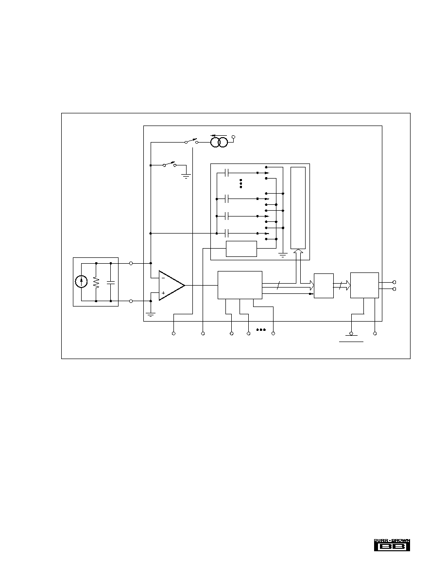
An internal test current source is provided for basic func-
tionality testing and diagnostics. This approximately 100nA
current source is pin activated and sums with the external
input current.
Figure 3 shows a more detailed circuit configuration of the
DDC101. The single integration capacitor, C
INT
, and the
D/A converter have been replaced with a high resolution
Capacitor Digital-to-Analog Converter (CDAC). By switch-
ing between ground and V
REF
the binary weighted capacitor
array of the CDAC accumulates the input signal's charge to
keep the comparator input at virtual ground.
FIGURE 3. DDC101 Detailed Circuit Diagram.
Reset
Comparator
Sensor
Serial I/O
Register
DATA
INPUT
DATA
OUTPUT
High
Resolution
Digital Out
3rd Order Digital
Integration,
Tracking and
Control Logic
Digital
Filter
Oversampled
Digital Out
C
INT
Buffer
V
REF
SYSTEM
CLOCK
System Control
DATA
CLOCK
DATA
TRANSMIT
CDAC
DDC101
+V
S
Test Current
TEST
In
ANALOG
In
ANALOG
COMMON
18 Bits
20 Bits

Æ
DDC101
4
SECTION 2
SPECIFICATIONS
ELECTRICAL
All specifications with unipolar current input range, T
INT
= 1ms, correlated double sampling enabled, System Clock = 2MHz, V
REF
= ≠2.5V, T
A
= +25
∞
C and V
S
=
±
5VDC,
unless otherwise noted.
DDC101
PARAMETER
CONDITIONS
MIN
TYP
MAX
UNITS
INPUTS
Charge Input
(6)
Unipolar Input Range
BTC Output Code
≠1.95
500
pC/Integration
Bipolar Input Range
BTC Output Code
≠251.95
250
pC/Integration
Input Current
Unipolar or Bipolar Range
7.8
µ
A
Current Input Range Examples
(10)
Unipolar Input Range
T
INT
= 100
µ
s
≠0.0195
5
µ
A
Unipolar Input Range
T
INT
= 1ms
≠1.95
500
nA
Bipolar Input Range
T
INT
= 100
µ
s
≠2.5195
2.5
µ
A
Bipolar Input Range
T
INT
= 1ms
≠251.95
250
nA
Voltage Input Examples
(10)
Unipolar Input Range
(2)
R
IN
= 10M
, T
INT
= 1ms
≠0.0195
5
V
Bipolar Input Range
(2)
R
IN
= 10M
, T
INT
= 1ms
≠2.5195
2.5
V
DYNAMIC CHARACTERISTICS
Conversion Time
64
256 x 10
6
µ
s
Integration Time
64
10
6
µ
s
System Clock Input
0.5
2
MHz
ACCURACY
Unipolar Mode Noise
Noise, Low Level Current Input
(1)
C
SENSOR
= 0pF, L = 8
0.9
ppm of FSR, rms
(3)
Noise, Low Level Current Input
(1)
C
SENSOR
= 0pF, L = 1
1.6
ppm of FSR, rms
Noise, Low Level Current Input
(1)
C
SENSOR
= 100pF, L = 1
2.1
3
ppm of FSR, rms
Noise, Low Level Current Input
(1)
C
SENSOR
= 500pF, L = 1
4.2
ppm of FSR, rms
Noise, Voltage Input
(1, 2)
R
IN
20M
1.9
ppm of FSR, rms
Differential Linearity Error
Unipolar Input Range
Entire Range
±
0.005% Reading
±
0.5ppm FSR, max
0.1% FSR Input
±
0.00006
% of FSR
1% FSR Input
±
0.00010
% of FSR
10% FSR Input
±
0.00055
% of FSR
Unipolar or Bipolar Input Range
±
0.0015
% of FSR
Integral Linearity Error
Unipolar Input Range
(11)
0 to 500 pc/Integration
±
0.0244% Reading
±
2.5ppm FSR, max
≠1.95 to 0 pc/Integration
±
0.0244% Reading
±
3.0ppm FSR, max
0.1% FSR Input
±
0.00028
% of FSR
1% FSR Input
±
0.00050
% of FSR
10% FSR Input
±
0.0027
% of FSR
Unipolar or Bipolar Input Range
(11)
±
0.003
% of FSR
No Missing Codes
Unipolar Input Range
18
Bits
Bipolar Input Range
16
Bits
Input Bias Current
T
A
= +25
∞
C
3
10
pA
DC Gain Error
±
0.5
±
2
% of FSR
Output Offset Error
(8)
±
0.5
ppm of FSR
Input Offset Voltage
(8)
±
0.5
±
2
mV
External Voltage Reference, V
REF
≠2.5
VDC
Internal Test Signal
100
nA
Internal Test Signal Accuracy
±
20
nA
Gain Sensitivity to V
REF
V
REF
= 2.5V
±
0.1V
1:1
PSRR
80
90
dB
PERFORMANCE OVER TEMPERATURE
Output Offset Drift
(8)
not including bias current drift
0
µ
V/
∞
C
Input Offset Voltage Drift
(8)
1
µ
V/
∞
C
Input Bias Current Drift
+25
∞
C to +45
∞
C
0.1
0.5
pA/
∞
C
Input Bias Current
T
A
= +85
∞
C
8
40
pA
Gain Drift
(4)
±
15
ppm/
∞
C
DIGITAL INPUT/OUTPUT
Logic Family
TTL Compatible CMOS
Logic Level: V
IH
I
IH
= +5
µ
A
+2.0
+V
CC
V
V
IL
I
IL
= +5
µ
A
≠0.3
+0.8
V
V
OH
I
OH
= 2 TTL Loads
+2.4
+V
CC
V
V
OL
I
OL
= 2 TTL Loads
0.0
0.4
V
Data Clock
Data I/O
8
MHz
SETUP Code I/O
(9)
4
MHz
Data Format
Straight Binary
Unipolar or Bipolar Range
20
Bits
Two's Complement
Unipolar or Bipolar Range
21
Bits

5
DDC101
Æ
SPECIFICATIONS
(CONT)
ELECTRICAL
All specifications with unipolar current input range, T
INT
= 1ms, correlated double sampling enabled, System Clock = 2MHz, V
REF
= ≠2.5V, T
A
= +25
∞
C and V
S
=
±
5VDC,
unless otherwise noted.
DDC101
PARAMETER
CONDITIONS
MIN
TYP
MAX
UNITS
POWER SUPPLY REQUIREMENTS
Operation
(5)
±
4.75
±
5
±
5.25
VDC
Quiescent Current, Positive Supply
V
S
+ = +5VDC, V
DD
+ = +5VDC
15.6
19.5
mA
Analog, V
S
+
8.9
mA
Digital, V
DD
+
6.7
mA
Quiescent Current, Negative Supply
V
S
≠ = ≠5VDC
18.0
22.5
mA
Operating Power
170
mW
TEMPERATURE RANGE
Operating
≠40
+85
∞
C
Storage
≠60
+100
∞
C
NOTES: (1) Input = low level (less than 1% of Full Scale); Full Scale I
IN
= 500nA; T
INT
= 1ms; Unipolar Input Range; Acquisition Time = 16 clock cycles, Oversampling = 128. (2) Voltage input is converted through user
provided input resistor, R
IN
. (3) FSR is Full Scale Range. (4) Gain Drift does not include the drift of the external reference. (5) V
DD
+ must be less than or equal to V
S
+. See Section 7 for recommended connections. (6)
Straight Binary output code has slightly different Charge Range. See Section 6. (8) Input offset voltage is nulled by autozero circuitry and causes no output error. See Section 6 (Internal Error Correction). (9) This is
the maximum clock frequency at which SETUP codes can be written to and read from the DDC101. (10) For other input current and voltage configurations, see Discussion of Specifications and Detailed Theory of Operation
sections. (11) A best-fit straight line method is used to determine linearity. Two different best-fit straight lines are used for the two unipolar integral linearity specifications. Acquisition Time = 16 clock cycles, Oversampling
= 128.
Analog Inputs
Input Current ............................................................ 100mA, momentary
Input Current .............................................................. 10mA, continuous
Input Voltage ................................................... V
S
+ +0.5V to V
S
≠ ≠0.5V
Power Supply
V
S
+ .................................................................................................. + 7V
V
S
≠ .................................................................................................... ≠7V
V
DD
+ ................................................................................. must be
V
S
+
Maximum Junction Temperature ................................................... +165
∞
C
ABSOLUTE MAXIMUM RATINGS
PACKAGE/ORDERING INFORMATION
PACKAGE
THERMAL
DRAWING
RESISTANCE (
JA
)
PRODUCT
PACKAGE
NUMBER
(1)
(
∞
C/W)
DDC101U
24-Lead SOIC
239
100
NOTE: (1) For detailed drawing and dimension table, please see end of data
sheet, or Appendix C of Burr-Brown IC Data Book.
The information provided herein is believed to be reliable; however, BURR-BROWN assumes no responsibility for inaccuracies or omissions. BURR-BROWN assumes
no responsibility for the use of this information, and all use of such information shall be entirely at the user's own risk. Prices and specifications are subject to change
without notice. No patent rights or licenses to any of the circuits described herein are implied or granted to any third party. BURR-BROWN does not authorize or warrant
any BURR-BROWN product for use in life support devices and/or systems.
ELECTROSTATIC
DISCHARGE SENSITIVITY
This integrated circuit can be damaged by ESD. Burr-Brown
recommends that all integrated circuits be handled with ap-
propriate precautions. Failure to observe proper handling and
installation procedures can cause damage.
ESD damage can range from subtle performance degradation
to complete device failure. Precision integrated circuits may
be more susceptible to damage because very small parametric
changes could cause the device not to meet published
specifications.

Æ
DDC101
6
PIN CONFIGURATION
Top View
24-Lead SOIC
SECTION 3
PIN DESCRIPTIONS
1
2
3
4
5
6
7
8
9
10
11
12
24
23
22
21
20
19
18
17
16
15
14
13
REFERENCE BUFFER BYPASS
V
REF
TEST In
RESET SETUP In
SETUP
READ DATA/SETUP
DATA TRANSMIT In
OVERFLOW + Out
OVERFLOW ≠ Out
DATA VALID Out
DATA OUTPUT
DIGITAL GROUND
V
S
≠, ANALOG
ANALOG COMMON
ANALOG In
ANALOG COMMON
V
S
+, ANALOG
V
S
+, ANALOG
RESET SYSTEM In
FDS (Final Data Point Start) In
SYSTEM CLOCK
DATA CLOCK
DATA INPUT
V
DD
+, DIGITAL
PIN
NUMBER
NAME
DESCRIPTION
1
V
S
≠, ANALOG
Negative analog power supply voltage, ≠5VDC.
2
ANALOG COMMON
Analog ground point.
3
ANALOG INPUT
Input for low level current signal. Photosensor can be directly connected to this input. With a resistor in series,
DDC101 will convert a voltage input.
4
ANALOG COMMON
Analog ground point.
5
V
S
+, ANALOG
Positive analog power supply voltage, +5VDC. Hardwire to pin 6.
6
V
S
+, ANALOG
Positive analog power supply voltage, +5VDC. Hardwire to pin 5.
7
RESET SYSTEM In
This input resets DDC101, but does not reset the SETUP register. The DDC101 system is reset when this pin
is active; reset action is removed when the pin is inactive.
8
FDS In
This is Final Data point Start input. This input is the basic user control of the integration and conversion timing.
When it becomes active, the DDC101 starts collection of the M, final data point samples. The beginning of the
next integration time is exactly M system clock periods after the Final Data point Start command when operating
in the continuous mode.
9
SYSTEM CLOCK
This clock input sets the basic sampling rate of the DDC101. The DDC101 is specified with a clock speed of
2MHz. The clock speed can be 0.5MHz to 2.0MHz.
10
DATA CLOCK
This clock input controls the data transfer rate for the serial DATA INPUT and DATA OUTPUT ports. The DATA
CLOCK is independent of the SYSTEM CLOCK. This allows the DATA CLOCK to be operated at higher or lower
speeds than the SYSTEM CLOCK. For best noise performance, data should not be transmitted and the DATA
CLOCK should not be active during the initial and final data point collection. If data is being transmitted during
the initial and final data point collection periods, the DATA CLOCK should be synchronized to the SYSTEM
CLOCK, to minimize added noise. DATA CLOCK can be connected to SYSTEM CLOCK, so that the same clock
is used for both; however, for best noise performance, the DATA CLOCK input should be active only when data
is transmitted.
11
DATA INPUT
This input can be used to "daisy chain" the output of several DDC101s together to minimize wiring. The output
register of the DDC101 acts as a shift register to pass through the output of previously connected DDC101 units.
In this way, multiple DDC101 units can convert simultaneously then sequence the data out serially on the same
data line with one common control line and one common data line for all DDC101 units.
12
V
DD
+, DIGITAL
Digital power supply, +5VDC. V
DD
+ must be less than or equal to V
S
+.
13
DIGITAL GROUND
Digital ground point.
14
DATA OUTPUT
This output provides serial digital data clocked out at user controlled DATA CLOCK rate. Output data format
is a 21-bit Binary Two's Complement word or a 20-bit Straight Binary word. The data word is transmitted MSB
first. When DATA TRANSMIT is not active DATA OUTPUT tri-states.
15
DATA VALID
This output is activated when conversion is complete and remains active until the DATA TRANSMIT input is
activated.
16
OVERFLOW≠
The OVERFLOW output signals each provide an open collector output so that the overflow outputs from several
17
OVERFLOW+
DDC101s can easily be connected (wire ORed) together to a common pull-up resistor. They are activated when
the input is beyond the acceptable range during conversion. Specifically, they are activated when the internal
D/A converter input or digital filter exceeds full scale. They are Cleared at the end of conversion 1/2 clock cycle
after DATA VALID high. DATA VALID can be used to capture OVERFLOW data into an external register.
7
DDC101
Æ
PIN DESCRIPTIONS
(CONT)
PIN
NUMBER
NAME
DESCRIPTION
18
DATA TRANSMIT In
This input controls the transmission of data from the serial I/O register of the DDC101. It can be activated
anytime after DATA VALID out becomes active. It must remain active until all data has been collected from the
serial I/O register(s) of all DDC101s in the data path.
19
READ DATA/
This input can be used to read back the current SETUP data. When this input is held high, the output from DATA
SETUP In
OUTPUT is the data collected by the DDC101. When this input is pulled low, an internal shift register is loaded
with the current SETUP data on the rising edge of DATA CLOCK. This SETUP data shift register is logically
connected between DATA INPUT and DATA OUTPUT pins and can be read in the same way that the data
output is read. SETUP data read back does not invalidate data already stored in the DDC101's serial I/O register
or data being
collected by the DDC101, although digital noise concerns should be considered as
discussed in DATA CLOCK.
20
SETUP In
This input pin controls the DDC101 SETUP. A 12-bit digital word transmitted into this pin controls Acquisition
Time, K, Oversampling, M, Multiple Integrations, L, Input Range and Output Data Format. The DDC101 reads
the SETUP code at this pin after the RESET SETUP input transitions from active to inactive. The SETUP code
is read into the SETUP register on the 12 positive data clock transitions following that transition.
21
RESET SETUP
Resets SETUP register only, does not reset balance of DDC101. The DDC101 reads SETUP input data after
this input transitions from active (reset) to inactive.
22
TEST In
This is a digital input that controls the connection of an internal DC current source to the DDC101's input. TEST
In exercises the DDC101 and is intended to test for functionality only. The typical test input current is 100nA
±
20nA. The quiescent current of the DDC101 increases by approximately 1mA when TEST In is active. When
TEST is HIGH, the internal current source is ON and current is flowing into the DDC101 input. When TEST is
LOW, the current source is disconnected from the input.
23
V
REF
An external ≠2.5V reference must be connected to the REFERENCE In pin. Use of an external reference allows
multiple DDC101s to use the same system reference for optimum channel matching. The external reference
should be filtered to minimize noise contribution (see Figure 24).
24
REFERENCE
An external capacitor of 10
µ
F should be connected to this node to provide proper operation of the internal
BUFFER BYPASS
D/A converter. The REFERENCE In pin is connected to an internal reference buffer
amplifier. The internal reference buffer drives the internal CDAC. This buffer output is not intended for external
use.
SECTION 4
TIMING CHARACTERISTICS
All specifications with Unipolar input range, T
INT
= 1ms, Current Input, Correlated Double Sampling enabled, Sys Clock = 2MHz, V
REF
= ≠2.5V, T
A
= +25
∞
C and
V
S
=
±
5VDC, unless otherwise noted.
SYMBOL
DESCRIPTION
MIN
TYP
MAX
UNITS
t
1
FDS Setup
30
ns
t
2
FDS width, Continuous Conversion
50
(M≠1) Clocks+t
1
+100ns
ns
t
3
FDS width, Asynchronous Conversion
M Clocks+t
1
ns
t
4
FDS HIGH to start of next integration, Asynchronous Conversion
50
ns
t
5
Setup time for RESET SETUP HIGH to DATA CLOCK HIGH
60
ns
t
6
Setup time for Setup Codes data valid before rising edge of DATA Clock
30
ns
t
7
Hold time for Setup Codes data valid after rising edge of DATA Clock
30
ns
t
8
Propagation delay from rising edge of SYSTEM CLOCK to DATA VALID LOW
50
ns
t
9
Propagation delay from DATA TRANSMIT LOW to DATA VALID HIGH
35
ns
t
10
Setup time for DATA CLOCK LOW to DATA TRANSMIT LOW
30
ns
t
11
Propagation delay from DATA TRANSMIT LOW to valid data out
30
ns
t
12
Hold time that Data output is valid after falling edge of DATA CLOCK
10
ns
t
13
Propagation delay from DATA TRANSMIT HIGH to Data Output tri-stated
40
ns
t
14
Propagation delay from falling edge of SYSTEM CLOCK to OVERFLOW+ and
25
ns
OVERFLOW≠cleared
t
15
SYSTEM CLOCK pulse width HIGH
240
ns
t
16
SYSTEM CLOCK pulse width LOW
240
ns
t
17
DATA VALID LOW to DATA TRANSMIT LOW, Single DDC101
30
(LxN≠21) Clocks
ns

Æ
DDC101
8
FIGURE 6. DATA TRANSMIT Timing Diagram.
FIGURE 4. Conversion Timing Diagrams.
Input
Range
Output
Format
SETUP In
DATA CLOCK
(4MHz, max for setup)
ACQ
LSB
t
5
RESET SETUP In
ACQ
MSB
Read
Read
Read
Read
t
6
t
7
FIGURE 5. Input/Output Timing Diagram--SETUP Timing Diagram.
SYSTEM
CLOCK
DATA VALID
Out
DATA TRANSMIT
In
DATA OUTPUT
DATA CLOCK
(8MHz, max for data)
t
10
DDC(1)
Bit 1, MSB
DDC(n)
Bit 21, LSB
DDC
(n+1)
Bit 1
Output Disabled
Last DDC
Bit 21
Output Enabled
Output Disabled
t
12
Data can be read on rising or falling edge of Data Clock
DATA TRANSMIT In resets DATA VALID Out.
t
9
t
11
t
13
t
17
t
8
Continuous Integration Timing
Non-Continuous Integration Timing
SYSTEM
CLOCK
FDS In
Internal
Oversampling
Interval
Internal
Reset
SYSTEM
CLOCK
FDS In
Internal
Oversampling
Interval
Internal
Reset
FDS In should be coincident with negative clock.
FDS initiates oversampling period.
M Clock Periods
End of oversample period
initiates reset for next integration.
FDS In should be coincident with negative clock.
FDS initiates oversampling period.
End of FDS In
initiates end of Internal Reset.
End of oversample
period initiates
reset.
When Internal Reset period ends,
next integration begins.
DATA VALID
Out
t
2
t
1
t
3
DATA VALID Out
Next integration begins when 1 clock
period wide Internal Reset ends.
M Clock Periods
t
4
T
INT
'
T
INT

9
DDC101
Æ
TIMING DIAGRAMS (CONT)
FIGURE 7. OVERFLOW Out Monitoring Timing Diagram.
OVERFLOW ≠ Out
OVERFLOW + Out
t
8
DATA VALID Out
Read
Read
Clear
SYSTEM CLOCK In
t
14
DATA VALID Out can be used to latch data from the overflow status outputs.
Clear
FIGURE 8. System Clock Timing.
t
15
SYSTEM CLOCK In
SYSTEM CLOCK
t
16

Æ
DDC101
10
TYPICAL PERFORMANCE CURVES
ELECTRICAL
System Clock = 2MHz, V
S
=
±
5VDC, V
REF
= ≠2.5V, L = 1 Integration/Conversion, and T
A
= +25
∞
C, unless otherwise noted.
SINAD AT 10kHz CONVERSION, UNIPOLAR INPUT
0
0
20
40
60
80
100
500 1000 1500 2000 2500 3000 3500 4000 4500 5000
0dB
≠60dB
Input Frequency (Hz)
THD + N (dB)
100µs Integration Time
K = 16 Acquisition Clocks
M = 32 Oversamples
SINAD AT 1kHz CONVERSION, UNIPOLAR INPUT
0
0
20
40
60
80
100
50
100
150
200
250
300
350
400
450
500
0dB
≠60dB
Input Frequency (Hz)
THD + N (dB)
1ms Integration Time
K = 16 Acquisition Clocks
M = 128 Oversamples
NOISE vs INPUT LEVEL (UNIPOLAR) WITH CDS
Noise (ppm, rms)
0
0.1
0.2
0.3
0.4
0.5
0.6
0.7
0.8
0.9
1.0
Input Level of FS
18
16
14
12
10
8
6
4
2
0
C
IN
= 500pF
C
IN
= 100pF
C
IN
= 0pF
1ms Integration Time
K = 16 Acquisition Clocks
M = 128 Oversamples
NOISE vs INPUT LEVEL (UNIPOLAR) WITHOUT CDS
Noise (ppm, rms)
0
0.1
0.2
0.3
0.4
0.5
0.6
0.7
0.8
0.9
1.0
Input Level of FS
18
16
14
12
10
8
6
4
2
0
C
IN
= 500pF
C
IN
= 100pF
1ms Integration Time
M = 128 Oversamples
C
IN
= 0pF
NOISE vs RESISTOR VALUE
1000
100
10
1
Noise (ppm, rms)
0.01
0.1
1
10
100
1G
R
IN
(M
)
100µs Int., M = 16 O/S
1ms Int., M = 128 O/S
Low Level, Unipolar Input
K = 16 Acquisition Clocks
CHARGE INJECTION vs INPUT CAPACITANCE
350
300
250
200
150
100
50
0
≠50
0
100
200
500
1000
C
IN
(pF)
No CDS
Charge Injection (ppm)
CDS On, K = 16

11
DDC101
Æ
TYPICAL PERFORMANCE CURVES
(CONT)
ELECTRICAL
System Clock = 2MHz, V
S
=
±
5VDC, V
REF
= ≠2.5V, L = 1 Integration/Conversion, and T
A
= +25
∞
C, unless otherwise noted.
NOISE vs INPUT CAPACITANCE, UNIPOLAR INPUT
40
35
30
25
20
15
10
5
0
0
100
200
500
1000
2000
C
IN
(pF)
Noise (ppm, rms)
No CDS
CDS On, K = 16
1ms Integration Time
M = 128 Oversamples
CHANGE IN I
B
vs TEMPERATURE
2.0
0
≠2.0
≠4.0
≠6.0
≠8.0
≠40
≠20
0
20
40
60
80
100
Temperature (∞C)
I
B
(pA)
NOISE vs TEMPERATURE, UNIPOLAR INPUT
5
4
3
2
1
0
≠40
≠20
0
25
45
65
85
Temperature (∞C)
Noise (ppm, rms)
1ms Integration Time
K = 16 Acquisition Clocks
M = 128 Oversamples
NOISE vs INTEGRATION TIME, UNIPOLAR INPUT
5
4
3
2
1
0
0.1
1
10
100
Integration Time (ms)
Noise (ppm, rms)
M = 256 O/S
M = 16 O/S
M = 64 O/S
K = 16 Acquisition Clocks
C
IN
= 0pF
INPUT OFFSET VOLTAGE vs INPUT CAPACITANCE
0.050
0.000
≠0.050
0.100
≠0.150
≠0.200
≠0.250
≠0.300
0
100
500
V
BIAS
(mV)
C
IN
(pF)
NOISE vs OVERSAMPLING, UNIPOLAR INPUT
50
10
1.0
0.5
Noise (ppm, rms)
1
2
4
8
16
32
64
128
256
M Oversamples
L = 1 Integration/Conversion
L = 2
L = 4
L = 8
L = 16
L = 32
L = 64
L = 128
L = 256
1ms Integration Time
K = 16 Acquisition Clocks
C
IN
= 0pF

Æ
DDC101
12
NEGATIVE PSRR vs FREQUENCY
0
100
90
80
70
60
50
40
30
20
10
0
20
40
60
80
100
120
140
160
180
200
PSRR (dB)
100µs Integration Time
K = 16 Acquisition Clocks
M = 32 Oversamples
Frequency (kHz)
POSITIVE PSRR vs FREQUENCY
0
100
90
80
70
60
50
40
30
20
10
0
20
40
60
80
100
120
140
160
180
200
Frequency (kHz)
PSRR (dB)
1ms Integration Time
K = 16 Acquisition Clocks
M = 128 Oversamples
NEGATIVE PSRR vs FREQUENCY
0
100
90
80
70
60
50
40
30
20
10
0
20
40
60
80
100
120
140
160
180
200
Frequency (kHz)
PSRR (dB)
1ms Integration Time
K = 16 Acquisition Clocks
M = 128 Oversamples
TYPICAL PERFORMANCE CURVES
(CONT)
ELECTRICAL
System Clock = 2MHz, V
S
=
±
5VDC, V
REF
= ≠2.5V, L = 1 Integration/Conversion, and T
A
= +25
∞
C, unless otherwise noted.
POSITIVE PSRR vs FREQUENCY
0
100
90
80
70
60
50
40
30
20
10
0
20
40
60
80
100
120
140
160
180
200
PSRR (dB)
100µs Integration Time
K = 16 Acquisition Clocks
M = 32 Oversamples
Frequency (kHz)

13
DDC101
Æ
input range, an input current of 0.5
µ
A integrated for 1ms
will result in the full scale charge of 500pC. For voltage
inputs, the input resistor is chosen to achieve the proper full
scale input current. As an example, for a 5V full scale input,
a 10M
input resistor is selected to achieve a full scale input
current of 0.5
µ
A (1ms integration time).
Noise of 1.6ppm of FSR is equal to 1.6ppm x 500pC = 0.8fC
or 1.6ppm x 0.5
µ
A = 0.8pA or 1.6ppm x 5V = 8
µ
V. Thus,
in this instance, noise is 1.6pA or 8
µ
V.
For the unipolar input range, the following table shows the
full scale input current required for different integration
times to collect 500pC of charge and the equivalent current
values for 2 and 5ppm of FSR.
CURRENT INPUT
The maximum average input current that can be captured by
the DDC101 is
±
7.8
µ
A. This current will result in an
integration time of 64
µ
s for unipolar input range and 32
µ
s
for bipolar input range. For longer integration times, the
average input current must be less.
The maximum input current is limited by the slew and
update rate of the internal tracking logic and CDAC. The
largest input current that the DDC101 can accurately track is
7.8
µ
A. Input currents larger than 7.8
µ
A and high speed
current input pulses can be accurately captured and digitized
by the DDC101 with an external input or sensor capacitance
on the DDC101 input. The average current during a com-
plete integration cycle cannot exceed 7.8
µ
A. Likewise, the
total charge input must not exceed 500pC unipolar, 250pC
bipolar during the integration time.
An external user provided input capacitance, C
S
, as shown in
Figure 9a, will capture the input signal charge if the input
current limit is temporarily exceeded during the integration
cycle. The DDC101 will then transfer the charge completely
to C
INT
based upon conservation of charge. An additional
FIGURE 9a. Current Pulse Input Capture.
TABLE I. Integration Time (T
INT
) and Full Scale Current (I
FS
)
for Full Scale 500pC Integration.
T
INT
I
FS
2ppm
5ppm
50ms
10nA
0.02pA
0.5pA
5ms
100nA
0.2pA
1pA
1ms
500nA
1pA
2.5pA
500
µ
s
1
µ
A
2pA
5pA
100
µ
s
5
µ
A
10pA
25pA
i
DDC101
C
S
V
Voltage across input must not exceed ±2.5V.
Analog Input, pin 3
Analog Common
External user provided capacitance, C
SOURCE
, to store current pulses.
SECTION 5
DISCUSSION OF
SPECIFICATIONS
INPUT
The DDC101 is a charge digitizing A/D converter. Low
level current output sources, such as a photosensors, can be
directly connected to its input. The input signal can also be
a voltage connected through a user selected resistor.
CHARGE INPUT
The maximum charge that can be captured in one integration
by the DDC101 is 500pC. In the unipolar input range mode,
the maximum positive charge that can be collected in one
integration is 500pC. The DDC101 has a small negative
range in the unipolar mode of ≠1.95pC. This small negative
underrange is included to allow for a small amount of
leakage current from the user's PC board and sensor. In the
bipolar input range, the maximum positive charge that can
be collected is +250pC. The maximum negative charge that
can be collected is ≠251.95pC.
In addition to the normal mode of one integration per
conversion, DDC101 can be configured by the user for 1 to
256 integrations per conversion. When the multiple integra-
tions per conversion mode is chosen, the DDC101 DSP
circuitry internally averages multiple integration cycles to
provide one conversion result. This result has lower noise
because it is the average of multiple integrations. In this
mode, the maximum total charge that can be captured by the
DDC101 in 256 integrations is 128,000pC.
TEST CURRENT INPUT
An internal DC test current can be connected under user
control to the DDC101's input. The test current is nominally
100nA and will be summed with any applied external input
signal. It is derived by a resistive network from the positive
power supply. The test current is intended to test for func-
tionality only. The TEST In pin of the DDC101 controls the
current. When TEST is HIGH, the internal current source is
ON and current is flowing into the DDC101 input. When
TEST is LOW, the current source is disconnected from the
input. With TEST active, positive power supply current
increases by approximately 1mA.
FULL SCALE RANGE
The full scale range (FSR), which is referenced in the
specification table, is the difference between the positive full
scale charge and the negative full scale charge for the
DDC101 in one integration cycle. Specifications such as
noise and linearity, which are specified in percent or ppm of
FSR, are referring to a value of 500pC for both unipolar and
bipolar input ranges.
The full scale input current for a given integration time will
result in a full scale input charge. As an example for unipolar

Æ
DDC101
14
constraint is, the voltage that appears at the DDC101 input,
must not exceed 2.5V. If this voltage is exceeded, charge
may be lost and the integration result may be invalid. The
input voltage can be calculated:
maximum input voltage based upon several selections of
input current and input resistor for unipolar input range. The
accuracy of the input resistor will add directly to the DC
Gain Error of the DDC101; the drift of the input resistor will
add directly to the Gain Drift of the DDC101.
Note that the DDC101 output noise decreases as R
IN
in-
creases. This is because the DDC101 noise gain decreases
and the input resistance current noise decreases as R
IN
increases. This effect is shown in the "Noise vs Resistor
Value" typical performance curve.
FIGURE 9b. DDC101 Input Configurations.
i
Input
Resistor
DDC101
R
IN
V
i
DDC101
Data Out
Data Out
Analog Input, pin 3
Analog Common
Analog Input, pin 3
Analog Common
Voltage Input Configuration
Current Input Configuration
Linearity Error (% of FSR)
0.1
0.01
0.001
0.0001
Unipolar Input Level (% of FSR)
0.001
0.01
0.1
1
10
100
FIGURE 10. Maximum Unipolar Integral Linearity Error
Relative to Full-Scale, Converted From % of
Reading Specification.
i(t)
=
C
S
dv
dt
or
V
=
1
C
S
i(t)dt
therefore,
V
=
i
t
C
S
.
The current pulse must occur completely during part of one
DDC101 integration time, and the DDC101 must still have
time to discharge the input capacitance to ground at a
maximum rate of 7.8
µ
A before the DDC101 is triggered
(through the FDS input) to end the integration. In addition,
the total charge integrated must be 500pC or less for the
unipolar range. A current pulse of 100
µ
A for 2
µ
s creates
200pC of charge.
VOLTAGE INPUT SPECIFICATIONS
The DDC101 is a charge digitizing device. With a user
provided input resistor, the DDC101 can digitize voltage
inputs. All of the general charge/current input specifications
apply to the voltage input situation. The specification table
shows the typical noise of the DDC101 including the effects
of a 20M
input resistor, R
IN
.
The input of the DDC101 is a virtual ground. A voltage input
causes a current, i, to flow into the input through R
IN
as
shown in Figure 9b. The maximum input current is deter-
mined by the integration time selected. Table II shows the
V
=
100
µ
A
(
)
∑
2
µ
s
100pF
=
2V.
As an example, with a user supplied input capacitance of
100pF, a current pulse of 100
µ
A for 2
µ
s could be stored
without exceeding 2.5V applied to the input:
INPUT RESISTOR, R
IN
INTEGRATION TIME
1ms
500
µ
s
100
µ
s
Full Scale Input Current
0.5
µ
A
1
µ
A
5
µ
A
Full Scale Voltage
50mV
100k
50k
10k
500mV
1M
500k
100k
5V
10M
5M
1M
50V
100M
50M
10M
TABLE II. Example of Input Resistor Values Unipolar Input
Range.
UNIPOLAR LINEARITY ERRORS
Due to innovative design techniques, the absolute level of
linearity error of the DDC101 improves as the input signal
level decreases when used in the unipolar input mode.
Therefore, in unipolar input mode, the integral linearity of
the DDC101 is specified as a small base error plus a
percentage of reading error or as a percentage of full scale
range. A best-fit straight line method is used to determine
integral linearity. Two different best-fit straight lines are
used for the two unipolar integral linearity specifications.
For bipolar input mode, linearity is specified only as a
percentage of full scale range.
To illustrate the improvement in unipolar mode linearity
error, Figure 10 shows the maximum unipolar integral lin-
earity error (ILE) of the DDC101 as a function of the input
signal level. The maximum integral linearity error is
±
0.0244% of reading
±
2.5ppm of FSR (ILE max for unipo-
lar input of ≠1.95 to 0 pc is
±
0.0244% of reading
±
3.0ppm
of FSR). Thus, the maximum ILE for an input level of 1%
of FSR is 0.0005%FSR.

15
DDC101
Æ
2. Oversampling
This is the low pass filter characteristic of the digital
filter's oversampling. This response reduces the broad-
band noise in the input signal and the DDC101. Broad-
band noise decreases as the number of oversamples
increases.
3. Multiple Integrations
This is the low pass filter characteristic that results when
the digital filter is used to average multiple integrations.
This will determine the primary response of the DDC101
if two or more integrations are internally averaged.
See Section 6 for more details.
SECTION 6
DETAILED THEORY
OF OPERATION
INTEGRATION CYCLE
An integration cycle, as illustrated in Figure 11, includes the
Acquisition Time, Initial Data Point Sampling, Tracking
Interval, and Final Data Point Sampling. The Acquisition
Time is K clock periods. The first clock cycle of the
Acquisition Time is used to reset the integrating capacitor,
C
INT
, to zero from the previous integration. The balance of
the Acquisition Time insures that the DDC101 system is
accurately tracking the input signal prior to initial data point
acquisition. Close-ups of the Reset and Acquisition time are
shown in Figures 12 and 13.
The Initial Data Point is then sampled M times. The Integra-
tion cycle time consists primarily of the Tracking Interval
during which time the DDC101 "tracks" the integration of
the input signal. The Tracking Interval is followed by the
measurement of the Final Data Point with the same user
selected number of samples, M. M and K are user selectable.
The entire integration cycle consists of N clock periods as
controlled by the user.
The DDC101 operates in continuous and non-continuous
integration modes. In the continuous mode, one integration
follows another with no delay from the end of one integra-
tion to the beginning of the next conversion. In the non-
continuous mode, each new integration is started separately
under user control.
The Final Data point Start (FDS) input is the primary user
control of the integration cycle. The FDS input controls the
end of one integration cycle and the start of the next
integration cycle in both the continuous and non-continuous
integration modes. Measurement of the M final data point
samples begins when the FDS input is activated.
CONTINUOUS INTEGRATION MODE
In the continuous integration mode, the "Final Data Point
Start" command (using the FDS pin) initiates the measure-
ment of the M final data point samples. The next integration
cycle begins immediately after the final data point sampling
NOISE
The noise of the DDC101 improves as the input signal level
decreases, thus very low level signals can be resolved. Noise
is shown in the specification table for low level inputs. For
unipolar input range, the DDC101 noise at low level inputs
is dominated by comparator noise gained to the output; at
full scale inputs, the noise is dominated by D/A converter
noise. The noise at low low level inputs is a function of input
capacitance; the noise at full scale is relatively independent
of input capacitance. For bipolar input operation, the noise
is dominated by D/A converter noise and is higher than the
full scale unipolar noise.
BIPOLAR INPUT ACCURACY
Linearity--As a bipolar input device, the linearity of the
DDC101 is specified as a percentage of full scale range that
does not improve with lower input signal levels. Perfor-
mance is generally limited by the linearity of the unit when
operated in the bipolar input mode.
Noise--In general, noise is not as important as linearity
when determining total error. The output noise of the DDC101
in the bipolar mode peaks at midscale (zero input signal
level). Output noise is lower for inputs above and below
zero.
RESET CHARGE ERROR
The reset charge error (typically less than 250fC) is an offset
error that could result from offset voltage, charge injection
and kT/C errors. The DDC101 eliminates the effects of reset
charge errors with correlated double sampling.
DC BIAS VOLTAGE
The DDC101 generates a small bias voltage (typically 500
µ
V)
at the input. This voltage is impressed on any sensor that is
connected to the input. The DC bias voltage is the actual
virtual ground voltage of the DDC101. The DDC101 input
comparator circuitry includes an autozero circuit which
eliminates this offset internally so that it does not produce an
output error.
GAIN SENSITIVITY TO V
REF
The DDC101 gain is dependent upon the external reference
voltage, V
REF
. A change in the value of V
REF
will be seen as
a directly proportional change in the gain of the DDC101.
FREQUENCY RESPONSE
The DDC101 is a sampling system whose transfer function
has three separate frequency components. These compo-
nents are multiplied together to make the total frequency
characteristic of the DDC101. The three components are:
1. Basic Integration
This is the characteristic sin(x)/x response of the basic
integration function. This response is controlled by the
integration time of the DDC101.

Æ
DDC101
16
FIGURE 11. Equivalent Integrator Output for Single Integration.
X
X
Measurement Time
Digital
Output
M
Aquisition
Time, K
Oversampled
Initial Data Point
N
Tracking Interval
Time,
Clock
Cycles
Final Data
Point Start
M
Oversampled
Final Data Point
DDC101 digital output is precise integration of input during measurement time.
FIGURE 12. Close-up of Initial Oversampled Data Point for DDC101.
Digital
Output
Aquisition
Time
Reset of
Previous Integration
M
Time,
Clock
Cycles
K
X
Oversampled
Initial Data Point
Tracking
Interval
has been completed; this occurs M clock periods after the
FDS transition to "ON". Acquisition, Initial Data Point and
Tracking for the next integration follow automatically. The
DDC101 continues in the Tracking mode until the next FDS
command initiates the measurement of the M final data point
samples. An FDS command is needed for each integration
cycle. In the continuous integration mode, the FDS pulse
width must be less than M clock periods. If the FDS pulse
is held low past this time of M clock periods, the DDC101
will reset as for non-continuous mode (see also Figure 4).
In the continuous mode of operation, the tracking logic of
the DDC101 "remembers" the integration rate of the previ-
ous integration and begins the next integration at the rate of
the previous integration. This allows faster acquisition of the
signal for the next integration.

17
DDC101
Æ
Correlated Double Sampling is implemented in the DDC101
by subtracting the Initial Data Point from the Final Data
Point. Thus, the error correction is updated automatically for
each integration. When operating in the unipolar input range,
CDS functions with either output data format--straight
binary or binary two's complement. When operating in the
bipolar input range, CDS functions with binary two's comple-
ment output data format only.
The errors that CDS removes are charge injection, kT/C and
DDC101 input voltage offset. These errors are very difficult
to eliminate in equivalent analog circuits. Charge injection
errors result from charge that is transferred through the reset
switch into the integration capacitor. kT/C errors are switch-
ing errors due to the noise of the resistance of the reset
switch. DDC101 voltage offset errors are due to input offset
of the input comparator. Both initial offset and offset drift
with time and temperature are corrected since the correction
is performed each integration cycle.
SINGLE CYCLE INTEGRATION
The DDC101 acquires charge (q) by integrating input cur-
rent (i) for a specific time (T). That is,
The DDC101 acquires up to 500pC of full scale charge per
integration cycle in the unipolar input range, and approxi-
mately
±
250pC of full scale charge in the bipolar input
range. Therefore, for the DDC101, maximum values can be
calculated.
Unipolar Input Range
Bipolar Input Range
500pC = I
FS
x T
INT
±
250pC =
±
I
FS
x T
INT
Where I
FS
is the full scale input current and T
INT
is the
integration time of the DDC101. Examples of I
FS
and T
INT
that equal 500pC and
±
250pC are shown in the following
tables.
The maximum average input current that the DDC101 can
integrate is 7.8
µ
A. This results in a minimum integration
time of 64
µ
s for unipolar inputs and 32
µ
s for bipolar inputs.
Further flexibility is possible with multiple integration cycles
per conversion as described in the following text.
INPUT RANGE
Unipolar Input Range
For the unipolar input range, the range of charge for each
integration cycle is from positive full scale of +500pC to a
slightly negative charge of ≠1/256 (approximately ≠0.4%) of
the positive full scale charge. This is +500pC to ≠1.95pC.
The negative charge measurement capability allows for low
level PC board parasitic leakages.
Bipolar Input Range
For the bipolar input range, the range of charge for each
integration cycle is from positive full scale of +250pC to
negative full scale of ≠251.95pC.
FIGURE 13. Close-up of Reset and Acquisition Time for
DDC101.
Signal Acquired
Reset of
Previous Integration
Ideal Integration
Actual Integration
Acquisition Time, K
FIGURE 14. Close-up of End of One Integration Cycle and
Beginning of Next.
Tracking Interval
Final
Oversampled
Data
Integration n
Integration n + 1
Initial
Oversampled
Data
Acquisition
Reset
Final Data Point Start
NON-CONTINUOUS INTEGRATION MODE
For the non-continuous integration mode, FDS controls the
start of the M final data point samples and the end of
integration as discussed above. In this mode, however, FDS
is also used to control the start of a new integration cycle
asynchronously with the end of the previous integration.
When FDS transitions to "ON", the collection of the M final
data point samples begins. At the end of each integration, the
DDC101 automatically resets the integration capacitance. If
FDS remains "ON" past the end of integration, the DDC101
will stay in the integration reset state until FDS transitions to
"OFF". Holding FDS "ON" past the end of integration will
also reset the DDC101's tracking logic to zero integration
rate.
In non-continuous integration mode, the initial data point
measurement may be less accurate since the DDC101's
internal tracking logic is reset at the beginning of the
integration and tracking may not be accurate for the initial
data point measurement. In this situation, Correlated Double
Sampling (CDS) operation may not be advantageous.
INTERNAL ERROR CORRECTION
The DDC101 uses CDS techniques to gain optimum perfor-
mance. CDS removes internal DDC101 errors which occur
for a given integration cycle such as, charge injection, kT/C,
and DDC101 offset errors. Correlated Double Sampling is
user selectable. It is recommended for most continuous
measurement applications.
q
=
i
O
T
dt

Æ
DDC101
18
I
FS
T
INT
1nA
500ms
10nA
50ms
100nA
5ms
1
µ
A
500
µ
s
5
µ
A
100
µ
s
7.8
µ
A
64
µ
s
TABLE III. Input Current vs Integration Time Examples
for Maximum Charge. Unipolar input range
maximum charge = 500pC.
±
I
FS
T
INT
1nA
250ms
10nA
25ms
100nA
2.5ms
1
µ
A
250
µ
s
2.5
µ
A
100
µ
s
7.8
µ
A
32
µ
s
TABLE IV. Input Current vs Integration Time Examples
for Maximum Charge. Bipolar input range
maximum charge =
±
250pC.
MULTIPLE INTEGRATIONS
PER CONVERSION CYCLE
If more than 500pC, unipolar (or
±
250pC, bipolar) of charge
must be integrated in one conversion cycle, the DDC101 can
be user programmed for multiple integrations per conversion
cycle. This feature can be used to provide for longer conver-
sion periods for a specific input current other than shown in
the previous table. The integration cycles forming a conver-
sion cycle may be continuous or non-continuous. The num-
ber of integrations per conversion cycle, L, can be 1, 2, 4, 8,
16, 32, 64, 128, or 256. The multiple integrations are
automatically averaged in the DDC101 so that one conver-
sion result is output per total conversion cycle. Note that
each integration requires individual control by the FDS
signal. For example, if L = 4, then four FDS signals per
conversion are required.
FINAL DATA POINT CONFIGURATION LIMITS
In each conversion cycle, the maximum number of final data
points which can be collected is 256. This means that at the
extremes, the DDC101 can be setup to perform one integra-
tion cycle with 256 oversamples, or the DDC101 can be
setup to perform 256 integration cycles with one sample per
integration cycle. The total number of integrations, L, mul-
tiplied by the number of samples per final data point, must
be 256 or less. As an example, if 16 integration cycles, L, are
used, the number of samples per final data point must be 16
or less.
NOTE: When CDS is used, the initial data points impose no
additional conversion sampling limitations.
FREQUENCY RESPONSE
The DDC101 charge digitizing A/D Converter is a sampled
system whose frequency response has three separate compo-
nents. These components are multiplied together to make the
total frequency characteristic of the DDC101. The three
frequency response components are shown below. Each
INTEGRATIONS
CONVERSION
MAX CHARGE/
PER CONVERSION
I
FS
TIME
CONVERSION
L = 1
10nA
50ms
500pC
L = 2
10nA
100ms
1000pC
L = 4
10nA
200ms
2000pC
L = 8
10nA
400ms
4000pC
L = 16
10nA
800ms
8000pC
L = 32
10nA
1.6s
16000pC
L = 64
10nA
3.2s
32000pC
L = 128
10nA
6.4s
64000pC
L = 256
10nA
12.8s
128000pC
TABLE V. Integrations/Conversion vs Conversion Time.
Example for multiple integrations with unipolar
input range.
FIGURE 15. Conversion Cycle with Two Integrations.
Conversion Cycle
Integration 1
Integration 2
CDAC
Charge
One data output per
conversion cycle with
two integrations/conversion
Time
individual component has a sinc (sinx/x) frequency response
function.
1. Basic Integration
This is the characteristic sin(x)/x response of the basic
integration function. This response is controlled by the
measurement time of the DDC101, T
MEAS
; see Figure 16.
2. Oversampling
This is the low pass filter characteristic of the digital
filter's oversampling. This response reduces the broad-
band noise in the input signal of the DDC101. Broadband
noise decreases as the number of oversamples increases.
This response is controlled by the number of oversamples,
M; see Figure 17.
3. Multiple Integrations
This is the low pass filter characteristic that results when
the digital filter is used to average multiple integrations.
This will determine the primary response of the DDC101
if two or more integrations are internally averaged. This
response is controlled by the total conversion time of the
DDC101; see Figure 18.
Input frequencies are multiplied by the DDC101 frequency
response. The Nyquist frequency is f
CONV
/2, where f
CONV
is
the DDC101 conversion rate. The highest frequency that can
be reconstructed from the output data is f
CONV
/2. Input
frequencies above Nyquist are multiplied by the DDC101
frequency response and are then aliased into DC to f
CONV
/2.

19
DDC101
Æ
Basic Integration Frequency Response
The sin(x)/x basic integration characteristic is controlled by
the digital filter's measurement time (T
MEAS
). The measure-
ment frequency, f
MEAS
is l/T
MEAS
. The input frequency re-
sponse of the DDC101 is down ≠3dB at f
MEAS
/2.26 with a
null at f
MEAS
. Subsequent nulls are at harmonics 2f
MEAS
,
3f
MEAS
, 4f
MEAS
, etc. as shown in the frequency response curve
below. This characteristic is often used to eliminate known
interference by setting f
MEAS
or a harmonic to exactly the
frequency of the interference. Table VI illustrates the fre-
quency characteristics of the DDC101 integration function
for various measurement times. As an example, for N =
2272, K = 16, and M = 256: T
MEAS
= (N-M-K)/f
CLK
= (2272-
256-16)/2MHz = 1ms and f
MEAS
= 1kHz. T
INT
= 2272/2MHz
= 1.14ms; f
CONV
= l/T
INT
= 880Hz.
MEASUREMENT TIME
≠3dB FREQUENCY
f
MEAS
100
µ
s
4.42kHz
10kHz
1ms
442Hz
1kHz
10ms
44.2Hz
100Hz
16.66ms
26.5Hz
60Hz
20ms
22.1Hz
50Hz
TABLE VI. Basic Integration Frequency Response Examples.
FIGURE 16. Basic Integration Frequency Response.
0.1f
MEAS
f
MEAS
10f
MEAS
Frequency
Gain (dB)
0
≠10
≠20
≠30
≠40
≠50
≠20dB/decade
Slope
Nyquist
(f
CONV
/2)
f
CONV
Oversampling Frequency Response
The M oversamples of the initial and the final data points
create an oversampling sin(x)/x type of low pass filter
response. The oversampling function reduces broadband
noise of the input signal and the DDC101. Broadband noise
is reduced approximately in proportion to the square root of
the number of oversamples, M. As an example, a conversion
with 128 oversamples will have approximately 1/2 the noise
of a conversion with 32 oversamples (
32/128 =
1/4 =
1/2) The oversampling low pass filter response creates a null
at f
OS
= 1/T
OS
. The oversample time, T
OS
, is M/f
CLK
. For M =
256 and f
CLK
= 2MHz, f
OS
is approximately 7.8kHz. Subse-
quent nulls are at harmonics 2f
OS
, 3f
OS
, 4f
OS
, etc. The ≠3dB
point is at f
OS
/2.26. Table VII illustrates the DDC101
oversampling frequency characteristics with approximate
values for f
OS
and the ≠3dB frequency. An oversampling
frequency response graph is shown below in Figure 17. This
figure shows the frequency response for M = 256 oversamples
with an f
CLK
of 2MHz . The slope of the attenuation curve
decreases at approximately 20dB/decade.
OVERSAMPLES (M)
≠3dB FREQUENCY
f
OS
256
3.5kHz
7.8kHz
128
6.9kHz
15.6kHz
64
13.9kHz
31.2kHz
16
55kHz
125kHz
TABLE VII. Oversample Frequency Response Examples.
Normalized DDC101 Frequency Response
The normalized frequency response, H(f), of the DDC101 that is applied to the input signal consists of the product of the three
frequency response components:
Where:
f
is the signal frequency
f
CLK
is the system clock frequency, typically 2MHz
N
is the total number of clock periods in each integration time, T
INT
= N/f
CLK
, T
INT
is the DDC101 CDAC's
integration time
M
is the number of oversamples in one oversampled data point
K
is the number of clocks used in the acquisition time
(N-M-K)/f
CLK
is the digital filters measurement time, T
MEAS
, (T
MEAS
= T
INT
≠(M+K)/f
CLK
)
M/f
CLK
is the oversample time, T
OS
LN/f
CLK
is the total conversion time for multiple integrations, T
CONV
The DDC101's transfer response has a linear phase characteristic as indicated by the exponential term.
H f
( )
=
sin
f N
-
M
-
K
)
/ f
CLK
(
(
)
f N
-
M
-
K
(
)
/ f
CLK
∑
sin
fM/ f
CLK
(
)
Msin
f / f
CLK
(
)
∑
sin
fLN/ f
CLK
(
)
Lsin
fN / f
CLK
(
)
∑
e
-
j
f LN
-
K
-
1
(
)
/ f
CLK
Basic Integration
Oversampling
Multiple Integrations
Linear Phase
Æ
DDC101
20
Multiple Integration Frequency Response
If the DDC101 is operated in the multiple integrations per
conversion mode of operation, an additional sin(x)/x type
low pass filter is created. The filter creates an initial null
frequency at the conversion frequency, f
CONV
of the DDC101
and at multiples of f
CONV
. The ≠3dB point for this filter is also
at f
CONV
/2.26. The conversion time, T
CONV
, is the sum of the
integration times for multiple integrations that are averaged
together by the DDC101. T
CONV
= LN/f
CLK
. f
CONV
= l/T
CONV
.
If multiple integrations per conversion are used, this filter
will be the dominant low frequency filter of the DDC101.
Table VIII shows examples of the conversion time and
frequency for different parameter selections. Figure 18 shows
an example of the frequency response due to Multiple
Integrations. In the case of Figure 18, the integration time is
500
µ
s (N = 1000 clock periods) and L = 64 integrations per
conversion.
FIGURE 19. Product of Frequency Response of Basic Inte-
gration and Oversampling: 1ms Integration
Time, 256 Oversamples.
FIGURE 17. Oversampling Frequency Response for M = 256
(f
CLK
= 2MHz).
INTEGRATION
CONVERSION
≠3dB
TIME
L
TIME
FREQUENCY
f
CONV
1ms
2
2ms
221Hz
500Hz
1ms
8
8ms
55Hz
125Hz
1ms
16
16ms
27.5Hz
62.5Hz
1ms
64
64ms
6.9Hz
15.6Hz
1ms
256
256ms
1.73Hz
3.91Hz
10ms
2
20ms
22.1Hz
50.0Hz
10ms
8
80ms
5.5Hz
12.5Hz
10ms
16
160ms
2.75Hz
6.25Hz
10ms
64
640ms
0.69Hz
1.56Hz
10ms
256
2560ms
0.173Hz
0.39Hz
TABLE VIII. Multiple Integration Time Examples.
System Noise implications
The noise at the digital output of the DDC101 consists of
system noise that is included in the analog input signal and
noise from the DDC101.
DDC101 Noise--The noise of the DDC101 includes low
frequency and broadband noise. The low frequency noise is
reduced by the integrating function and the CDS function of
the DDC101. This is reflected in the basic integration
frequency response and in the multiple integration frequency
response. The broadband electronic noise is reduced prima-
rily by the oversampling function of the DDC101
Signal Noise--The noise of the input signal is filtered and
reduced in a manner similar to the DDC101 noise reduction
through the integrating and oversampling functions of the
DDC101.
Figures 19 and 20 show the frequency response of the
DDC101 for the product of the basic integration and
oversampling frequency response for two different values of
M. In both examples, the integration time is 1ms, the only
difference is in the number of oversamples, M; for Figure
19, M = 256 oversamples was used; for Figure 20, M = 32
oversamples was used. The first null frequency is f
MEAS
and
subsequent nulls are at multiples of f
MEAS
. The first example
with the larger number of oversamples (M = 256) clearly
reduces high frequency noise more than the second example
with M = 32.
For M = 256, f
OS
is 7.8kHz, f
MEAS
is 1.16kHz, and the ≠3dB
frequency is 507Hz. For M = 32, f
OS
is 62.4kHz, f
MEAS
is
1.02kHz and the ≠3dB frequency is 453Hz.
FIGURE 18. A Multiple Integration Frequency Response
Example.
0
≠5
≠10
≠15
≠20
≠25
≠30
≠35
≠40
Gain (dB)
Frequency (Hz)
1k
10k
100k
1M
f
OS
0
≠5
≠10
≠15
≠20
≠25
≠30
≠35
≠40
1
10
100
1k
Frequency (Hz)
N = 1000
L = 64
f
CONV
= 31Hz
f
CONV
0
≠5
≠10
≠15
≠20
≠25
≠30
≠35
≠40
100
1k
10k
100k
Gain
Frequency (Hz)
N = 2000
M = 256
K = 16

21
DDC101
Æ
Figure 21 shows the frequency response of the DDC101 and
an ideal integrator with the same integration time. In this
comparison, the DDC101 has greater bandwidth to the first
null, but it also has greater out of band attenuation which
reduces broadband noise significantly. If desired, the fre-
quency response of the ideal integrator can be produced by
passing the DDC101 output through an external digital
filtering function which has the frequency response from DC
to Nyquist of
This has the effect of further attenuating undesired signals
(noise) outside the "passband", further increasing the signal-
to-noise ratio of the DDC101 and closely emulating the ideal
integrator's signal accumulation characteristics.
SYSTEM SETUP
After power up, the Reset System and FDS signal inputs
should be held low (active), while the SETUP register is
loaded by the user. After the SETUP register is loaded, the
Reset System input should transition to inactive while the
FDS input remains active. The FDS should transition to
inactive at the start of operation. Thereafter, Reset System
should stay inactive and the FDS should be used to control
each integration cycle.
SETUP INPUT
Software Control
Many of the options of the DDC101 are set through a serial
bit stream transmitted by the user into the SETUP Input pin.
The 12-bit word transmitted into the SETUP Input is used to
set the following four options, in sequence:
1. Acquisition Time Control, K
2 bits
2. Oversampling Control
Samples/Integration, M
4 bits
3. Multiple Integration Control
Integrations/Conversion, L
4 bits
4. Unipolar or Bipolar Input Range
1 bit
5. Output Format
1 bit
Total for SETUP
12 bits
See Figure 5: SETUP Timing Diagram.
Acquisition Time Control, K
This signal sets the acquisition time (K clock periods) and
controls the use of Correlated Double Sampling. The acqui-
sition time occurs at the start of each new integration. The
acquisition time control can be set to four options: "no
CDS", 1, 16 or 32 clock periods. For typical continuous
integration applications, K = 16 is recommended. The acqui-
sition time always begins with one clock period for reset.
This reset clock period is followed by 0, 15 or 31 clock
periods for signal acquisition. Correlated Double Sampling
is activated if the initial acquisition time is set to 1, 16 or 32
clock periods. Correlated Double Sampling is disabled and
the Initial Data Point is not acquired if "no CDS" is selected.
FIGURE 21. Comparison of DDC101 with Ideal Integrator.
When Correlated Double Sampling is activated, the DDC101
acquires the initial data point for error correction as part of
each conversion. At the end of the conversion cycle, the
initial data point is subtracted from the final data point. The
errors that are corrected with CDS are charge injection,
kT/C noise, and DDC101 voltage offset. When Correlated
Double Sampling is deactivated, the initial data point is not
taken.
0
≠5
≠10
≠15
≠20
≠25
≠30
≠35
≠40
100
1k
10k
100k
Frequency (Hz)
Gain (dB)
DDC101 with N = 2000;
L = 1; M = 256; K = 16;
T
CONV
= T
INT
= 2MHz/N = 1ms
f
MEAS
= 2MHz/(N-M-K) = 1.16kHz
Comparison of DDC101 with Ideal Integrator
Ideal Integrator
with T
INT
= 1ms
f
MEAS
Nyquist
(f
CONV
/2)
f
CONV
sin(
f T
INT
)
f T
INT
∑
f T
MEAS
sin(
f T
MEAS
)
∑
M sin(
f / f
CLK
)
sin(
f M / f
CLK
)
.
FIGURE 20. Product of Frequency Response of Basic Inte-
gration and Oversampling; 1ms Integration
Time, 32 Oversamples.
RESET
ACQUISITION
K
CLOCKS
CLOCKS
CDS
"No CDS"
1
0
Disabled
1
1
0
Enabled
16
1
15
Enabled
32
1
31
Enabled
TABLE IX. Acquisition Time Control, K.
0
≠5
≠10
≠15
≠20
≠25
≠30
≠35
≠40
100
1k
10k
100k
Frequency (Hz)
Gain
N = 2000
M = 32
K = 16
Æ
DDC101
22
When operating in the unipolar input range, CDS functions
with either output data format--straight binary or binary
two's complement. When operating in the bipolar input
range, CDS functions correctly only with binary two's
complement output data format.
Oversampling Control
Samples/Integration, M
This control sets the number of samples, M, used by the
DDC101 to oversample the initial and final data points. M
can be set for these values: 1, 2, 4, 8, 16, 32, 64, 128, 256.
Broadband noise in the conversion is reduced roughly in
proportion to the square root of M. Therefore, a conversion
with 128 oversamples will have 1/2 the broadband noise of
a conversion with 32 oversamples. See the previous fre-
quency response discussion.
Multiple Integration Control, L
This control sets the number of integrations per conversion
cycle, L. It is used to reduce the data rate, increase the
magnitude of the input signal range, and/or reduce the noise.
The product of L and M must be 256 or less.
Output Format
Two output formats are available for either the unipolar or
bipolar input ranges:
Binary Two's Complement (BTC) and Straight Binary.
UNIPOLAR INPUT RANGE
For Binary Two's Complement, output data format, the
output word is a 21-bit Two's Complement word. The first
bit is the sign bit followed by the Most Significant Bit
(MSB), etc. The output range is +100%FS to ≠0.4%FS,
where FS is 500pC.
BIPOLAR INPUT RANGE
For Binary Two's Complement, output data format, the
output word is a 21-bit Two's Complement word. The first
bit is the sign bit followed by the Most Significant Bit
(MSB), etc. The output range is +100%FS to ≠100.8%FS,
where FS is 250pC. For the bipolar input range, the output
code table changes with the use of Correlated Double Sam-
pling (CDS). (There is no difference with or without CDS in
the output code table when using the unipolar input range.)
CODE
INPUT SIGNAL
0 1111 1111 1111 1111 1111
+100%FS
+500pC
0 1111 1111 1111 1111 1110
+100%FS ≠1LSB
0 0000 0000 0000 0000 0001
+1SLB
0 0000 0000 0000 0000 0000
Zero
0pC
1 1111 1111 1111 1111 1111
≠1LSB
1 1111 1111 0000 0000 0000
≠0.4%FS
≠1.95pC
TABLE X. BTC Code Table--Unipolar Input Range.
For Straight Binary output data format, the output is a 20-bit
straight binary word. The first bit is the Most Significant Bit
(MSB), etc. The output range is +99.6%FS to ≠0.4%FS in
which +99.6%FS represents positive full scale and ≠0.4%FS
represents the minimum input.
CODE
INPUT SIGNAL
1111 1111 1111 1111 1111
+99.6%FS
498.05pC
1111 1111 1111 1111 1110
+99.6%FS ≠1LSB
0000 0001 0000 0000 0001
+1LSB
0000 0001 0000 0000 0000
Zero
0000 0000 0000 0000 0000
≠0.4%FS
≠1.95pC
TABLE XI. Straight Binary Code Table -- Unipolar Input
Range.
CODE
INPUT SIGNAL
0 1111 1111 1111 1111 1111
+100%FS
+250pC
0 1111 1111 1111 1111 1110
+100%FS ≠1LSB
0 1000 0000 0000 0000 0001
+1LSB
0 1000 0000 0000 0000 0000
Zero
0pC
0 0111 1111 1111 1111 1111
≠1LSB
0 0000 0000 0000 0000 0001
≠100%FS + 1SLB
0 0000 0000 0000 0000 0000
≠100%FS
≠250pC
1 1111 1111 0000 0000 0000
≠100.8%FS
≠251.95pC
TABLE XII. BTC Code Table -- Bipolar Input Range with-
out CDS.
For Straight Binary output data format with the bipolar input
range, the output is a 20-bit straight binary word. The first
bit is the Most Significant Bit (MSB), etc. The output range
is +100%FS to ≠100%FS in which +100%FS represents
positive full scale and ≠100%FS represents the negative full
scale. When using the straight binary output data format in
bipolar input range, do not use CDS. This will cause a
negative overflow to occur.
CODE
INPUT SIGNAL
0 0111 1111 1111 1111 1111
+100%FS
+250pC
0 0111 1111 1111 1111 1110
+100%FS ≠ 1LSB
0 0000 0000 0000 0000 0001
+1LSB
0 0000 0000 0000 0000 0000
Zero
0pC
1 1111 1111 1111 1111 1111
≠1LSB
1 1000 0000 0000 0000 0001
≠100%FS + 1LSB
1 1000 0000 0000 0000 0000
≠100%FS
≠250pC
1 0111 1111 0000 0000 0000
≠100.8%FS
≠251.95pC
TABLE XIII. BTC Code Table -- Bipolar Input Range with
CDS.
CODE
INPUT SIGNAL
1111 1111 1111 1111 1111
+100%FS
+250pC
1111 1111 1111 1111 1110
+100%FS ≠ 1LSB
1000 0000 0000 0000 0001
+1LSB
1000 0000 0000 0000 0000
Zero
0pC
0111 1111 1111 1111 1111
≠1LSB
0000 0000 0000 0000 0000
≠100%FS
≠250pC
TABLE XIV. Straight Binary Code Table -- Bipolar Input
Range without CDS.
SETUP INPUT CODE
Acquisition Time Control--K - 2 bits
CODE
RESULT
00
1 Reset clock period, 0 clock period Acquisition Time,
CDS disabled, no initial data point,
01
1 Reset clock period, 0 clock period Acquisition Time
10
(1)
1 Reset clock period, 15 clock period Acquisition Time
11
1 Reset clock period, 31 clock period Acquisition Time
NOTE: (1) Recommended for continuous integration mode.
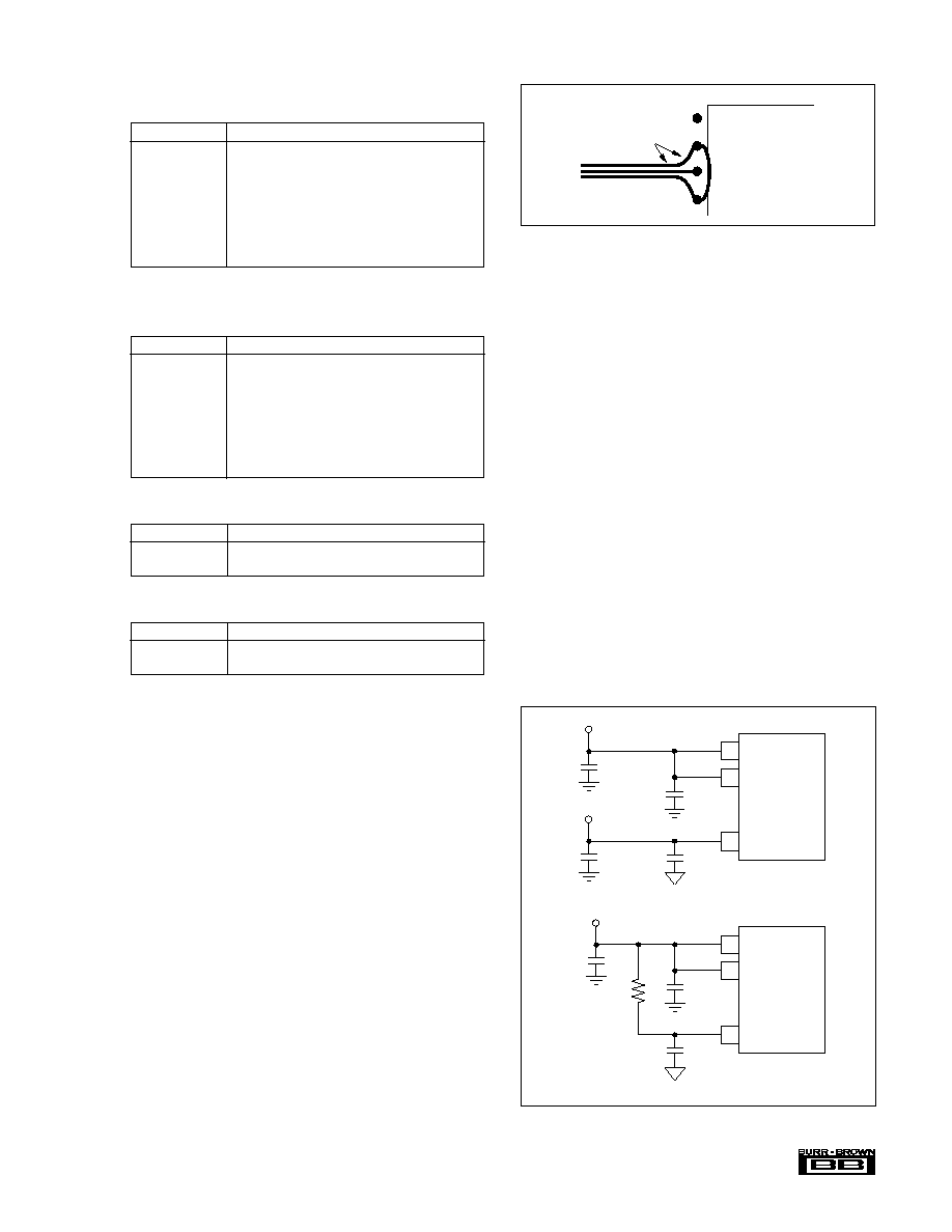
23
DDC101
Æ
Power Supplies
The
±
5VDC supplies of the DDC101 should be bypassed
with 10
µ
F solid tantalum capacitors and 0.1
µ
F ceramic
capacitors. The supplies should each have a 10
µ
F solid
tantalum capacitor at a central point on the PC board. Each
of the DDC101 power supply lines (V
S
+, V
S
≠, V
DD
+) should
have a separate 0.1
µ
F ceramic capacitor placed as close to
the DDC101 package as possible.
The digital power supply voltage, V
DD
+ must be equal to or
less than the analog power supply voltage, V
S
+. The analog
power supply, V
S
+, is connected to pins 5 and 6, these pins
should be hardwired together on the printed circuit board at
the pins for best performance.
V
DD
+ should be as quiet as possible with minimal noise
coupling. It is particularly important to eliminate noise from
V
DD
+ that is non-synchronous with DDC101 operation.
Figure 23 illustrates two acceptable ways to supply V
DD
+
power to the DDC101. The first case shows two separate
+5VDC supplies for V
DD
+ and V
S
+. The second case shows
the V
DD
+ power supply derived from the V
S
+ supply as used
on the DDC101 Evaluation Fixture Device Under Test
(DUT) board.
Oversampling Control
Samples/Integration--M - 4 bits
CODE
SAMPLES PER INTEGRATION
0000
1
0001
2
0010
4
0011
8
0100
16
0101
32
0110
64
0111
128
1XXX
256
SECTION 7
APPLICATIONS INFORMATION
BASIC PRINTED CIRCUIT BOARD LAYOUT
As with any precision circuit, careful printed circuit layout
will ensure best performance. Make short, direct intercon-
nections and avoid stray wiring capacitance--particularly at
the analog input pin. Digital signals should be kept as far
from the analog input signals as possible on the PC board.
Leakage currents between PC board traces can exceed the
input bias current of the DDC101 if care is not taken. A
circuit board "guard" pattern for the analog input pin and for
the PC board trace that connects to the analog input pin is
recommended. The guard pattern reduces leakage effects by
surrounding the analog input pin and trace with a low
impedance analog ground. Leakage currents from other
portions of the circuit will flow harmlessly to the low
impedance analog ground rather than into the analog input
of the DDC101. Analog ground pins are placed on either
side of the analog input pin in the DDC101 package to allow
convenient layout of guard patterns. Figure 22 illustrates the
use of guard patterns to protect the analog input.
Multiple Integration Control
Integrations/Conversion--L - 4 bits
CODE
INTEGRATIONS PER CONVERSION
0000
1
0001
2
0010
4
0011
8
0100
16
0101
32
0110
64
0111
128
1XXX
256
Input Range - 1 bit
CODE
INPUT RANGE
0
Unipolar
1
Bipolar
Output Format - 1 bit
CODE
OUTPUT FORMAT
1
Binary Two's Complement
0
Straight Binary
FIGURE 22. PC Board Layout Showing "Guard" Traces
Surrounding Analog Input Pin and Traces.
5
DDC101
6
12
0.1µF
0.1µF
10
10µF
V
S
+
One +5VDC Supply
5
DDC101
6
12
0.1µF
0.1µF
10µF
V
S
+
Separate +5VDC Supplies
10µF
V
DD
+
FIGURE 23. Positive Supply Connection Options.
DDC101
V
S
≠
Guard
Pattern
Analog Common
Analog Input
Analog Common
Pin 1

Æ
DDC101
24
FIGURE 24. Example of Basic DDC101 Circuit Connections.
Reading Data Output
Data from the previous conversion can be read any time after
the DATA VALID output is activated and before the end of
the next conversion. Data is held in an internal serial shift
register until the end of the next conversion. The data must
be completely read before the end of the next conversion or
it will be overwritten with new data.
Recommended Setup
The following Setup parameters are recommended, in gen-
eral, for use with the DDC101 with integration times of 1ms
or longer. Multiple integrations per conversion, where prac-
tical, will provide lowest noise as illustrated in the typical
performance curves.
Measurement Time Calculation
The time between "Final Data point Start" commands is the
Integration Time, T
INT
. The Measurement Time, T
MEAS
, is the
Integration time reduced by the Acquisition Time and by the
Oversampling Time, T
OS
.
T
MEAS
= T
INT
- T
ACQ
- T
OS
.
When CDS is used; T
OS
, the oversampling time, is the time
required to collect a data point (M clock periods). Each
group of samples is averaged with the result at the midpoint
of each sample group. Therefore, with CDS, T
OS
= M clock
periods. This is shown in Figure 25.
Two calculations of the Measurement Time are shown
A Continuous Integration Cycle consists of the Acquisition
Time, Initial Data Point Collection, Tracking Interval, and
Final Data Point Collection. The user can select these
functions as illustrated in Table XV.
FUNCTION
RECOMMENDED
Acquisition Clocks, K
16
Oversamples, M
128
CDS
Enabled
USER
FUNCTION
CLOCK CYCLES
CONTROLLED
Acquisition Time, K
1, 16, 32
Yes
Initial Data Point
Samples, M
(1)
1, 2, 4, 8, 16, 32,64, 128, 256
Yes
Tracking Interval
Variable
Yes
Final Data Point
Samples, M
(1)
1, 2, 4, 8, 16, 32, 64, 128, 256
Yes
NOTE: (1) Will be the same in CDS mode, initial Data Point Samples = 0 in non-
CDS mode.
TABLE XV. Components of Integration Cycle.
1
2
3
4
5
6
7
8
9
10
11
12
24
23
22
21
20
19
18
17
16
15
14
13
24-Lead SOIC
Top view
+5VDC
0.1µF
0.1µF
0.1µF
≠5VDC
10µF
10µF
Analog Input
10µF
V
REF
Analog Common
Digital Common
Guard
DIGITAL GROUND
V
S
≠
1k
25k
10µF
≠2.5V
REF1004 ≠2.5
10
Reference
Bias
Resistor
Reference
Noise Filter
Reference Buffer Bypass
V
S
≠ , ANALOG
ANALOG COMMON
ANALOG INPUT
ANALOG COMMON
V
S
+, ANALOG
V
S
+, ANALOG
V
DD
+, DIGITAL

25
DDC101
Æ
FIGURE 25. DDC101 Equivalent Integrator Output for Single Integration with CDS.
Input Current Calculation
The following formula calculates the input current from the
actual DDC output:
With CDS:
Without CDS:
below: one with Correlated Double Sampling (CDS) and the
other without CDS. Each example assumes that the recom-
mended system clock frequency of 2MHz is used and that
the time between "Final Data point Start" commands, (the
integration time, T
INT
) is 1ms.
Example with CDS. The Measurement Time with CDS is
calculated as the Integration Time (T
INT
) of 1ms less T
ACQ
and T
OS
. T
OS
, the oversampling time, is 1/2 of the Initial Data
Point time plus 1/2 the Final Data Point time since each
group of samples is averaged with the result at the midpoint
of each sample group.
Therefore, the Measurement Time = 1ms ≠(8 + 32 + 32)
µ
s
= 928
µ
s.
Example without CDS. The Measurement Time without
CDS is calculated as the Total Integration Time (T
INT
) of
1ms less T
ACQ
and T
OS
. T
OS
, the oversampling time, is 1/2 of
the Final Data Point time since this group of samples is
averaged with the result at the midpoint of the sample group.
Therefore, the Measurement Time = 1ms ≠(0.5 + 32)
µ
s
= 967.5
µ
s.
USER SETTING
MEASUREMENT
FUNCTION
(Clock Cycles)
TIME
(Calculated)
Integration Time (T
INT
)
1ms
Acquisition Time K
(T
ACQ
)
16
8
µ
s
Initial Data Point
Samples, M
128
64
µ
s
Measurement Time
928
µ
s
Final Data Point
Samples, M
128
64
µ
s
TABLE XVI. Measurement Time with CDS.
USER SETTING
MEASUREMENT
FUNCTION
(Clock Cycles)
TIME
(Calculated)
Integration Time (T
INT
)
1ms
Acquisition Time, K
(T
ACQ
) "No CDS"
1
0.5
µ
s
Initial Data Point
Samples
None
0
µ
s
Measurement Time
967.5
µ
s
Final Data Point
Samples, M
128
64
µ
s
TABLE XVII. Measurement Time without CDS.
i
=
500pC ∑
DDC output
2
20
T
MEAS
i
=
500pC ∑
DDC output
2
20
T
MEAS
i
=
500pC ∑
DDC output
2
20
T
INT
≠ K clock periods ≠ M / 2 clock periods
i
=
500pC ∑
DDC output
2
20
T
INT
≠ K clock periods ≠ M clock periods
X
X
Measurement Time
Digital
Output
M
Aquisition
Time, K
Oversampled
Initial Data Point
N
Tracking Interval
Time
Clock
Cycles
Final Data
Point Start
M
Oversampled
Final Data Point
DDC101 digital output is precise integration of input during measurement time.
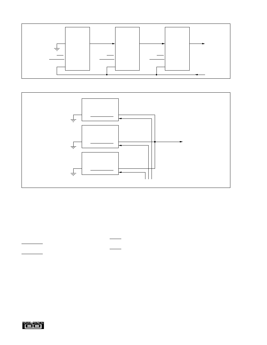
Æ
DDC101
26
FIGURE 26. Daisy Chained DDC101s.
FIGURE 27. DDC101 Parallel Operation.
MULTIPLE DDC101 OPERATION
Multiple DDC101 units can be connected in serial or parallel
configuration as illustrated in Figures 26 and 27.
DATA OUTPUT can be used with DATA INPUT to "daisy
chain" the output of several DDC101 units together to
minimize wiring; in this mode of operation, the serial data
output is shifted through multiple DDC101s (Figure 26).
DATA OUTPUT is in a high impedance state until DATA
TRANSMIT In is active. In this way, several DDC101 units
can be connected in parallel to be enabled by the DATA
TRANSMIT In line (Figure 27).
DDC101 EVALUATION FIXTURE
The DEM-DDC101P-C Evaluation Fixture is highly recom-
mended for initial evaluation of the DDC101. It is designed
for ease of use. The only additional equipment required to do
a complete evaluation of the performance of the DDC101 is
an IBM compatible PC with EGA or VGA graphics, a
parallel interface port, a laser printer (optional), a
±
5VDC
power supply, and a signal source.
The DEM-DDC101P-C software is mouse compatible and
retrieves data from up to 32 DDC101s in an easy to read,
graphical format on the screen. The DEM-DDC101P-C
Evaluation Fixture includes a PC Interface Board (with
necessary parts), a DDC101 Board, a 25-pin ribbon connec-
tor and a 34-pin ribbon connector. The PC Interface Board
makes timing commands and access to and from the DDC101
test board possible through the provided PC software. Data
sheet, LI-439, provides complete information describing the
evaluation fixture.
DATA
INPUT
DDC101
Data Output
DATA OUTPUT
DATA TRANSMIT In
DATA
INPUT
DDC101
DATA OUTPUT
DATA TRANSMIT In
DATA
INPUT
DDC101
DATA OUTPUT
DATA TRANSMIT In
Enable
DATA
INPUT
DATA
OUTPUT
DATA
TRANSMIT
In
DDC101
DDC101
DATA
INPUT
DATA
OUTPUT
DATA
INPUT
DATA
OUTPUT
DATA
TRANSMIT
In
DATA
TRANSMIT
In
DDC101
27
DDC101
Æ
FIGURE 28. Photo of DEM-DDC101P-C Evaluation Fixture.
Your PC
25 Pin Cable
34 Pin Cable
+5VDC
±5VDC
DUT Board Assembly
Analog Input
PC Interface Board
Power Supply
FIGURE 29. DEM-DDC101P-C Evaluation Fixture Connection Diagram.