 | ÐлекÑÑоннÑй компоненÑ: DF1704E | СкаÑаÑÑ:  PDF PDF  ZIP ZIP |
Äîêóìåíòàöèÿ è îïèñàíèÿ www.docs.chipfind.ru
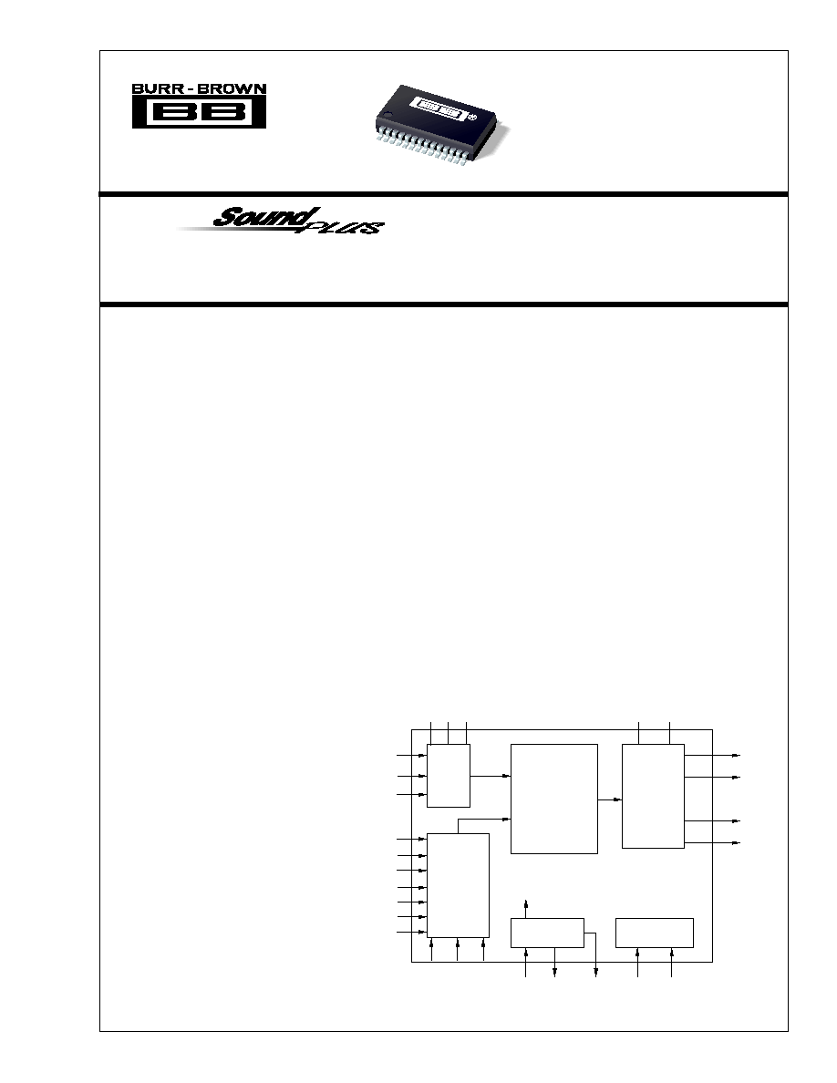
Stereo, 24-Bit, 96kHz
8X Oversampling Digital Interpolation Filter
DIGITAL-TO-ANALOG CONVERTER
49%
FPO
DF1704
®
TM
DESCRIPTION
The DF1704 is a high performance, stereo, 8X
oversampling digital interpolation filter designed for
high-end consumer and professional audio applica-
tions. The DF1704 supports 24-bit, 96kHz operation
and features user-programmable functions, including
selectable filter response, de-emphasis, attenuation,
and input/output data formats.
The DF1704 is the ideal companion for Burr-Brown's
PCM1704 24-bit audio digital-to-analog converter.
This combination allows for construction of very high
performance audio systems and components.
FEATURES
q
COMPANION DIGITAL FILTER FOR THE
PCM1704 24-BIT AUDIO DAC
q
HIGH PERFORMANCE FILTER:
Stopband Attenuation: 115dB
Passband Ripple:
±
0.00005dB
q
AUDIO INTERFACE:
Input Data Formats: Standard, Left-
Justified, and I
2
S
Input Word Length: 16, 20, or 24 Bits
Output Word Length: 16, 18, 20, or 24 Bits
Sampling Frequency: 32kHz to 96kHz
q
SYSTEM CLOCK: 256f
S
, 384f
S
, 512f
S
, 768f
S
q
ON-CHIP CRYSTAL OSCILLATOR
q
PROGRAMMABLE FUNCTIONS:
Hardware or Software Control Modes
Sharp or Slow Roll-Off Filter Response
Soft Mute
Digital De-Emphasis
Independent Left/Right Digital Attenuation
q
+5V SINGLE-SUPPLY OPERATION
q
SMALL 28-LEAD SSOP PACKAGE
© 1998 Burr-Brown Corporation
PDS-1458B
Printed in U.S.A. December, 1998
DF1704
Serial
Input
I/F
Mode
Control
I/F
8X Oversampling
Digital Filter with
Function
Controller
Crystal/OSC
XTI
SCK
XTO
CLKO
(SF0) (SF1) (SRO)
V
DD
V
SS
Output I/F
BCKO
(I
2
S)
(IW1)
(IW0)
(OW1)
(OW0)
WCKO
DOL
DOR
MC/LRIP
MD/CKO
LRCIN
DIN
BCKIN
MODE
ML/RESV
(MUTE)
RST
(DEM)
Power Supply
International Airport Industrial Park · Mailing Address: PO Box 11400, Tucson, AZ 85734 · Street Address: 6730 S. Tucson Blvd., Tucson, AZ 85706 · Tel: (520) 746-1111
Twx: 910-952-1111 · Internet: http://www.burr-brown.com/ · Cable: BBRCORP · Telex: 066-6491 · FAX: (520) 889-1510 · Immediate Product Info: (800) 548-6132
®
2
DF1704
SPECIFICATIONS
All specifications at +25
°
C, V
DD
= +5V, unless otherwise noted.
DF1704E
PARAMETER
CONDITIONS
MIN
TYP
MAX
UNITS
RESOLUTION
24
Bits
INPUT DATA FORMAT
Audio Data Interface Format
Standard /Left-Justified /I
2
S
Audio Data Bit Length
16/20/24 Selectable
Audio Data Format
MSB-First, Two's Binary Comp
Sampling Frequency (f
S
)
32
96
kHz
System Clock Frequency
256/384/512/768f
S
OUTPUT DATA FORMAT
Audio Data Interface Format
Right-Justified
Audio Data Bit Length
16 /20/24 Selectable
Audio Data Format
MSB-First, Binary Two's Complement
DIGITAL INPUT/OUTPUT
Input Logic Level:
V
IH
2.0
V
V
IL
0.8
V
Output Logic Level: V
OH
I
OH
= 2mA
4.5
V
V
OL
I
OL
= 4mA
0.5
V
CLKO AC CHARACTERISTICS
Rise Time (t
R
)
20% to 80% V
DD
, 10pF
4
ns
Fall Time
(t
F
)
80% to 20% V
DD
, 10pF
3
ns
Duty Cycle
10pF Load
37
%
DIGITAL FILTER PERFORMANCE
Filter Characteristics 1 (Sharp Roll-Off)
Passband
±
0.00005dB
0.454f
S
3dB
0.493f
S
Stopband
0.546f
S
Passband Ripple
±
0.00005
dB
Stopband Attenuation
Stopband = 0.546f
S
115
dB
Filter Characteristics 2 (Sharp Roll-Off)
Passband Ripple
±
0.0001dB
0.254f
S
3dB
0.460f
S
Stopband
0.732f
S
Passband Ripple
±
0.0001
dB
Stopband Attenuation
Stopband = 0.748f
S
100
dB
Delay Time
45.125/f
S
sec
De-Emphasis Error
±
0.003
dB
POWER SUPPLY REQUIREMENTS
Voltage Range
V
DD
4.5
5
5.5
VDC
Supply Current: I
DD
20
30
mA
Power Dissipation
100
150
mW
TEMPERATURE RANGE
Operation
25
+85
°
C
Storage
55
+100
°
C
®
3
DF1704
PIN
NAME
I/O
DESCRIPTION
1
DIN
IN
Serial Audio Data Input
(3)
2
BCKIN
IN
Bit Clock Input for Serial Audio Data
(3)
3
I
2
S
IN
Input Audio Data Format Selection
(2, 4)
4
IW0
IN
Input Audio Data Word Selection
(2, 4)
5
IW1
IN
Input Audio Data Word Selection
(2, 4)
6
XTI
IN
Oscillator Input /External Clock Input
7
XTO
OUT
Oscillator Output
8
V
SS
--
Digital Ground
9
CLKO
OUT
Buffered System Clock Output
10
MODE
IN
Mode Control Selection (H: Software, L: Hardware)
(1)
11
MD/CKO
IN
Control Data Input/Clock Output Frequency
Select
(1, 5)
12
MC/LRIP
IN
Control Data Clock/Polarity of LRCK Select
(1, 5)
13
ML/RESV
IN
Control Data Latch/Reserved
(1, 5)
14
RST
IN
Reset. When this pin is LOW, the digital filter
is held in reset.
(1)
15
MUTE
IN
Mute Control
(1, 4)
16
DEM
IN
De-Emphasis Control
(2, 4)
17
SF0
IN
Sampling Rate Select for De-emphasis
(2, 4)
18
SF1
IN
Sampling Rate Select for De-emphasis
(2, 4)
19
OW0
IN
Output Audio Data Word and Format Select
(2, 4)
20
OW1
IN
Output Audio Data Word and Format Select
(2, 4)
21
NC
--
No Connection
22
V
DD
--
Digital Power, +5V
23
DOR
OUT
Rch, Serial Audio Data Output
24
DOL
OUT
Lch, Serial Audio Data Output
25
WCKO
OUT
Word Clock for Serial Audio Data Output
26
BCKO
OUT
Bit Clock for Serial Audio Data Output
27
SRO
IN
Filter Response Select
(2, 4)
28
LRCIN
IN
L/R Clock Input (f
S
) for Serial Audio Data
(3)
NOTES: (1) Pins 10-15; Schmitt-Trigger input with pull-up resistor. (2) Pins
3-5, 16-20, 27; Schmitt-Trigger input with pull-down resister. (3) Pins 1, 2,
28; Schmitt-Trigger input. (4) Pins 3-5, 15-20, 27; these pins are invalid
when MODE (pin 10) is HIGH. (5) Pins 11-13; these pins have different
functions corresponding to MODE (pin 10), (HIGH/LOW).
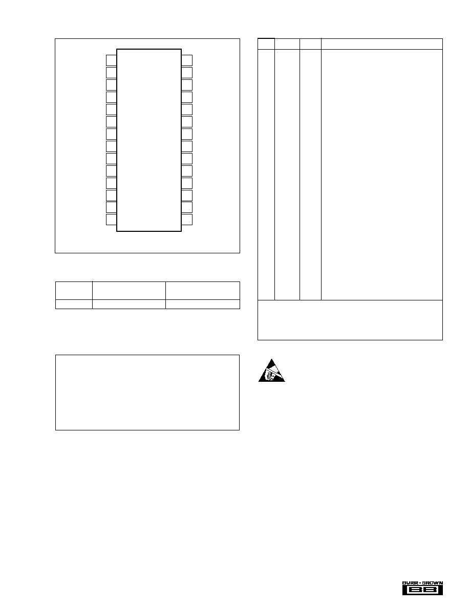
PIN ASSIGNMENTS
PIN CONFIGURATION
PACKAGE DRAWING
PRODUCT
PACKAGE
NUMBER
(1)
DF1704E
28-Lead SSOP
324
NOTE: (1) For detailed drawing and dimension table, please see end of data
sheet, or Appendix C of Burr-Brown IC Data Book.
PACKAGE INFORMATION
ELECTROSTATIC
DISCHARGE SENSITIVITY
This integrated circuit can be damaged by ESD. Burr-Brown
recommends that all integrated circuits be handled with
appropriate precautions. Failure to observe proper handling
and installation procedures can cause damage.
ESD damage can range from subtle performance degradation
to complete device failure. Precision integrated circuits may
be more susceptible to damage because very small parametric
changes could cause the device not to meet its published
specifications.
The information provided herein is believed to be reliable; however, BURR-BROWN assumes no responsibility for inaccuracies or omissions. BURR-BROWN assumes
no responsibility for the use of this information, and all use of such information shall be entirely at the user's own risk. Prices and specifications are subject to change
without notice. No patent rights or licenses to any of the circuits described herein are implied or granted to any third party. BURR-BROWN does not authorize or warrant
any BURR-BROWN product for use in life support devices and/or systems.
Supply Voltage (V
DD
, V
CC
1, V
CC
2R, V
CC
2L) .................................... +6.5V
Supply Voltage Differences .................................................................
±
0.1
GND Voltage Differences ..................................................................
±
0.1V
Digital Input Voltage ................................................. 0.3V to (V
DD
+ 0.3V)
Input Current (any pins except power supplies) .............................
±
10mA
Power Dissipation .......................................................................... 300mW
Operating Temperature Range ......................................... 25
°
C to +85
°
C
Storage Temperature ...................................................... 55
°
C to +125
°
C
Lead Temperature (soldering, 5s) ................................................. +260
°
C
Package Temperature (reflow, 10s) .............................................. +235
°
C
ABSOLUTE MAXIMUM RATINGS
DIN
BCKIN
I
2
S
IW0
IW1
XTI
XTO
V
SS
CLKO
MODE
MD/CKO
MC/LRIP
ML/RESV
RST
LRCIN
SRO
BCKO
WCKO
DOL
DOR
V
DD
NC
OW1
OW0
SF1
SF0
DEM
MUTE
1
2
3
4
5
6
7
8
9
10
11
12
13
14
28
27
26
25
24
23
22
21
20
19
18
17
16
15
DF1704E
NC: No Connection
®
4
DF1704
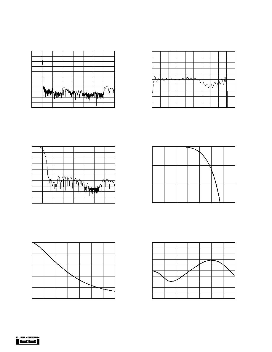
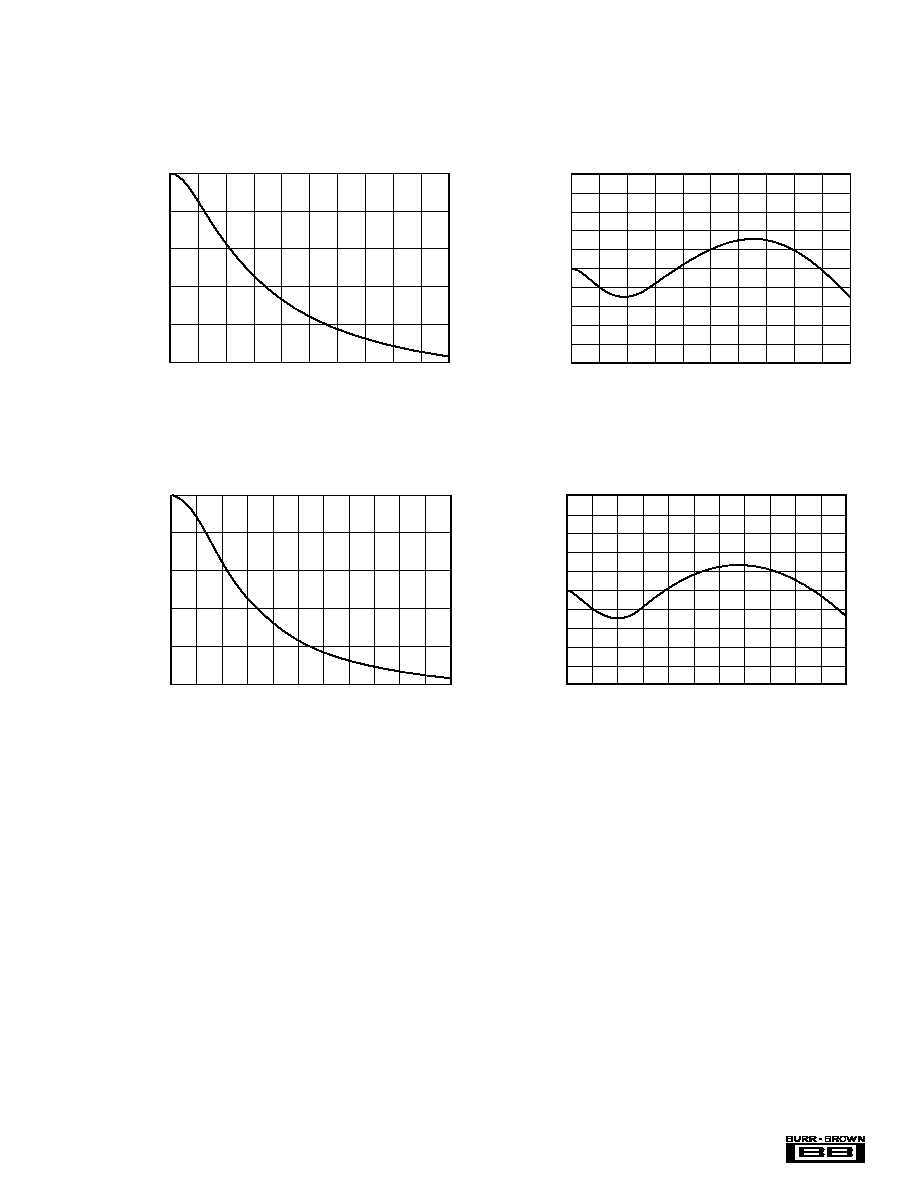
TYPICAL PERFORMANCE CURVES OF INTERNAL FILTER
DIGITAL FILTER (DE-EMPHASIS OFF, f
S
= 44.1kHz)
DE-EMPHASIS AND DE-EMPHASIS ERROR
0
4
3.5
3
2.5
2
1.5
1
0.5
Frequency (f
S
)
20
0
20
40
60
80
100
120
140
160
180
200
FREQUENCY RESPONSE (Sharp Roll Off)
Attenuation (dB)
0
0.5
0.45
0.4
0.3
0.35
0.25
0.2
0.15
0.1
0.5
Frequency (f
S
)
0.0001
0.00008
0.00006
0.00004
0.00002
0
0.00002
0.00004
0.00006
0.00008
0.0001
PASSBAND RIPPLE (Sharp Roll Off)
Attenuation (dB)
0
4
3.5
3
2.5
2
1.5
1
0.5
Frequency (f
S
)
0
20
40
60
80
100
120
140
160
180
200
FREQUENCY RESPONSE (Slow Roll Off)
Attenuation (dB)
0
0.1
0.2
0.3
0.4
0.5
0.7
0.6
Frequency (f
S
)
TRANSITION CHARACTERISTIC (Slow Roll Off)
0
5
10
15
Attenuation (dB)
0
14
12
10
8
6
4
2
Frequency ( f
S
)
0
2
4
6
8
10
DE-EMPHASIS (f
S
= 32kHz)
Level (dB)
0
14
12
8
10
6
4
2
Frequency (f
S
)
0.01
0.008
0.006
0.004
0.002
0
0.002
0.004
0.006
0.008
0.01
DE-EMPHASIS ERROR (f
S
= 32kHz)
Error (dB)
®
5
DF1704
TYPICAL PERFORMANCE CURVES OF INTERNAL FILTER
0
20
18
16
10
14
12
8
6
4
2
Frequency (f
S
)
0
2
4
6
8
10
DE-EMPHASIS (f
S
= 44.1kHz)
Level (dB)
0
20
18
16
10
14
12
8
6
4
2
Frequency (f
S
)
DE-EMPHASIS ERROR (f
S
= 44.1kHz)
0.01
0.008
0.006
0.004
0.002
0
0.002
0.004
0.006
0.008
0.01
Error (dB)
0
22
20
18
16
10
14
12
8
6
4
2
Frequency (f
S
)
0
2
4
6
8
10
DE-EMPHASIS (f
S
= 48kHz)
Level (dB)
0
22
20
18
16
10
14
12
8
6
4
2
Frequency (f
S
)
DE-EMPHASIS ERROR (f
S
= 48kHz)
0.01
0.008
0.006
0.004
0.002
0
0.002
0.004
0.006
0.008
0.01
Error (dB)
®
6
DF1704
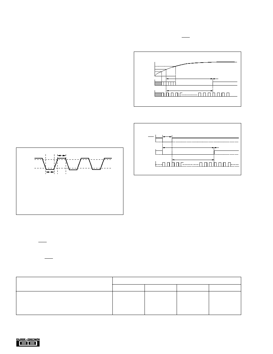
RESET
The DF1704 has both an internal power-on reset circuit and
a reset pin, RST (pin 14), for providing an external reset
signal. The internal power-on reset is performed automati-
cally when power is applied to the DF1704, as shown in
Figure 2. The RST pin can be used to synchronize the
DF1704 with a system reset signal, as shown in Figure 3.
SYSTEM CLOCK REQUIREMENTS
The system clock of the DF1704 can be supplied by either
an external clock signal at XTI (pin 6), or by the on-chip
crystal oscillator. The system clock rate must run at 256f
S
,
384f
S
, 512f
S
, or 768f
S
, where f
S
is the audio sampling rate.
It should be noted that a 768f
S
system clock cannot be used
when f
S
= 96kHz. In addition, the on-chip crystal oscillator
is limited to a maximum frequency of 24.576MHz. Table I
shows the typical system clock frequencies for selected
sample rates.
The DF1704 includes a system clock detection circuit that
determines the system clock rate in use. The circuit com-
pares the system clock input (XTI) frequency with the
LRCIN input rate to determine the system clock multiplier.
Ideally, LRCIN and BCKIN should be derived from the
system clock to ensure proper synchronization. If the phase
difference between the system clock and LRCIN is larger
than
±
6 bit clock (BCKIN) periods, the synchronization of
the system and LRCIN clocks will be performed automati-
cally by the DF1704.
Timing requirements for the system clock input are shown in
Figure 1.
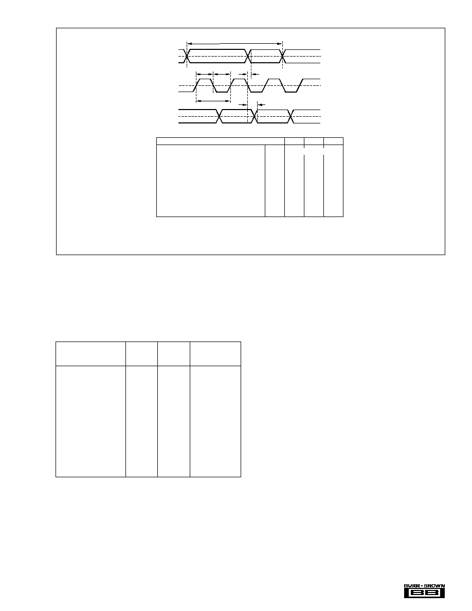
AUDIO INPUT INTERFACE
The audio input interface is comprised of BCKIN (pin 2),
LRCIN (pin 28), and DIN (pin 1).
BCKIN is the input bit clock, which is used to clock data
applied at DIN into the DF1704's input serial interface.
Input data at DIN is clocked into the DF1704 on the rising
edge of BCKIN. The left/right clock, LRCIN, is used as a
word latch for the audio input data.
BCKIN can run at 32f
S
, 48f
S
, or 64f
S
, where f
S
is the audio
sample frequency. LRCIN is run at the f
S
rate. Figures 4 (a)
through 4 (c) show the input data formats, which are sel-
ected by hardware or software controls. Figure 5 shows the
audio input interface timing requirements.
SYSTEM CLOCK FREQUENCY (MHz)
SAMPLING RATE FREQUENCY (f
S
)
256f
S
384f
S
512f
S
768f
S
32kHz
8.1920
12.2880
16.3840
24.5760
44.1kHz
11.2896
16.9340
22.5792
33.8688
(1)
48kHz
12.2880
18.4320
24.5760
36.8640
(1)
96kHz
24.5760
(3)
36.8640
(1)
49.1520
(1)
See Notes 1, 2
NOTES: (1) Maximum crystal oscillator frequency is 24.576MHz and cannot be used for these combinations. (2) 768f
S
system clock cannot be used with 96kHz
sampling rate. (3) Use external system clock applied at XTI.
TABLE I. Typical System Clock Frequencies.
FIGURE 1. System Clock Timing.
1024 system clocks
Reset
Reset Removal
V
DD
2.2V
2.6V
1.8V
Internal Reset
System Clock
FIGURE 2. Internal Power-On Reset Timing.
FIGURE 3. External Forces Reset Timing.
t
SCKH
System Clock Pulse Width HIGH
:t
SCKIH
:7ns min
(1)
System Clock Pulse Width LOW
:t
SCKIL
:7ns min
(1)
t
SCKL
2.0V
0.8V
"H"
"L"
XTI
NOTE: (1) For f
S
= 96kHz and SCK = 256f
S
, t
SCKIH
= 14ns (min)
t
SCKIL
= 14ns (min)
For f
S
96kHz and SCK = 256f
S
, t
SCKIH
= 20ns (min)
t
SCKIL
= 20ns (min)
1024 system (XTI) clocks
Reset
Reset Removal
System Clock
Internal Reset
RST
t
RST
t
RST
20ns
During the power-on reset period (1024 system clocks), the
DF1704 outputs are forced LOW. For an external forced
reset, the outputs are forced LOW during the initialization
period (1024 system clocks), which occurs after the LOW-
to-HIGH transition of the RST pin as shown in Figure 3.
®
7
DF1704
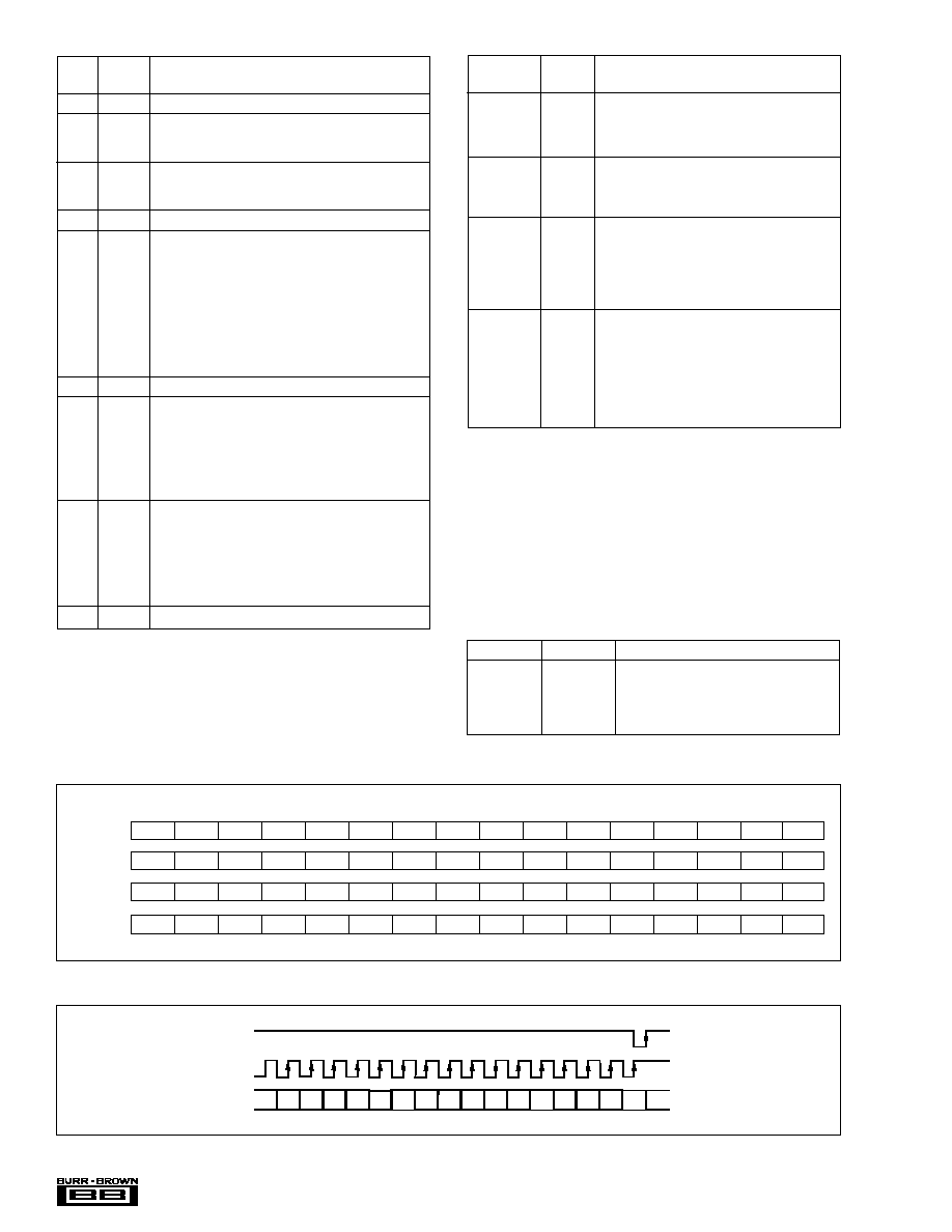
FIGURE 5. Audio Input Interface Timing.
FIGURE 4. Audio Data Input Formats.
LRCKIN
BCKIN
DIN
1.4V
1.4V
1.4V
t
BCH
t
BCL
t
LB
t
BL
t
DS
BCKIN Pulse Cycle Time
BCKIN Pulse Width HIGH
BCKIN Pulse Width LOW
BCKIN Rising Edge to LRCIN Edge
LRCIN Edge to BCKIN Rising Edge
DIN Set-up Time
DIN Hold Time
t
BCY
t
BCH
t
BCL
t
BL
t
LB
t
DS
t
DH
100ns (min)
50ns (min)
50ns (min)
30ns (min)
30ns (min)
30ns (min)
30ns (min)
t
DH
t
BCY
1
2
3
22
23
1/f
S
Lch
Rch
MSB
LSB
24
LRCIN
BCKIN
AUDIO DATA WORD = 24-BIT
DIN
1
2
3
1
2
3
22
23
MSB
LSB
24
(b) Left-Justified Format; Lch = "H", Rch = "L"
1
2
15
1/f
S
Lch
Rch
MSB
LSB
16
LRCIN
BCKIN
AUDIO DATA WORD = 16-BIT
DIN
1
2
15
MSB
LSB
16
2
1
2
1
1
2
23
MSB
LSB
24
AUDIO DATA WORD = 24-BIT
DIN
1
2
23
MSB
LSB
24
(c) I
2
S Data Format (Philips Format); Lch = "L", Rch = "H"
14
15
16
1
2
15
1/f
S
Lch
Rch
MSB
LSB
16
LRCIN
BCKIN
AUDIO DATA WORD = 16-BIT
(a) Standard Format (Sony Format); Lch = "H", Rch = "L"
DIN
1
2
15
16
18
19
22
23
20
1
2
19
MSB
LSB
20
AUDIO DATA WORD = 20-BIT
DIN
1
2
19
20
24
1
2
23
MSB
LSB
24
AUDIO DATA WORD = 24-BIT
DIN
1
2
23
MSB
LSB
24
®
8
DF1704
14
15
16
1
2
1/8f
S
MSB
LSB
WCKO
BCKO
AUDIO DATA WORD = 16-BIT
DOR
DOL
15
16
18
19
22
23
20
1
2
MSB
LSB
AUDIO DATA WORD = 20-BIT
DOR
DOL
19
20
24
1
2
MSB
LSB
AUDIO DATA WORD = 24-BIT
DOR
DOL
23
24
16
17
18
1
2
MSB
LSB
AUDIO DATA WORD = 18-BIT
DOR
DOL
17
18
(a) SYSTEM CLOCK: 256/512f
S
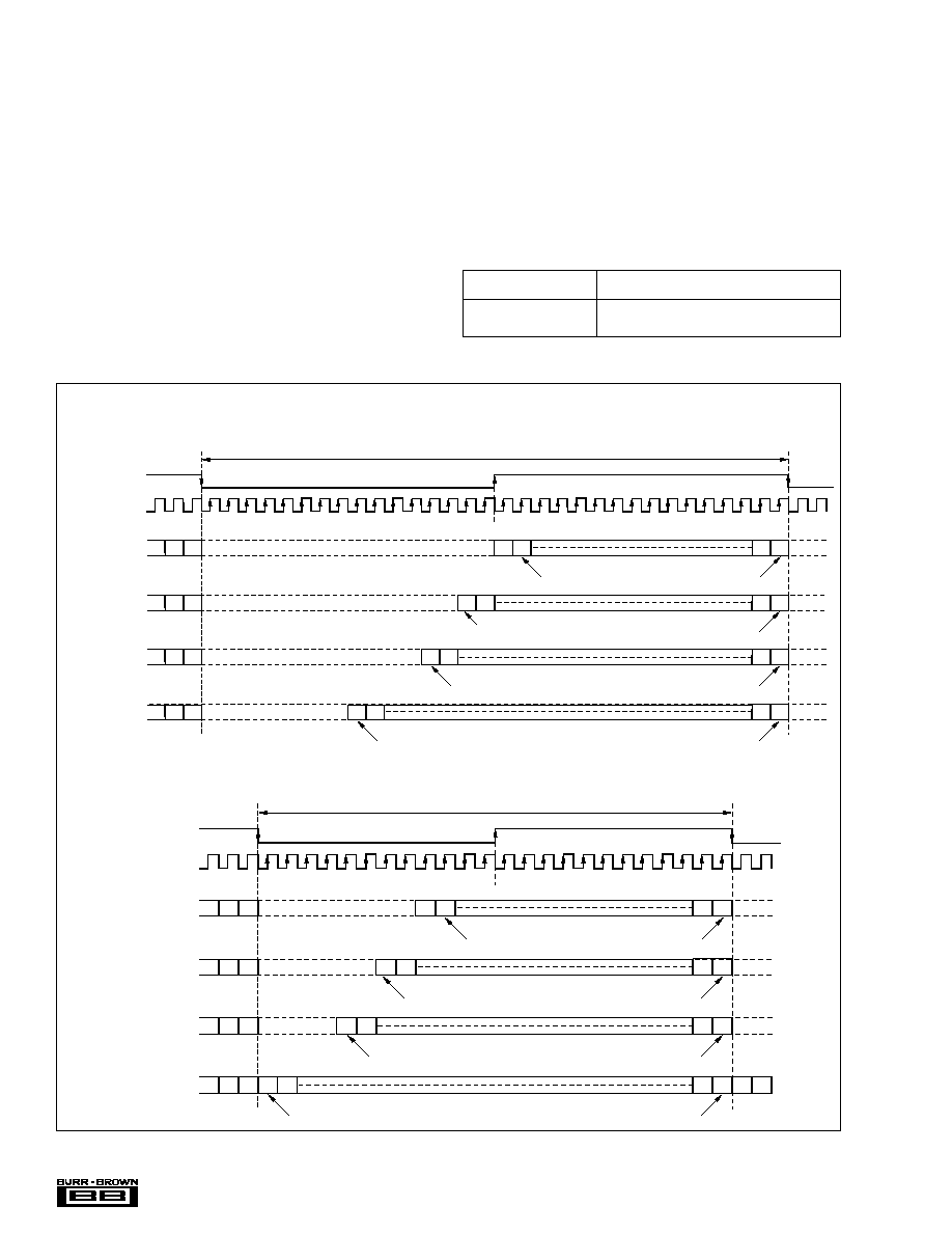
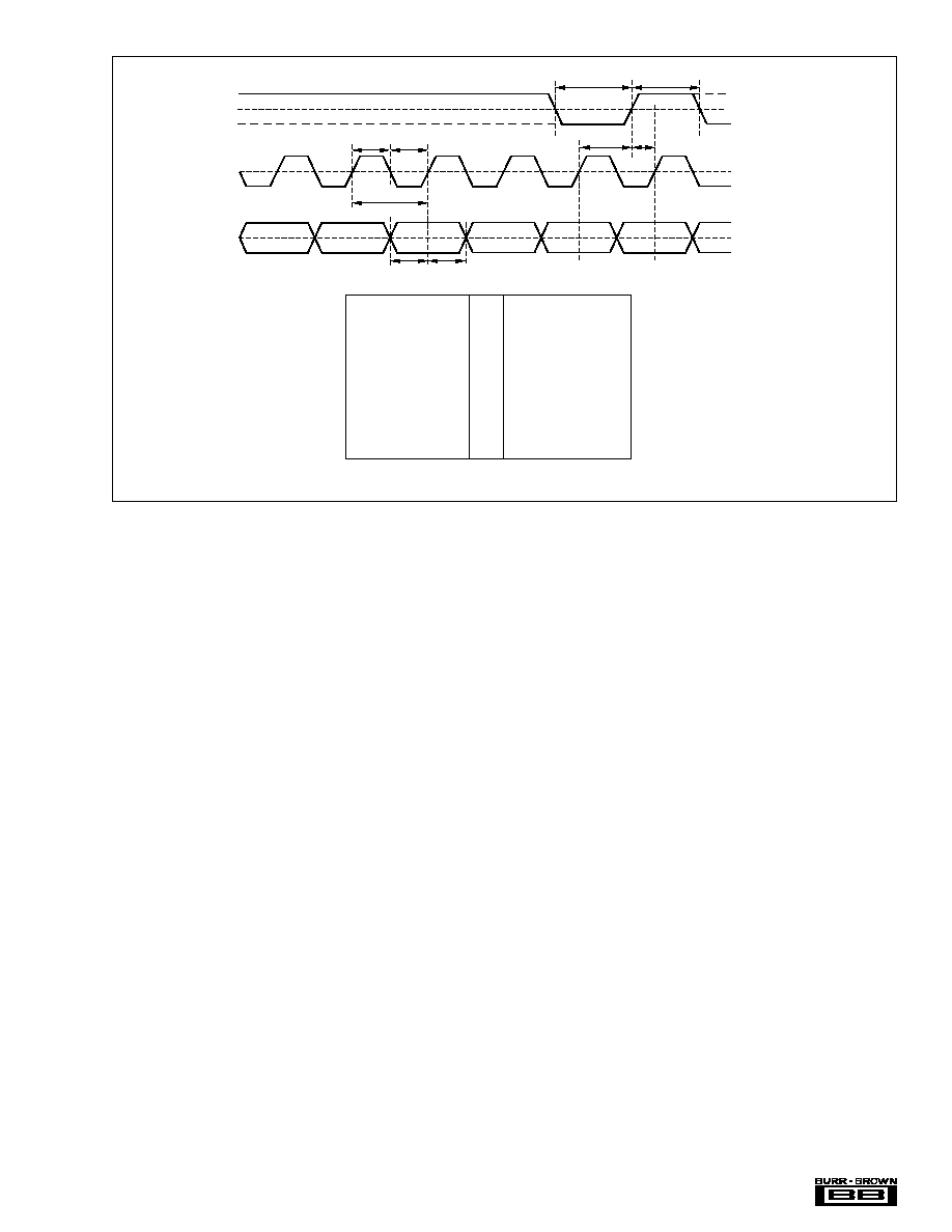
AUDIO OUTPUT INTERFACE
The audio output interface includes BCKO (pin 26), WCKO
(pin 25), DOL (pin 24), and DOR (pin 23).
BCKO is the output bit clock and is used to clock data into
an audio D/A converter, such as the PCM1704. DOL and
DOR are the left and right audio data outputs. WCKO is the
output word clock and is used to latch audio data words into
an audio D/A converter.
WCKO runs at a fixed rate of 8f
S
(8X oversampling) for all
system clock rates.
BCKO is fixed at 256f
S
for system clock rates of 256f
S
or
512f
S
.
BCKO is fixed at 192f
S
for system clock rates of 384f
S
or
768f
S
.
The output data format used by the DF1704 for DOL and
DOR is Binary Two's Complement, MSB-first, right-justi-
fied audio data. Figures 6(a) and 6(b) show the output data
formats for the DF1704. Figure 7 shows the audio output
timing.
MODE CONTROL
The DF1704 may be configured using either software or
hardware control. The selection is made using the MODE
input (pin 10).
TABLE II. MODE Selection.
MODE SETTING
MODE CONTROL SELECTION
MODE = H
Software Mode
MODE = L
Hardware Mode
FIGURE 6. Audio Output Data Format.
14
15
16
1
2
1/8f
S
MSB
LSB
WCKO
BCKO
AUDIO DATA WORD = 16-BIT
DOR
DOL
MSB
15
16
18
19
22
23
20
1
2
MSB
LSB
AUDIO DATA WORD = 20-BIT
DOR
DOL
19
20
24
1
2
MSB
LSB
AUDIO DATA WORD = 24-BIT
DOR
DOL
23
24
1
2
16
17
18
1
2
LSB
AUDIO DATA WORD = 18-BIT
DOR
DOL
17
18
(b) SYSTEM CLOCK: 384/768f
S
®
9
DF1704
RESET
SOFTWARE
HARDWARE
DEFAULT
FUNCTION
(MODE = H)
(MODE = L)
(Software Mode)
Input Data Format Selection
O
O
Standard Format
Input Word Length Selection
O
O
16 Bits
Output Word Length Selection
O
O
16 Bits
LRCIN Polarity Selection
O
O
Left/Right = High/Low
Digital De-Emphasis
O
O
OFF
Soft Mute
O
O
OFF
Digital Attenuation
O
X
0dB, Independent L/R
Sample Rate for
De-Emphasis Function
O
O
44.1 kHz
Filter Roll-Off Selection
O
O
Sharp Roll-Off Selected
CLKO Output Frequency Selection
O
O
Same As XTI Input
Legend:
O
= User Programmable, X = Not Available.
TABLE III. User-Programmable Functions for Software and
Hardware Mode.
Programmable Functions
The DF1704 includes a number of programmable features,
with most being accessible from either Hardware or Soft-
ware mode. Table III summarizes the user programmable
functions for both modes of operation.
Hardware Mode Controls
With MODE = L, the DF1704 may be configured by
utilizing several user-programmable pins. The following is a
brief summary of the pin functions. Table IV provides more
details on setting the hardware mode controls.
Pins I
2
S, IW0, and IW1 are used to select the audio data
input format and word length.
Pins OW0 and OW1 are used to select the output data word
length.
The DEM pin is used to enable and disable the digital de-
emphasis function. De-emphasis is only available for 32kHz,
44.1kHz, and 48kHz sample rates.
Pins SF0 and SF1 are used to select the sample rate for the
de-emphasis function.
The SRO pin is used to select the digital filter response,
either sharp or slow roll-off.
The MUTE pin is used to enable or disable the soft mute
function.
The CKO pin is used to select the clock frequency seen at the
CLKO pin, either XTI or XTI
÷
2.
The LRIP pin is used to select the polarity used for the audio
input left/right clock, LRCIN.
Finally, the RESV pin is not used by the current DF1704
design, but is reserved for future use.
Software Mode Controls
With MODE = H, the DF1704 may be configured by
programming four internal registers in software mode. ML
(pin 13), MC (pin 12), and MD (pin 11) make up the 3-wire
software control port, and may be controlled using DSP or
microcontroller general purpose I/O pins, or a serial port.
Table V provides an overview of the internal registers,
labeled MODE0 through MODE3.
t
BCKH
0.5V
DD
0.5V
DD
BCKO
DOL, R
t
BCKL
t
CKWK
t
WCKP
t
BCKP
t
CKDO
0.5V
DD
WCKO
BCKO Period
BCKO Pulse Width High
(4)
BCKO Pulse Width Low
(4)
Delay Time BCKO Falling Edge to WCKO Valid
WCKO Period
Delay Time BCKO Falling Edge to DOL, R Valid
Rising Time of All Signals
Falling Time of All Signals
t
BCKP
t
BCKH
t
BCKL
t
CKWK
t
WCKP
t
CKDO
t
R
t
F
min
typ
1/8 f
S
20ns
20ns
5ns
5ns
100ns
100ns
5ns
5ns
7ns
7ns
max
1/256 f
S
or 1/192 f
S
NOTES: (1) Timing measurement reference level is (V
IH
/V
IL
)/2. (2) Rising and falling time is
measured from 10% to 90% of IN/OUT signals' swing. (3) Load capacitance of all signals
are 20pF. (4) Exceptions: f
S
= 96kHz and SCK = 256f
S
, t
BCKH
= 14ns (min)
t
BCKL
= 14ns (min)
FIGURE 7. Audio Output Data Format.
®
10
DF1704
Figures 8 through 10 show more details regarding the
control port data format and timing requirements. The data
format for the control port is 16-bit, MSB-first, with Bit B15
being the MSB.
B15
B14
B13
B12
B11
B10
B9
B8
B7
B6
B5
B4
B3
B2
B1
B0
MODE0
res
res
res
res
res
A1
A0
LDL
AL7
AL6
AL5
AL4
AL3
AL2
AL1
AL0
MODE1
res
res
res
res
res
A1
A0
LDR
AR7
AR6
AR5
AR4
AR3
AR2
AR1
AR0
MODE2
res
res
res
res
res
A1
A0
res
res
OW1
OW0
IW1
IW0
res
DEM
MUT
MODE3
res
res
res
res
res
A1
A0
res
SF1
SF0
CKO
res
SRO
ATC
LRP
I
2
S
B15 B14 B13 B12 B11 B10 B9 B8 B7 B6 B5 B4 B3 B2 B1 B0
ML
MC
MD
FIGURE 8. Internal Mode Control Registers.
FIGURE 9. Software Interface Format.
PIN
PIN
NAME
NUMBER
DESCRIPTION
RESV
13
Reserved, Not Used
LRIP
12
LRCIN Polarity
LRIP = H: LRCIN= H = Left Channel, LRCIN= L = Right Channel
LRIP = L: LRCIN= L = Left Channel, LRCIN = H = Right Channel
CKO
11
CLKO Output Frequency
CKO = H: CLKO Frequency = XTI/2
CKO = L: CLKO Frequency = XTI
MUTE
15
Soft Mute Control: H = Mute Off, L = Mute On
I
2
S
3
Input Data Format Controls
IW0
4
IW1
5
I
2
S
IW1
IW0
INPUT FORMAT
L
L
L
16-Bit, Standard, MSB-First, Right-Justified
L
L
H
20-Bit, Standard, MSB-First, Right-Justified
L
H
L
24-Bit, Standard, MSB-First, Right-Justified
L
H
H
24-Bit, MSB-First, Left-Justified
H
L
L
16-Bit, I
2
S
H
L
H
24-Bit, I
2
S
SRO
27
Digital Filter Roll-Off: H = Slow, L = Sharp
OW0
19
Output Data Word Length Controls
OW1
20
OW1 OW0
OUTPUT FORMAT
L
L
16-Bit, MSB-First
L
H
18-Bit, MSB-First
H
L
20-Bit, MSB-First
H
H
24-Bit, MSB-First
SF0
17
Sample Rate Selection for the Digital De-Emphasis Control
SF1
18
SF1
SF0
SAMPLING RATE
L
L
44.1kHz
L
H
Reserved, Not Used
H
L
48kHz
H
H
32kHz
DEM
16
Digital De-Emphasis: H = On, L = Off
TABLE IV. Hardware Mode Controls.
REGISTER
BIT
NAME
NAME
DESCRIPTION
MODE0
AL[7:0]
Attenuation Data for the Left Channel
LDL
Attenuation Load Control for the Left Channel
A[1:0]
Register Address
res
Reserved
MODE1
AR[7:0]
Attenuation Data for the Right Channel
LDL
Attenuation Load Control for the Right Channel
A[1:0]
Register Address
res
Reserved
MODE2
MUT
Soft Mute Control
DEM
Digital De-Emphasis Control
IW[1:0]
Input Data Format and Word Length
OW[1:0]
Output Data Word Length
A[1:0]
Register Address
res
Reserved
MODE3
I
2
S
Input Data Format (I
2
S or Standard/Left-Justified)
LRP
LRCIN Polarity
ATC
Attenuator Control, Dependent or Independent
SRO
Digital Filter Roll-Off Selection (sharp or slow)
CKO
CLKO Frequency Selection (XTI or XTI
÷
2)
SF[1:0]
Sample Rate Selection for De-Emphasis Function
A[1:0]
Register Address
res
Reserved
NOTE: All reserved bits should be programmed to 0.
TABLE V. Internal Register Mapping.
Register Addressing
A[1:0], bits B10 and B9 of the 16-bit control data word, are
used to indicate the register address to be written to by the
current control port write cycle. Table VI shows how to
address the internal registers using bits A[1:0] of registers
MODE0 through MODE3.
A1
A0
REGISTER SELECTED
0
0
MODE0
0
1
MODE1
1
0
MODE2
1
1
MODE3
TABLE VI. Internal Register Addressing.
®
11
DF1704
FIGURE 10. Software Interface Timing Requirements.
1.4V
1.4V
1.4V
ML
(1)
MC
(2)
MD
NOTES: (1) ML rising edge to the next MC rising edge. (2) MC rising edge for LSB to ML rising edge. (3) SYSCK: System Clock Cycle.
t
MLH
t
MHH
t
MCH
t
MCL
t
MDS
t
MCY
t
MLS
t
MLL
t
MDH
LSB
MC Pulse Cycle Time
MC Pulse Width LOW
MC Pulse Width HIGH
MD Hold Time
MD Set-Up Time
ML Low Level Time
ML High Level Time
ML Hold Time
(2)
ML Set-Up Time
(3)
t
MCY
t
MCL
t
MCH
t
MDH
t
MDS
t
MLL
t
MHH
t
MLH
t
MLS
100ns (min)
40ns (min)
40ns (min)
40ns (min)
40ns (min)
40ns + 1SYSCLK
(3)
(min)
40ns + 1SYSCLK
(3)
(min)
40ns (min)
40ns (min)
MODE0 Register
The MODE0 register is used to set the attenuation data for
the Left output channel, or DOL (pin 24).
When ATC = 1 (Bit B2 of Register MODE3 = 1), the Left
channel attenuation data AL[7:0] is used for both the Left
and Right channel attenuators.
When ATC = 0, (Bit B2 of Register MODE3 = 0), Left
channel attenuation data is taken from AL[7:0] of register
MODE0, and Right channel attenuation data is taken from
AR[7:0] of register MODE1.
AL[7:0]
Left Channel Attenuator Data, where AL7 is the
MSB and AL0 is the LSB.
Attenuation Level is given by:
ATTEN = 0.5 · (DATA 255)dB
For DATA = FFh, ATTEN = 0dB
For DATA = FEh, ATTEN = 0.5dB
For DATA = 01h, ATTEN = 127.5dB
For DATA = 00h, ATTEN = infinity = Mute
LDL
Left Channel Attenuation Data Load Control.
This bit is used to simultaneously set attenua-
tion levels of both the Left and Right channels.
When LDL = 1, the Left channel output level is
set by the data in AL[7:0]. The Right channel
output level is set by the data in AL[7:0], or the
most recently programmed data in bits AR[7:0]
of register MODE1.
When LDL = 0, the Left channel output data
remains at its previously programmed level.
MODE1 Register
The MODE1 register is used to set the attenuation data for
the Right output channel, or DOR (pin 23).
When ATC = 1 (Bit B2 of Register MODE3 = 1), the Left
channel attenuation data AL[7:0] of register MODE0 is used
for both the Left and Right channel attenuators.
When ATC = 0, (Bit B2 of Register MODE3 = 0), Left
channel attenuation data is taken from AL[7:0] of register
MODE0, and Right channel attenuation data is taken from
AR[7:0] of register MODE1.
AR[7:0]
Right Channel Attenuator Data, where AR7 is
the MSB and AR0 is the LSB. Attenuation
Level is given by:
ATTEN = 0.5 · (DATA 255)dB
For DATA = FFh, ATTEN = 0dB
For DATA = FEh, ATTEN = 0.5dB
For DATA = 01h, ATTEN = 127.5dB
For DATA = 00h, ATTEN = infinity = Mute
LDR
Right Channel Attenuation Data Load Control.
This bit is used to simultaneously set attenuation
levels of both the Left and Right channels.
When LDR = 1, the Right channel output level
is set by the data in AR[7:0], or by the data in
bits AL[7:0] of register MODE0. The Left chan-
nel output level is set to the most recently
programmed data in bits AL[7:0] of register
MODE0.
When LDR = 0, the Right channel output data
remains at its previously programmed level.

®
12
DF1704
MODE2 Register
The MODE2 register is used to program various functions:
MUT
Soft Mute Function.
When MUT = 0, Soft Mute is ON for both Left
and Right channels.
When MUT = 1, Soft Mute is OFF for both Left
and Right channels.
DEM
Digital De-Emphasis Function.
When DEM = 0, de-emphasis is OFF.
When DEM = 1, de-emphasis is ON.
IW[1:0]
Input Data Format and Word Length.
I
2
S
IW1
IW0
Description
0
0
0
16-Bit Data, Standard
Format (MSB-First,
Right-Justified)
0
0
1
20-Bit Data, Standard
Format
0
1
0
24-Bit Data, Standard
Format
0
1
1
24-Bit Data, MSB-First,
Left-Justified
1
0
0
16-Bit Data, I
2
S Format
1
0
1
24-Bit Data, I
2
S format
1
1
0
Reserved
1
1
1
Reserved
OW[1:0]
Output Data Word Length.
OW1 OW0
Description
0
0
16-Bit Data, MSB-First
0
1
18-Bit Data, MSB-First
1
0
20-Bit Data, MSB-First
1
1
24-Bit Data, MSB-First
MODE3 Register
The MODE3 register is used to program various functions.
I
2
S
Input Data Format.
When I
2
S = 0, standard or left-justified formats
are enabled.
When I
2
S = 1, the I
2
S formats are enabled.
LRP
LRCIN Polarity Selection.
When LRP = 0, Left channel is HIGH and Right
channel is LOW.
When LRP = 1, Left channel is LOW and Right
channel is HIGH.
ATC
Attenuator Control.
This bit is used to determine whether the Left
and Right channel attenuators operate with inde-
pendent data, or use common data (the Left
channel data in bits AL[7:0] of register MODE0).
When ATC = 0, the Left and Right channel
attenuator data is independent.
When ATC = 1, the Left and Right channel
attenuators use common data.
SRO
Digital Filter Roll-Off Selection.
When SRO = 0, sharp roll-off is selected.
When SRO = 1, slow roll-off is selected.
CKO
CLKO Output Frequency Selection.
When CKO = 0, the CLKO frequency is the
same as the clock at the XTI input.
When CKO =1, the CLKO frequency is half of
the XTI input clock frequency.
SF[1:0]
Sampling Frequency Selection for the De-Em-
phasis Function.
SF1 SF0
Description
0
0
44.1 kHz
0
1
Reserved
1
0
48 kHz
1
1
32 kHz
APPLICATIONS INFORMATION
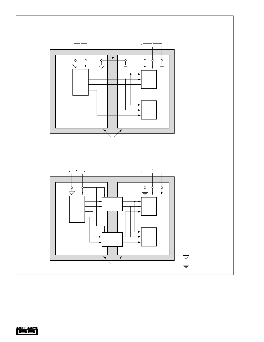
PCB LAYOUT GUIDELINES
In order to obtain the specified performance from the DF1704
and its associated D/A converters, proper printed circuit
board layout is essential. Figure 11 shows two approaches
for obtaining the best audio performance.
Figure 11(a) shows a standard, mixed signal layout scheme.
The board is divided into digital and analog sections, each
with its own ground. The ground areas should be put on a
split-plane, separate from the routing and power layers. The
DF1704 and all digital circuitry should be placed over the
digital section, while the audio DACs and analog circuitry
should be located over the analog section of the board. A
common connection between the digital and analog grounds
is required and is done at a single point as shown.
For Figure 11(a), digital signals should be routed from the
DF1704 to the audio DACs using short, direct connections
to reduce the amount of radiated high-frequency energy. If
necessary, series resistors may be placed in the clock and
data signal paths to reduce or eliminate any overshoot or
undershoot present on these signals. A value of 50
to 100
is recommended as a starting point, but the designer should
experiment with the resistor values in order to obtain the best
results.

®
13
DF1704
Figure 11(b) shows an improved method for high perfor-
mance, mixed signal board layout. This method adds digital
isolation between the DF1704 and the audio DACs, and
provides complete isolation between the digital and analog
sections of the board. The Burr-Brown ISO150 dual digital
coupler provides excellent isolation, and operates at speeds
up to 80Mbps.
POWER SUPPLIES AND BYPASSING
The DF1704 requires a single +5V power supply for opera-
tion. The power supply should be bypassed by a 10
µ
F and
0.1
µ
F parallel capacitor combination. The capacitors should
be placed as close as possible to V
DD
(pin 22). Aluminum
electrolytics or tantalum capacitors can be used for the 10
µ
F
value, while ceramics may be used for the 0.1
µ
F value.
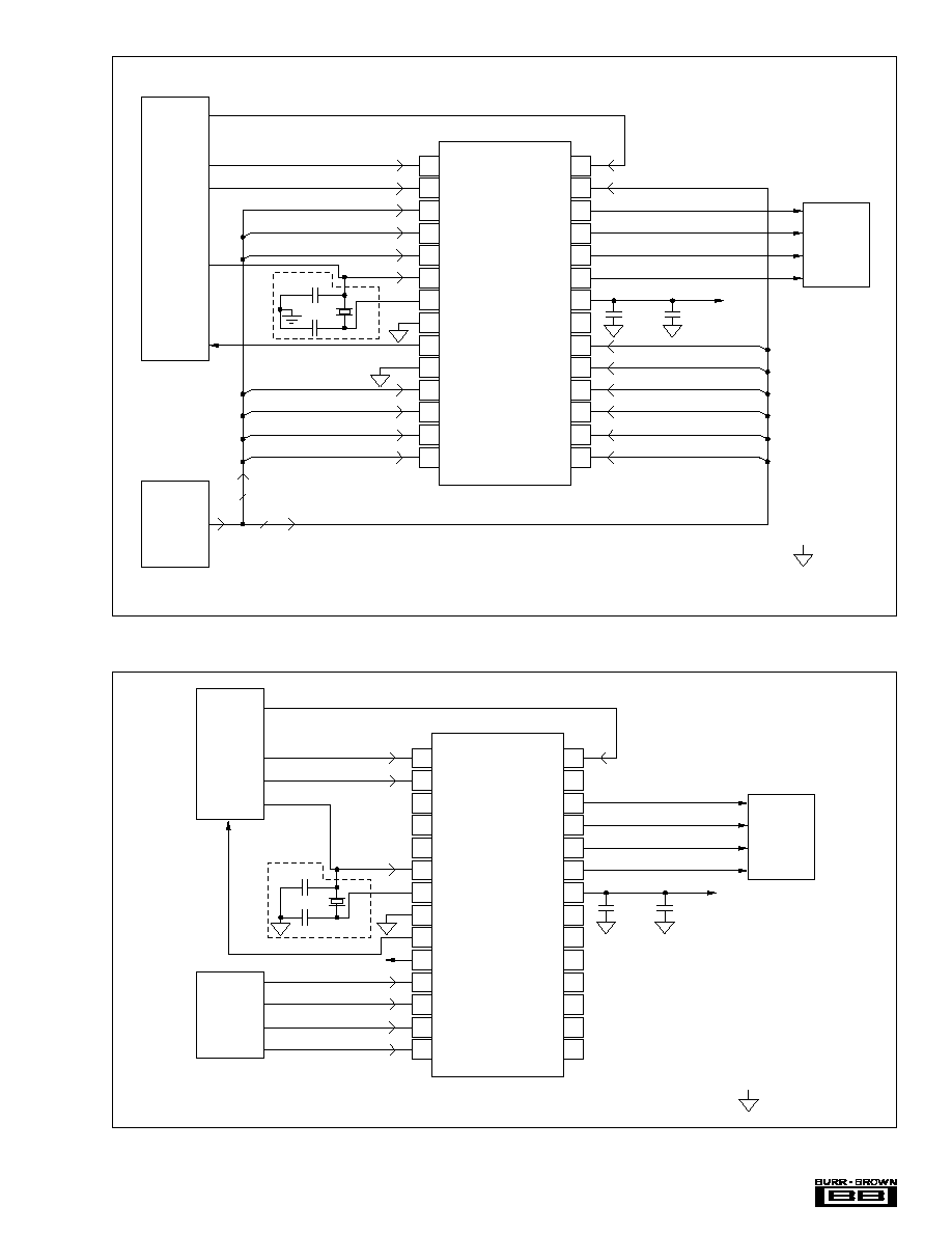
BASIC CIRCUIT CONNECTIONS
Figures 12 and 13 show basic circuit connections for the
DF1704. Figure 12 shows connections for Hardware mode
controls, while Figure 13 shows connections for Software
mode controls. Notice the placement of C
1
and C
2
in both
figures, as they are physically close to the DF1704.
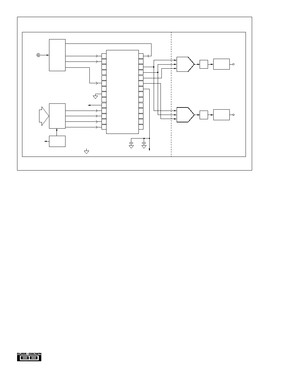
TYPICAL APPLICATIONS
The DF1704 will typically be used in high performance
audio equipment, in conjunction with high performance
audio D/A converters. Figure 14 shows a typical application
circuit example, employing the DF1704, a digital audio
receiver, and two PCM1704 24-bit, 96kHz audio DACs.
®
14
DF1704
FIGURE 11. PCB Layout Model.
Analog Power
Supplies
Common
Ground
Connection
DAC
DF1704
Digital Section
Analog Section
WCKO
BCKO
DOL
DOR
DAC
Split Ground Plane
(a) Layout Without Isolation
Digital Power
Supplies
Analog Power
Supplies
DAC
DF1704
Digital Section
Analog Section
WCKO
BCKO
DOL
DOR
ISO150
DAC
Split Ground Plane
(b) Layout With Isolation
Digital Power
Supplies
ISO150
= DGND
= AGND
®
15
DF1704
FIGURE 12. Basic Circuit Connections, Hardware Control.
FIGURE 13. Basic Circuit Connection, Software Control.
1
2
3
4
5
6
7
8
9
10
11
12
13
14
DIN
BCKIN
I
2
S
IWO
IW1
XTI
XTO
V
SS
CLKO
MODE
MD
MC
ML
RST
28
27
26
25
24
23
22
21
20
19
18
17
16
15
LRCIN
SRO
BCKO
WCKO
DOL
DOR
V
DD
NC
OW1
OW0
SF1
SF0
DEM
MUTE
DF1704
Controller
or
Logic
+5V
(optional)
XTAL
D/A
Converters
or
Digital
Couplers
C
2
10
µ
F
+5V
+
C
1
0.1
µ
F
Audio
Data
and
Clock
Source
22pF
22pF
= DGND
1
2
3
4
5
6
7
8
9
10
11
12
13
14
DIN
BCKIN
I
2
S
IW0
IW1
XTI
XTO
V
SS
CLKO
MODE
MD/CKO
MC/LRIP
ML/RESV
RST
28
27
26
25
24
23
22
21
20
19
18
17
16
15
LRCIN
SRO
BCKO
WCKO
DOL
DOR
V
DD
NC
OW1
OW0
SF1
SF0
DEM
MUTE
DF1704
Digital
Logic
or
Manual
Controls
NOTE: Do not allow pins 3-5, 11-20, and 27 to float. These pins should be manually
connected to V
DD
or DGND (hardwired, switch, jumper) or actively driven by logic.
(optional)
XTAL
D/A
Converters
or
Digital
Couplers
+5V
+
C
1
0.1
µ
F
C
2
10
µ
F
Audio
Data
and
Clock
Source
22pF
22pF
7
7
= DGND
®
16
DF1704
FIGURE 14. DF1704 Typical Application Circuit.
1
2
3
4
5
6
7
8
9
10
11
12
13
14
DIN
BCKIN
I
2
S
IWO
IW1
XTI
XTO
V
SS
CLKO
MODE
MD
MC
ML
RST
28
27
26
25
24
23
22
21
20
19
18
17
16
15
LRCIN
SRO
BCKO
WCKO
DOL
DOR
V
DD
NC
OW1
OW0
SF1
SF0
DEM
MUTE
DF1704
PCM1704
Micro
Controller
or
Logic
Host
Interface
System
Reset
+5V
+5V
Post
Filter
I/V
10
µ
F
+
0.1
µ
F
+5V
Digital
Audio
Receiver
Digital
Audio
Input
WORD CLOCK
DATA
BIT CLOCK
SYSTEM CLOCK
D/A
Converter
ANALOG
SECTION
DIGITAL
SECTION
BCLK
WCLK
DATA
PCM1704
Post
Filter
I/V
D/A
Converter
BCLK
WCLK
DATA
Left
Channel
Out
Right
Channel
Out
= DGND