 | ÐлекÑÑоннÑй компоненÑ: DF1760U | СкаÑаÑÑ:  PDF PDF  ZIP ZIP |
Äîêóìåíòàöèÿ è îïèñàíèÿ www.docs.chipfind.ru
FEATURES
q
DUAL 20-BIT MONOLITHIC MODULATOR
(PCM1760) AND MONOLITHIC
DECIMATING DIGITAL FILTER (DF1760)
q
HIGH PERFORMANCE:
THD+N: 92dB typ, 90dB max
Dynamic Range: 108dB typ
SNR: 108dB min, 110dB typ
Channel Separation: 98dB typ, 94dB min
q
64X OVERSAMPLING
q
CO-PHASE CONVERSION
q
RUNS ON 256fs OR 384fs SYSTEM
CLOCK
q
VERSATILE INTERFACE CAPABILITY:
16-, 20-Bit Output
MSB First or LSB First Format
q
OPTIONAL FUNCTIONS:
Offset Error Calibration
Overflow Detection
Power Down Mode (DF1760)
q
RUNS ON
±
5V SUPPLIES (PCM1760) AND
5V SUPPLY (DF1760)
q
COMPACT 28-PIN PACKAGES:
28-Pin DIP and SOIC
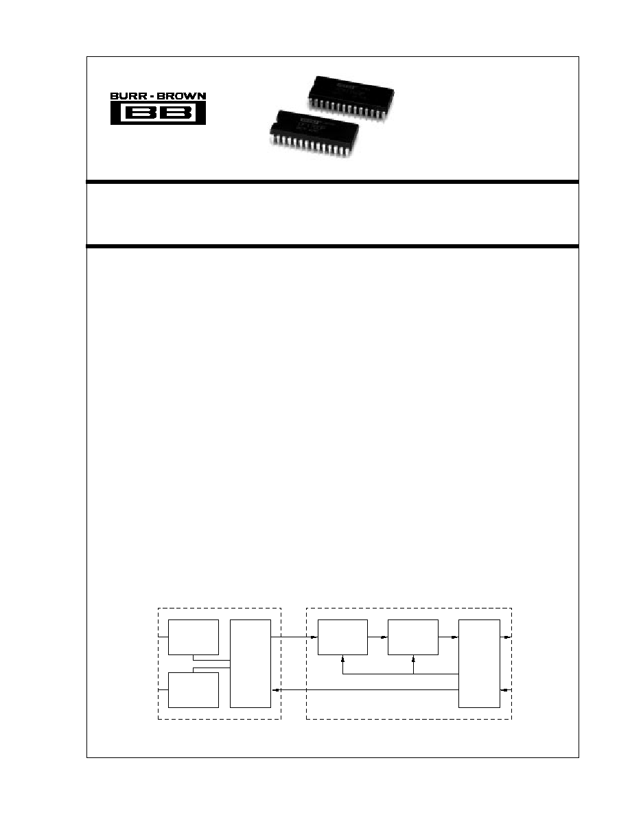
Multi-Bit Enhanced Noise Shaping 20-Bit
ANALOG-TO-DIGITAL CONVERSION SYSTEM
DESCRIPTION
The PCM1760 and DF1760 combine for a low-cost,
high-performance dual 20-bit, 48kHz sampling ana-
log-to-digital conversion system which is specifically
designed for dynamic applications.
The PCM1760/DF1760 pair form a 4-bit, 4th order,
64X oversampling analog-to-digital converter.
The PCM1760 is a delta-sigma modulator that uses a
4-bit quantizer within the modulation loop to achieve
very high dynamic range.
The DF1760 is a high-performance decimating digital
filter. The DF1760 accepts 4-bit 64fs data from the
PCM1760 and decimates to 20-bit 1fs data.
The FIR filter of the DF1760 has pass-band ripple of
less than
±
0.001dB and greater than 100dB of the
reject band attenuation.
4 Stage, 4-Bit
Delta-Sigma
Modulator
4 Stage, 4-Bit
Delta-Sigma
Modulator
Timing
Control
and
Interface
1/16
Filter
FIR
Filter
Timing
Control
and
Interface
PCM1760
Analog
Input (L)
Analog
Input (R)
64fs
256fs
4fs
fs
Data
System
Clock
256/384fs
64fs
DF1760
International Airport Industrial Park · Mailing Address: PO Box 11400 · Tucson, AZ 85734 · Street Address: 6730 S. Tucson Blvd. · Tucson, AZ 85706
Tel: (520) 746-1111 · Twx: 910-952-1111 · Cable: BBRCORP · Telex: 066-6491 · FAX: (520) 889-1510 · Immediate Product Info: (800) 548-6132
PCM1760P/U
DF1760P/U
®
©
1993 Burr-Brown Corporation
PDS-1174C
Printed in U.S.A. July, 1994
®
PCM1760P/U DF1760P/U
2
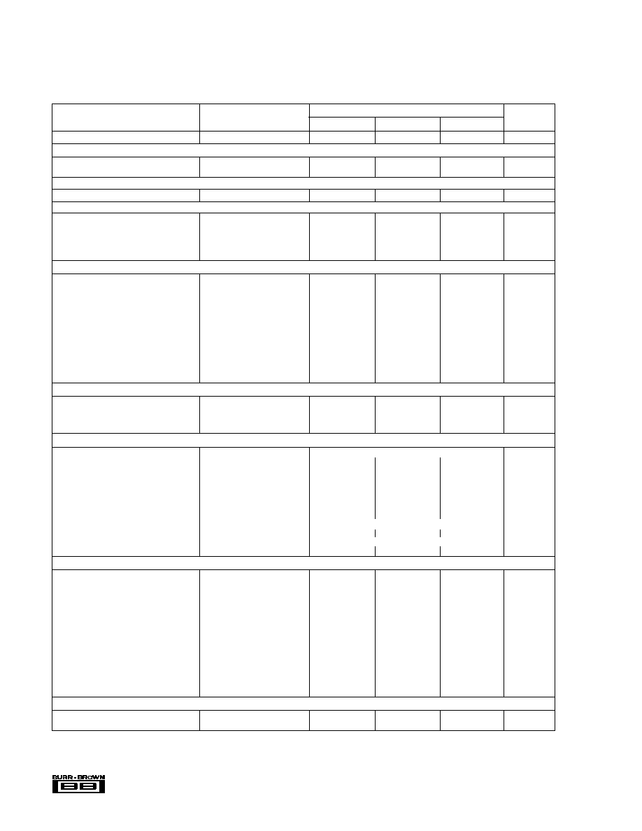
SPECIFICATIONS
ELECTRICAL
At T
A
= +25
°
C,
±
V
CC
,
±
V
dd
= +5V, +V
DD
= +5V, f
S
= 48kHz and ext. components =
±
2% unless otherwise noted.
PCM1760/DF1760
PARAMETER
CONDITIONS
MIN
TYP
MAX
UNITS
RESOLUTION
20
Bits
ANALOG INPUT
Input Range
R
IN
1 = 2.2k
±
2.5
Vp-p
Input Impedance
R
IN
1 = 2.2k
R
IN
1
SAMPLING FREQUENCY
Cover Range of fs
Integrator Constants: Application
(1)
30
48
50
kHz
ACCURACY
Gain Error
±
0.5
±
1.0
dB
Gain Mismatch
±
0.5
dB
Bipolar Zero Error
V
IN
= 0 at 20s After Power-On
±
0.4
% FSR
(2)
Gain Drift
0
°
C to +70
°
C
±
100
ppmfs/
°
C
Bipolar Zero Drift
0
°
C to +70
°
C
±
20
ppmfs/
°
C
DYNAMIC CHARACTERISTICS
(4)
THD+N/(0dBFS)
P, U
f
IN
= 1kHz
92
90
dB
P-L, U-L
90
88
dB
THD+N/(20dBFS)
P, U
f
IN
= 1kHz
76
70
dB
P-L, U-L
76
70
dB
THD+N/(60dBFS)
P, U
f
IN
= 1kHz
44
42
dB
P-L, U-L
44
42
dB
Dynamic Range
P, U
f
IN
= 1kHz, V
IN
= 60dBFS, A Filter
104
108
dB
P-L, U-L
104
108
dB
SNR
P, U
V
IN
= 0, A Filter
108
110
dB
P-L, U-L
106
110
dB
Frequency Response
f
IN
= 20kHz
±
0.1
dB
Channel Separation
f
IN
= 1kHz, A Filter
94
98
dB
DIGITAL FILTER
Over Sample Rate
64
fs
Ripple in Band
0 - 0.04535fs
±
0.0001
dB
Stopband Attenuation 1
0.5465fs - 63.4535fs
94
dB
Stopband Attenuation 2
0.5465fs - 3.4535fs
100
dB
LOGIC INPUTS AND OUTPUTS
Logic Family Input
TTL Level Compatible CMOS
Frequency (System Clock 1)
256fs
12.288
MHz
Frequency (System Clock 2)
384fs
18.432
MHz
Duty Cycle (System Clock 1)
256fs
40
50
60
%
Duty Cycle (System Clock 2)
384fs
45
50
55
%
Data Clock Input
32
48
64
fs
Logic Family Output
CMOS
Data Clock Output
64
fs
Data Coding
Two's Complement
Data Bit Length
16
20
Bits
Data Format
Selectable
Output Data Delay
fs = 48kHz
1.5
ms
POWER SUPPLY REQUIREMENTS
Supply Voltage
±
V
CC
PCM1760
±
4.75
±
5.0
±
5.25
V
±
V
dd
PCM1760
±
4.75
±
5.0
±
5.25
V
+V
DD
DF1760
4.75
5.0
5.25
V
Supply Current
+I
CC
PCM1760
24
36
mA
I
CC
PCM1760
30
45
mA
+I
dd
PCM1760
12
18
mA
I
DD
PCM1760
8
12
mA
+I
DD
1
DF1760, Normal Mode
40
55
mA
+I
DD
2
DF1760, Power-Down Mode
4
6.6
mA
Power Consumption
PCM1760
370
500
mW
DF1760, Normal Mode
200
275
mW
DF1760, Power-Down Mode
20
33
mW
TEMPERATURE RANGE
Operating
PCM1760/DF1760
0
+25
+70
°
C
Storage
PCM1760/DF1760
50
+125
°
C
NOTES: (1) Integrator Constants are determined by the external components shown in the block diagram. (2) FSR means Full Scale Range, digital output code is from
90000H to 70000H, FSR = 5.0V. (3) Use 20-bit DAC, 20kHz LPF, 400Hz HPF, average response. (4) Average response using a 20-bit reconstruction DAC with 20kHz
low-pass filter and 400Hz high-pass filter.
®
3
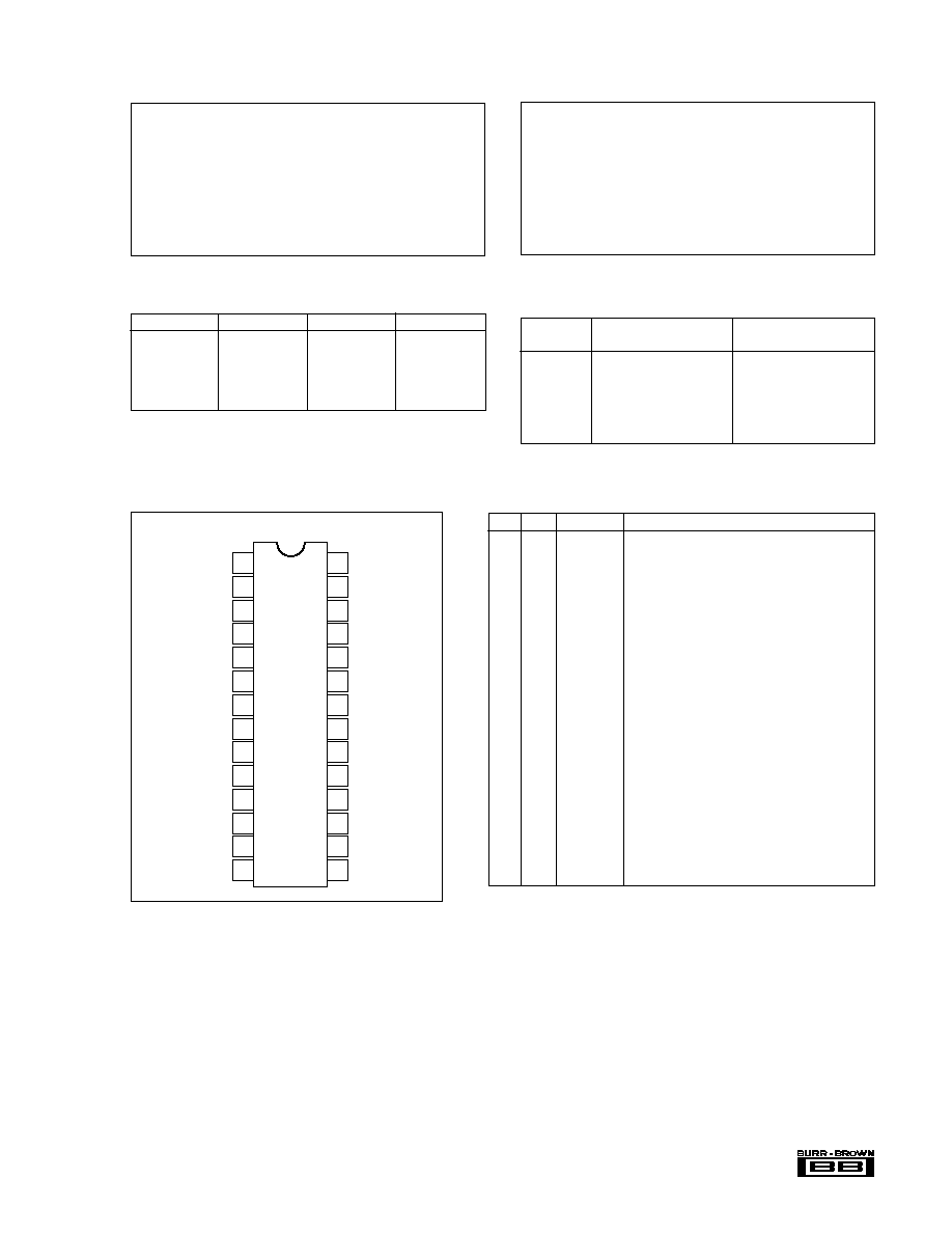
PCM1760P/U DF1760P/U
MODEL
PACKAGE
THD +N (fs)
SNR
PCM1760P
PDIP
90dB
108dB
PCM1760U
SOIC
90dB
108dB
PCM1760P-L
PDIP
88dB
106dB
PCM1760U-L
SOIC
88dB
106dB
DF1760P
PDIP
NA
NA
DF1760U
SOIC
NA
NA
Supply Voltage .................................................................................... 7.0V
Voltage Mismatch ............................................................................... 0.1V
Digital Input ............................................................................... +V
DD
+0.5V
V
SS
0.5V
Input Current
±
20mA
Power Dissipation/P ....................................................................... 460mW
Power Dissipation/U ....................................................................... 440mW
Lead Temperature/P (soldering, 10s) .............................................. 260
°
C
Lead Temperature/U (soldering, 10s, reflow) ................................... 235
°
C
Operating Temperature .......................................................... 0
°
C to +70
°
c
Storage Temperature ...................................................... 50
°
C to +125
°
C
Supply Voltage .....................................................................................
±
6V
Voltage Mismatch ............................................................................... 0.1V
Analog Input ........................................................................................
±
V
CC
Digital Input ............................................................................... +V
DD
+0.3V
GND 0.3V
Power Dissipation/P ....................................................................... 580mW
Power Dissipation/U ....................................................................... 550mW
Lead Temperature/P (soldering, 10s) .............................................. 260
°
C
Lead Temperature/U (soldering, 10s) .............................................. 235
°
C
Operating Temperature ......................................................... 0
°
C to +70
°
C
Storage Temperature ...................................................... 50
°
C to +125
°
C
ABSOLUTE MAXIMUM RATINGS--PCM1760
ABSOLUTE MAXIMUM RATINGS--DF1760
The information provided herein is believed to be reliable; however, BURR-BROWN assumes no responsibility for inaccuracies or omissions. BURR-BROWN
assumes no responsibility for the use of this information, and all use of such information shall be entirely at the user's own risk. Prices and specifications are subject
to change without notice. No patent rights or licenses to any of the circuits described herein are implied or granted to any third party. BURR-BROWN does not
authorize or warrant any BURR-BROWN product for use in life support devices and/or systems.
ORDERING INFORMATION
PACKAGE INFORMATION
PACKAGE DRAWING
MODEL
PACKAGE
NUMBER
(1)
PCM1760P
28-Pin PDIP
800
PCM1760U
28-Pin SOIC
804
PCM1760P-L
28-Pin PDIP
800
PCM1760U-L
28-Pin SOIC
804
DF1760P
28-Pin PDIP
801
DF1760U
28-Pin SOIC
805
NOTE: (1) For detailed drawing and dimension table, please see end of data
sheet, or Appendix D of Burr-Brown IC Data Book.
PIN ASSIGNMENTS PCM1760
PIN
I/O
(1)
NAME
DESCRIPTION
1
O
Out-2R
Right Channel Second Integrator Output
2
I
In-2R
Right Channel Second Integrator Input
3
O
Out-1R
Right Channel First Integrator Output
4
I
In-1R
Right Channel First Integrator Input
5
SERVO DC
Servo Amp Decoupling Capacitor
6
+V
CC
+5V Analog Supply Voltage
7
AGND
Analog Common
8
V
CC
5V Analog Supply Voltage
9
BGDC
Band Gap Reference Decoupling Capacitor
10
NC
No Connection
11
I
In-1L
Left Channel First Integrator Input
12
O
Out-1L
Left Channel First Integrator Output
13
I
In-2L
Left Channel Second Integrator Input
14
O
Out-2L
Left Channel Second Integrator Output
15
NC
No Connection
16
BPODC-L
Left Channel Bipolar Offset Decoupling Capacitor
17
O
L/RCK
LR Clock Output (64fs)
18
O
Strobe
Data Strobe Output (128fs)
19
I
256fs
256fs Clock Input
20
V
DD
5V Digital Supply Voltage
21
DGND
Digital Common
22
+V
DD
+5V Digital Supply Voltage
23
O
D
0
D
0
Data Output (LSB)
24
O
D
1
D
1
Data Output
25
O
D
2
D
2
Data Output
26
O
D
3
D
3
Data Output (MSB)
27
BPODC-R
Right Channel Bipolar Offset Decoupling Capacitor
28
NC
No Connection
Top View
SOIC/DIP
PCM1760
28
27
26
25
24
23
22
21
20
19
18
17
16
15
Out-2R
In-2R
Out-1R
In-1R
SERVO DC
+V
CC
AGND
V
CC
BGDC
NC
In-1L
Out-1L
In-2L
Out-2L
NC
BPODC-R
D
3
D
2
D
1
D
0
+V
DD
DGND
V
DD
256fs
Strobe
L/RCK
BPODC-L
NC
1
2
3
4
5
6
7
8
9
10
11
12
13
14
NOTE: (1) O = Output terminal; I = Input terminal.
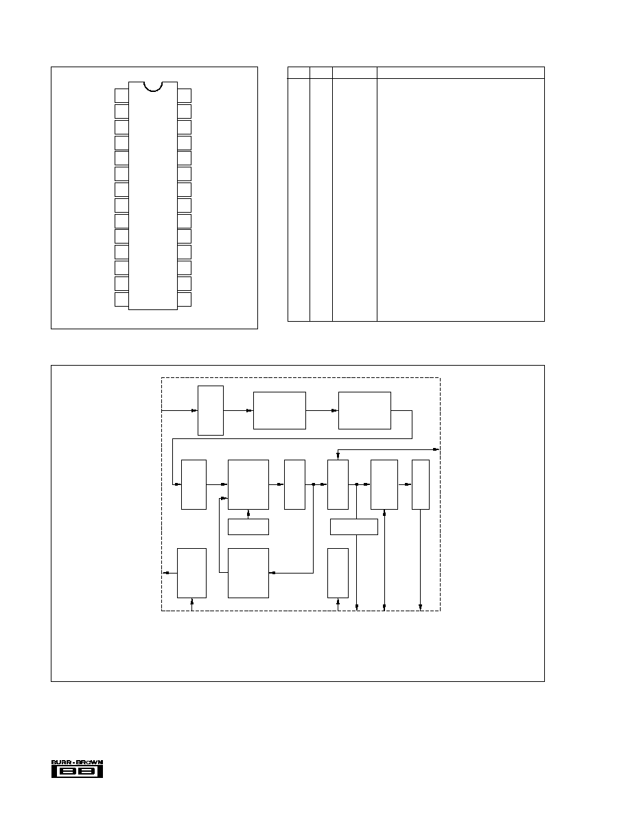
®
PCM1760P/U DF1760P/U
4
Top View
SOIC/DIP
BLOCK DIAGRAM OF DF1760
DF1760
28
27
26
25
24
23
22
21
20
19
18
17
16
15
OVL
OVR
D
3
D
2
D
1
D
0
TP1
V
SS1
V
DD1
256fs
Strobe
LRCK
CALD
CAL
V
SS2
V
DD2
TP2
CLKSEL
S/M
Mode 1
Mode 2
/PD
LRSC
FSYNC
SDATA
L/R
SCLK
SYSCLK
1
2
3
4
5
6
7
8
9
10
11
12
13
14
PIN ASSIGNMENTS DF1760
NOTE: (1) O = Output terminal; I = Input terminal.
PIN
I/O
(1)
NAME
DESCRIPTION
1
O
OVL
Left Channel Overflow Output (Active High)
2
O
OVR
Right Channel Overflow Output (Active High)
3
I
D
3
D3 Data Input (MSB)
4
I
D
2
D2 Data Input
5
I
D
1
D1 Data Input
6
I
D
0
D0 Data Input (LSB)
7
TP1
Test Pin (No Connection)
8
V
SS1
Common Channel 1
9
V
DD1
+5V Channel 1
10
O
256fs
256fs Clock Output
11
I
Strobe
Data Strobe Clock Input (128fs)
12
I
LRCK
LR Clock Input
13
I
CALD
Calibration Function Enable (Active Low)
14
O
CAL
Calibration Output (High During Calibration)
15
I
SYSCLK
System Clock Input (256fs or 384fs)
16
I
/O
SCLK
Data Clock
17
I
/O
L/R
LR Channel Phase Clock
18
O
SDATA
Serial Data Output (1fs)
19
I
/O
FSYNC
Frame Clock (2fs)
20
I
LRSC
Phase Control of LR Channel Phase Clock
21
I
/PD
Power Down Mode Enable Input (Active Low)
22
I
Mode2
Output Format Selection Input 2
23
I
Mode1
Output Format Selection Input 1
24
I
S/M
Slave/Master Mode Selection Input (High Makes
Slave Mode
25
I
CLKSEL
System Clock Selection Input (High Makes 256fs)
26
TP2
Test Pin (No Connection)
27
V
DD2
+5V Channel 2
28
V
SS2
Common Channel 2
Boost
Filter
Input
LAT
1/16
Decimation
Filter
Input
RAM
Multiplier
ALU
Calib-
ration
Output
Control
P/S
Coefficient
Overflow DET
Main
Timing
Control
Temporary
RAM
Test
SYSCLK
CLKSEL
/PD
TP1
TP2
V
SS2
V
DD2
V
SS1
V
DD1
256fs
OVL
OVR
S/M
MODE 1
MODE 2
LRSC
FSYNC
L/R
SCLK
SDATA
(16-, 20-Bit)
CALD
CAL
D
3
D
2
D
1
D
0
Strobe
LRCK
®
5
PCM1760P/U DF1760P/U
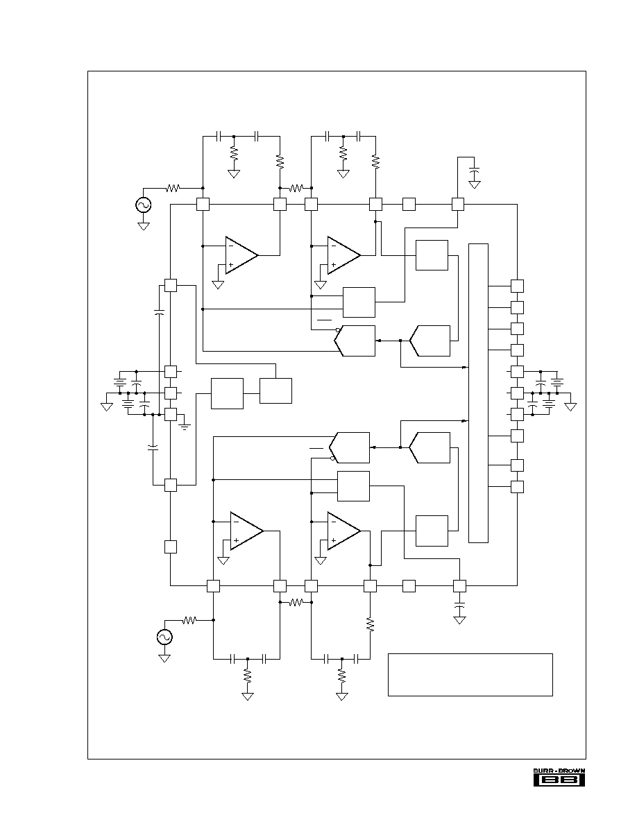
BLOCK DIAGRAM OF PCM1760
+V
CC
4
C
2
R
R
T
1R
R
IN
2R
C
1
R
R
IN
1R
C
4
R
R
Z
1R
R
T
2R
C
3
R
C
2
L
R
T
1L
R
IN
2L
C
1
L
C
4
L
R
T
2L
C
3
L
R
IN
1L
R
Z
1L
3
2
1
28
27
+
11
12
13
14
15
16
+
NC
In-1L
In-2L
Out-1L
Out-2L
NC
BPODC-L
In-1R
In-2R
Out-2R
BPODC-R
1R
2R
1L
2L
RCH
S/H
LCH
S/H
S/H
IN
L
LCH
BPO
RCH
BPO
S/H
IN
R
RCH
DAC
RCH
ADC
LCH
DAC
LCH
ADC
I
OUT
L
I
OUT
L
I
OUT
R
I
OUT
R
Band Gap
Bias
Servo
Amp
21
DGND
+
+
20
22
23
24
25
26
19
18
17
+V
DD
D
0
D
1
D
2
D
3
V
DD
256fs
Strobe
L/R CK
+5V
5V
D
e
c
o
d
e
r
T
i
m
i
n
g
C
T
L
AGND
V
CC
+
+
+5V
5V
7
8
6
Sub
SERVO
DC
5
+
+
BGDC
9
NC
10
External Components Condition
R
IN
1R/L
2.2k
C
1
, C
2
R/L
2200pF
R
TI
R/L
470
R
IN
2R/L
1.3k
C
3
, C
4
R/L
1800pF
R
T
2 R/L
560
R
Z
1 R/L
1.2k
RCH,
V
IN
Out-1R
LCH,
V
IN
®
PCM1760P/U DF1760P/U
6
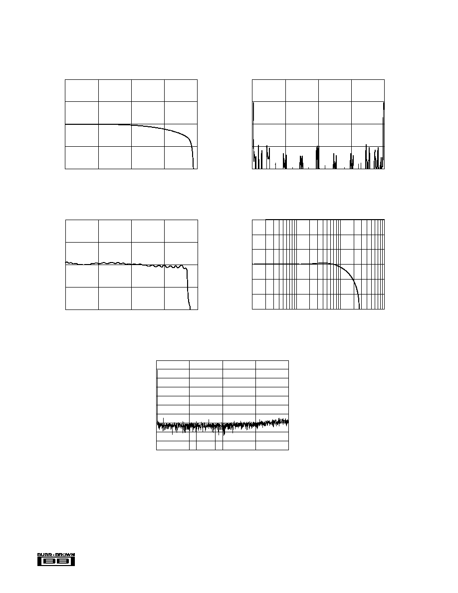
TYPICAL PERFORMANCE CURVES
OVERALL PASS-BAND
CHARACTERISTICS OF THE DF1760
1.0
0
fs
÷
2
fs
÷
4
1.0
0.5
0
0.5
(dB)
OVERALL CHARACTERISTICS OF THE DF1760
(fs)
150
0
64
16
32
46
50
0
50
100
(dB)
PASS-BAND CHARACTERISTICS
OF THE FIR PORTION OF THE DF1760
0.0010
0
fs
÷
2
fs
÷
4
0.0010
0.0005
0
0.0005
(dB)
TOTAL PASS-BAND FREQUENCY RESPONSE,
COMBINATION OF PCM1760 AND DF1760
0.3
0.3
0.2
0.1
0
0.1
0.2
Amplitude (dB)
Frequency (kHz)
0.1
1
10
100
TYPICAL FFT ANALYSIS OF THE 1kHz fs INPUT SIGNAL
200
0
24
0
20
40
60
80
100
120
140
160
180
Amplitude (dB)
6
12
18
Frequency (kHz)
fs = 48.000000kHz
F
C1
= 1.171876kHz
®
7
PCM1760P/U DF1760P/U
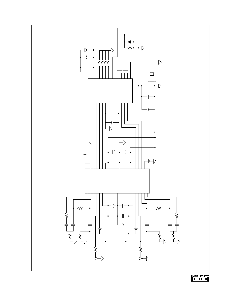
BASIC CONNECTION DIAGRAM OF PCM1760 AND DF1760
R
IN
2.2k
3.3µF
PCM1760
Out-2R
In-2R
Out-1R
In-1R
Servo DC
+V
CC
1
2
3
4
5
6
27
26
25
24
23
22
BPO DCR
D
3
D
2
D
1
D
0
+V
DD
V
CC
BG DC
In-1L
Out-1L
In-2L
Out-2L
8
9
11
12
13
14
20
19
18
17
16
V
DD
256fs
STB
L/R CLK
BPO DCL
21
DGND
AGND
7
DF1760
D
3
D
2
D
1
D
0
V
SS1
3
4
5
6
8
28
27
25
24
23
22
V
SS2
V
DD2
CLKSEL
S/M
Mode 1
Mode 2
V
DD1
256fs
STB
LRCK
9
10
11
12
19
18
17
16
15
FSYNC
SDATA
L/R
SCLK
SYSCLK
Digital I/O
3.3µF
+
0.1µF
0.1µF
+
3.3µF
0.1µF
+
3.3µF
5V
V
DD
+5V
V
DD
+5V
V
DD
+
10µF
0.1µF
+
3.3µF
+5V
V
DD
+
0.1µF
+5V V
DD
SYS CLK
0.1µF
3.3µF
0.1µF
3.3µF
+
10µF
+
10µF
+5V V
CC
5V V
CC
R
IN
2.2k
2200pF
2200pF
1.3k
470
560
1800pF
1800pF
1.2k
LCH In
RCH In
560
1800pF
1.2k
2200pF
1.3k
470
+
10µF
+
+
1800pF
2200pF
21
+
10k
47
µ
F
+5V
V
DD
Power on
Reset
PD
®
PCM1760P/U DF1760P/U
8
FUNCTIONS OF
THE DIGITAL FILTER
SYSTEM CLOCK
The DF1760 can accept a system clock of either 256fs or
384fs. If a 384fs system clock is used, the DF1760 divides
by 2/3 to create the 256fs system clock required for the
PCM1760. The system clock is applied to pin 15 (SYSCLK
input). The actual clock selection is done by setting pin 25
(CLKSEL input) "high" for 256fs clock and "LOW" for
384fs clock.
The detailed timing requirements for the system clock are
shown in Figure 3c.
CLKSEL
SYSCLK
H
256fs
L
384fs
MASTER/SLAVE MODE
The DF1760 can be used in both the master mode and slave
mode. In the master mode, the DF1760 outputs L/R (left/
right channel phase clock), SCLK (data clock) and FSYNC
(frame clock 2fs) signals. In the slave mode, the DF1760
accepts L/R, SCLK and FSYNC signals. The mode selection
is done by taking pin 24 (S/M INPUT) "HIGH" for slave
mode and "LOW" for master mode.
S/M
MODE
H
Slave
L
Master
OUTPUT DATA FORMAT
The serial output data has four possible formats. The selec-
tion of the formats can be done by the Mode 1 and Mode 2
inputs.
CALD
CALIBRATION
H
Disable
L
Enable
MODE 1
MODE 2
FORMATS
H
H
MSB First, 16 Bits, Falling Edge
L
H
MSB First, 20 Bits, Falling Edge
H
L
MSB First, 20 Bits, Rising Edge
L
L
LSB First, 20 Bits, Falling Edge
LRSC
L/R CLOCK AND CHANNEL
H
H = LCH,
L = RCH
L
L = LCH,
H = RCH
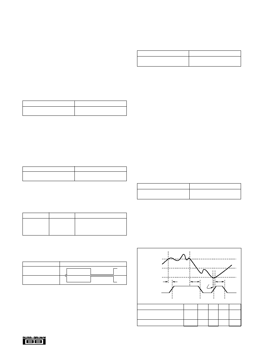
OVERFLOW DETECTION
When a near-to-clipping input condition is detected, OVL
output (Pin 1), or OVR output (Pin 2), becomes "HIGH" for
a duration of 4096/fs (about 85ms) depending upon on the
channel detected.
The OVL and OVR output return to "LOW" after
4096/fs duration automatically.
OFFSET CALIBRATION MODE
The offset error is calibrated by storing the digital data when
the input is zero in registers and subtracting it from the
future data with actual signal input.
To enable the calibration mode, set the CALD input (Pin 13)
"LOW". The calibration mode is disabled by setting the
CALD input (Pin 13) "HIGH". The calibration cycle is
initiated by setting the /PD input (Pin 21) "LOW" for more
than 2 system clock periods and then setting it "HIGH".
During the calibration cycle, the CAL output (Pin 14)
becomes "HIGH", all the serial data is forced to "LOW",
and the L/R (Pin 17), SCLK (Pin 16) and FSYNC (Pin 19)
pins become input terminals after the completion of the
calibration cycle. The CAL output is "LOW".
POWER DOWN MODE/RESET
The /PD input (Pin 21) has two functions. First, it should be
set at "HIGH" after application or restoration of power (V
SS
and/or V
DD
) to accomplish the power-on/mode reset func-
tion. The detail timing requirements for this function are
shown in Figure 3f. Second, the DF1760 is placed in the
power down mode by setting the /PD input (Pin 21) "LOW".
Set the /PD input (Pin 21) "HIGH" for normal operation
mode.
LR CHANNEL PHASE CLOCK
The status of the LR channel phase clock can be set by the
LRSC input.
/PD
OPERATION
H
Normal
L
Power Down
DESCRIPTION
NAME
MIN
TYP
MAX
UNITS
Delay from Overflow Detection
to OVL (OVR) Output
T
OR
0
ns
OVL (OVR) Output Pulse Width
T
OF
4096
1/fs
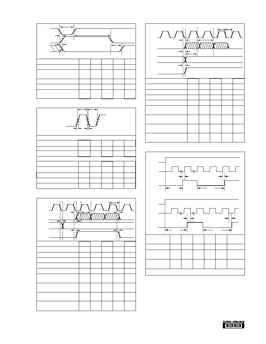
FIGURE 3a. DF1760 Overflow Detection.
T
OF
T
OR
T
OF
T
OR
OVL (OVR)
Detect Level
+Detect Level
The power dissipation of the DF1760 in the power down
mode is about 1/10 of the normal operation mode. During
the power down mode, the L/R, SCLK, and FSYNC pins
become input pins and all the serial data is forced "LOW".
The 256fs output is enabled even in the power down mode.
The detailed timing of the power down mode operation and
the offset calibration is shown in Figure 3b.
®
9
PCM1760P/U DF1760P/U
T
PCF
T
CSV
CAL
SDATA
/PD
T
PSF
T
PDW
T
PCR
DESCRIPTION
NAME
MIN
TYP
MAX
UNITS
Pulse Width of /PD Input
T
PDW
2
1/Fclk
Delay from /PD Input to
CAL Output
T
PCR
6
1/Fclk
Calibration Cycle Duration
T
PCF
4096
1/fs
Delay from /PD Input to S
DATA
L
T
PSF
6
1/Fclk
Delay from Completion of
Calibration to SDATA Valid
T
CSV
1
1/fs
FIGURE 3b. DF1760 Power Down and Offset Calibration.
SYSTEM CLOCK: 256fs
DESCRIPTION
NAME
MIN
TYP
MAX
UNITS
Low Level Duration
T
CLKL
31
ns
High Level Duration
T
CLKH
31
ns
T
CLKH
T
CLKL
2.0V
1.4V
0.8V
T
LH
T
HL
DESCRIPTION
NAME
MIN
TYP
MAX
UNITS
SCLK Frequency
F
SLK
32fs
48fs
64fs
Low Duration of FSCLK
T
SLKL
100
ns
High Duration of FSCLK
T
SLKH
100
ns
Delay from SCLK to L/R Edge
T
SLR
70
70
ns
Delay from Falling Edge of
SCLK to SDATA Valid
T
DSS
50
ns
Delay from SCLK to FSYNC
Edge
T
SF
70
0
ns
Delay from Rising Edge of
SCLK to SDATA Valid
T
DSV
100
ns
Delay from SDATA Valid to
Rising Edge of SCLK
T
SDR
100
ns
SCKL
SDATA
L/R
FSYNC
T
SLR
T
SDR
T
SF
T
DSS
T
DSV
T
SLKH
T
SLKL
FIGURE 3e. Timing of Slave Mode, DF1760.
FIGURE 3f. Power On and Mode Reset Timing.
APPLIES TO
DESCRIPTION
NAME
MIN
TYP
MAX
UNITS
(1)
MODE
Power on to PD
T
PDW
2
1/fs
Master/Slave
PD
to L/R
T
SP
1
+1
1/Fclk
Slave
(LRSC = "H")
PD
to L/R
T
SP
1
+1
1/Fclk
Slave
(LRSC = "L")
NOTE: (1) fs: sampling rate. Fclk: system clock frequency.
T
PDW
T
PDW
T
SP
T
SP
Power
L/R
PD
<LRSC = "H"
T
PDW
T
PDW
T
SP
T
SP
Power
L/R
PD
<LRSC = "L"
SYSTEM CLOCK: 384fs
DESCRIPTION
NAME
MIN
TYP
MAX
UNITS
Low Level Duration
T
CLKL
24
ns
High Level Duration
T
CLKH
24
ns
Rise Time
T
LH
6
ns
Fall Time
T
HL
6
ns
FIGURE 3c. System Clock Timing Requirements of DF1760.
T
SDR
T
SF
T
DSS
SCLK
SDATA
L/R
FSYNC
T
SLR
T
DSV
T
DSS
T
DSV
T
SF
DESCRIPTION
NAME
MIN
TYP
MAX
UNITS
SCLK Frequency
F
SLK
64fs
SCLK Frequency Duty Cycle
50
%
FSYNC Frequency
F
SYNC
2fs
FSYNC Frequency Duty Cycle
50
%
Delay from SCLK to L/R Edge
T
SLR
20
50
ns
Delay from Falling Edge of
SCLK to SDATA Valid
T
DSS
50
ns
Delay from SCLK to FSYNC
Edge
T
SF
20
50
ns
Delay from Rising Edge of
SCLK to SDATA Valid
T
SDR
100
ns
Delay from SDATA Valid to
Rising Edge of SCLK
T
DSV
100
ns
FIGURE 3d. Output Timing of Master Mode, DF1760.
®
PCM1760P/U DF1760P/U
10
The DF1760 accepts the four-bit 64fs noise shaped data
stream from the PCM1760 and decimates to 1/16 with an
initial filter, and then decimates to 1fs 20-bit data using a 4
x
oversampling filter.
The PCM1760 and DF1760 combination achieves a dy-
namic range of 108dB and SNR of 110dB even with a
single-ended input.
FIGURE 6. Multi-bit Enhanced Noise Shaping.
+
2nd Order
Integrator
4Bits
Output
ADC
DAC
4Bits
+
2nd Order
Integrator
Input
FIGURE 7. Recommended Power Supply Connection and
Decoupling.
LAYOUT PRECAUTIONS
Analog common and digital common of the PCM1760 are
not connected internally. These should be connected to-
gether with the common of the DF1760 as close to the unit
as possible, preferably to a large ground plane under the
PCM1760.
The use of a separate +5V supply is recommended for the
PCM1760 and DF1760, and to connect the common at one
point as described above. Low impedance analog and digital
commons returns are essential for better performance.
The power supplies should be bypassed with tantalum ca-
pacitors as close as possible to the units. See Figure 7 for
recommended common connections and power supplies
bypassing.
THEORY OF OPERATION
MULTI-BIT ENHANCED NOISE SHAPING
A block diagram of a typical 1-bit delta-sigma modulator is
shown in Figure 4.
In Figure 4, the quantizer consists of a single bit which has
two possible states, either "0" or "1". The input signal is
sampled at a much higher sample rate than the nyquist
sampling frequency. The quantizer output data stream is
digitally filtered for higher resolution nyquist data. The
theoretical SNR is determined by the number of the order of
the integrator and the oversampling rate.
There is a practical limit to increasing the numbers of order
of the integrator due to an inherent oscillation in the modu-
lator. There is also a limit to increasing the sample rate due
to the increase in jitter sensitivity associated with high clock
frequencies.
The PCM1760 utilizes a four-bit quantizer instead of the
conventional one-bit method. The quantizing noise of a four-
bit quantizer is 1/16 of the one-bit version. Using the four-
bit quantizer allows for a lesser order number of the integra-
tor and a lower oversampling rate to achieve similar perfor-
mance to that of a more complex one-bit system.
A block diagram of the PCM1760 modulator is shown in
Figure 6. The PCM1760 is a fourth-order integrator that
samples at 64
x
oversampling, and samples left and right
channel input signal simultaneously.
+
Integrator
Quantizer
Output
Input
z
1
FIGURE 4. Single Stage 1-Bit Delta-Sigma.
FIGURE 5. Single Stage Multi-bit Delta-Sigma.
+
Integrator
nBit
Output
Input
ADC
DAC
nBit
(1)
PCM1760
22
21
20
6
7
8
Power Supply
GND
5V
+5V
(1)
Power Supply
GND
+5V
(1)
(1)
(1)
DF1760
28
27
8
9
(2)
Digital
Common
NOTE: (1) Tantalum 3.3µF. (2) Ceramic 0.1µF.
Analog
Common
®
11
PCM1760P/U DF1760P/U
OUTPUT TONE ELIMINATION
When the sampling frequency (fs) is between 40kHz and 50 kHz
and the L/R relative offset voltage (
Vs) is less than or equal to
0.05% of full scale range, the PCM1760 may output a tone
similar to an idle tone. This tone is very low and its frequency
depends on the input L/R relative offset voltage,
Vs. This
tone never occurs when the sampling frequency (fs) is 32kHz.
To avoid this tone, the offset voltage should be summed
using an amplifier, buffer, active low pass filter, etc., to
cause the input L/R relative offset voltage (
Vs) to be
greater than 0.05% of full scale range.
It is recommended that:
(A) Sum offset at both L/R channels
Lch: V
IL
= 20mV
±
10%
Rch: V
IR
= +10mV
±
10%
(B) Sum offset at L channel
Lch: V
IL
= 30mV
±
10%
Rch: V
IR
=
±
1mV (by a precircuit)
When FSR = 5V (
±
2.5V).
Figure 8 shows an application circuit for summing the offset
at both L/R channels.
Alternately, Figure 9 shows an application circuit for use
when fs = 48kHz which changes the external integrator
circuit of the PCM1760.
MODULATOR COMPONENTS
AND SAMPLING FREQUENCY
The PCM1760/DF1760 are capable to 30kHz to 50kHz fs
sampling frequency by condition with external components
value which are shown in Basic Connection Diagram.
The characteristics of the modulator's integrator can be set
by external components. The values in the block diagram on
page five are recommended for optimized performance.
Low leakage, low voltage coefficient capacitors are recom-
mended for integration capacitors.
The tolerance of external components should be better than
±
2%.
FIGURE 8. Application Example to Eliminate the Tone
(offset voltage implementation for both chan-
nels).
OFFSET ERROR CALIBRATION
The offset voltage of the PCM1760 and the input stage of
the system can be compensated by using the calibration
mode of the DF1760. Offset calibration is shown in Figure
10. An optional analog switch is driven by a CAL output of
the DF1760. The PD input of the DF1760 is used to initiate
the calibration cycle.
ANALOG INPUT AND DIGITAL OUTPUT
Ideal output digital code range for 20-bit resolution is from
8000H (Full Scale) to 7FFFFH (+Full Scale).
The DF1760, combined with 70000H (
±
FSR) of the
PCM1760, produces a digital output code range at
±
FSR
input of 90000H (FSR).
The relationship between analog input and digital output is
shown in Table I.
C
1
C
2
CZ
1
11
12
13
14
RT
1
RZ
1
R
IN1
R
IN2
C
3
C
4
RT
2
RZ
2
PCM1760
OP1
OP2
R
IN1
= 2.2k
RT
2
= 2.2k
C
1
, C
2
, C
3
, C
4
= 1200pF
RT
1
= 470
RZ
1
= 470
CZ
1
= 220pF
R
IN2
= 1.3k
RZ
2
= 910
FIGURE 9. Application Example to Eliminate the Tone (alternative modulator's integrator circuit. Only for fs = 48kHz).
2.2k
2.2k
PCM1760
11
4
R
IN
1-L
R
IN
1-R
V
IR
= +10mV ±10%
V
IL
= 20mV ±10%
®
PCM1760P/U DF1760P/U
12
ANALOG INPUT
CONDITION
DIGITAL OUTPUT
+2.55V
+Max Input
72000H
+2.50V to +2.55V
Overflow
70000H to 72000H
(2)
+2.50V
+FSR
70000H
0V
BPZ (Ideal)
00000H
(1)
2.50V
FSR
90000H
2.83V to 2.85V
Overflow
82FFFH to 82000H
(2)
2.85V
Max Input
82000H
NOTES: (1) Incase of BPZ Error = 0. (2) Overflow detection level is over
70000H or under 82FFFH of digital output code.
TABLE I. Output Codes.
POWER SUPPLY SEQUENCING
The PCM1760 requires
±
V
CC
and
±
V
DD
power supplies. To
avoid any possibility of latch-up, the
±
V
CC
and
±
V
DD
power
should all be applied simultaneously or the +V
CC
and +V
DD
applied first followed by V
CC
and V
DD
.
FIGURE 10. Illustration of Offset Calibration.
+fs
BPZ
fs
0V
+fs
fs
ANALOG INPUT
V
OS
Digital Output
+fs
BPZ
fs
0V
+fs
fs
ANALOG INPUT
Digital Output
Analog Input
V
OS
PCM1760
DF1760
CAL
PD
V
OS
POWER-ON RESET AND MODE RESET
The timing requirements for POWER-ON RESET and
MODE RESET are shown in Figure 3f. The DF1760 re-
quires POWER-ON RESET when power is applied or re-
stored. MODE RESET is required when any of the follow-
ing has been changed: system clock, master/slave mode,
output data format, L/R clock, calibration after POWER-ON
in slave mode.
This reset should be done by holding the /PD input (pin 21)
low for more than 2/fs. Suggested reset circuits are given in
Figures 11, 12 and 13.
CLOCK INPUT
After power is applied to the DF1760, the system clock
should be provided continuously. The DF1760 employs a
dynamic logic architecture.
®
13
PCM1760P/U DF1760P/U
FIGURE 11. Master Mode Reset Circuit.
FIGURE 12. Slave Mode Reset Circuit, (LRSC = H).
FIGURE 13. Slave Mode Reset Circuit, (LRSC = L).
+
10k
10k
V
DD
V
DD
/PD
IN
/PD
IN
(1)
/PD
OUT
S/M
/PD
SDATA
L/R
SCLK
SDATA
L/R
SCLK
DF1760P/U
15
1588
47
µ
F
Power-On Reset Circuit
NOTE: (1) External /PD input: Time "L" > 2/fs.
+
10k
10k
V
DD
V
DD
V
DD
/PD
IN
/PD
IN
(1)
/PD
OUT
S/M
/PD
LRSC
SDATA
L/R
SCLK
SDATA
L/R
SCLK
DF1760P/U
15
1588
47
µ
F
Power-On Reset Circuit
NOTE: (1) External /PD input: Time "L" > 2/fs.
PR
CL
D
Q
Q
CLK
V
DD
V
DD
L/R
74HC74
+
10k
10k
V
DD
V
DD
V
DD
/PD
IN
/PD
IN
(1)
/PD
OUT
S/M
/PD
LRSC
SDATA
L/R
SCLK
SDATA
L/R
SCLK
DF1760P/U
15
1588
47
µ
F
Power-On Reset Circuit
NOTE: (1) External /PD input: Time "L" > 2/fs.
PR
CL
D
Q
Q
CLK
V
DD
L/R
74HC74
®
PCM1760P/U DF1760P/U
14
FIGURE 15b. Slave Mode and SCLK = 48fs.
TIMING CHARACTERISTICS
FIGURE 14. Input and Output Format of the DF1760 and PCM1760.
FIGURE 15a. Slave Mode and SCLK = 32fs. (Output format of the DF1760).
M
L M
L
SDATA (O)
FSYNC (I)
SCLK (I)
L/R (I)
M
L
FSYNC (I)
SCLK (I)
L/R (I)
M
L
M
M
L
M
L
M
L
M
L
L
M
M
L
· MSB First 20-Bit (1)
SDATA (O)
· MSB First 20-Bit (2)
SDATA (O)
· MSB First 16-Bit
SDATA (O)
· LSB First 20-Bit
SDATA (O)
Lch
Lch
Lch
Lch
Rch
Rch
Rch
Rch
D
3
D
2
D
1
D
0
256fs
LRCK
STROBE
®
15
PCM1760P/U DF1760P/U
FIGURE 15c. Slave Mode and SCLK = 64fs.
FIGURE 15d. Master Mode.
L/R (0)
SCLK (0)
·
MSB First 20 Bit (1)
FSYNC (0)
SDATA
(0)
·
MSB First 20 Bit (2)
FSYNC (0)
SDATA
(0)
·
MSB First 16 Bit
FSYNC (0)
SDATA
(0)
·
LSB First 20 Bit
FSYNC (0)
SDATA
(0)
L/R (1)
SCLK (1)
FSYNC (1)
·
MSB First 20-Bit (1)
SDATA
(0)
·
MSB First 20-Bit (2)
SDATA (0)
·
MSB First 16-Bit
SDATA (0)
·
LSB First 20-Bit
SDATA (0)