 | –≠–ª–µ–∫—Ç—Ä–æ–Ω–Ω—ã–π –∫–æ–º–ø–æ–Ω–µ–Ω—Ç: DSP202JP | –°–∫–∞—á–∞—Ç—å:  PDF PDF  ZIP ZIP |

DSP201
DSP202
FEATURES
q
ZERO-CHIP INTERFACE TO DSP ICs:
AD, AT&T, MOTOROLA, TI
q
SINGLE CHANNEL: DSP201
q
DUAL CHANNEL: DSP202
Two Serial Inputs or Cascade from Single
32-Bit Word
q
UPDATE RATE TO 500kHz
q
DYNAMIC SPECIFICATIONS:
Signal/(Noise + Distortion) = 90dB;
THD = ≠92dB
q
USER SELECTABLE 16-BIT OR 18-BIT
DATA WORDS
DESCRIPTION
The DSP201 and DSP202 are high performance digi-
tal-to-analog converters designed for simplicity of use
with modern digital signal processing ICs. Both are
complete with all interface logic for use directly with
DSP ICs, and provide analog output voltages updated
at up to 500kHz.
The DSP201 offers a single complete voltage output
channel, accepting either 16 bits or 18 bits of input
data, and can be driven by 16-bit, 24-bit, or 32-bit
serial ports. The DSP202 offers two complete voltage
output channels, with either two separate input ports,
or a mode to drive both output channels from a single
32-bit word.
Both the DSP201 and DSP202 are packaged in stan-
dard, low-cost 28-pin plastic DIP packages. Each is
offered in two performance grades to match applica-
tion requirements.
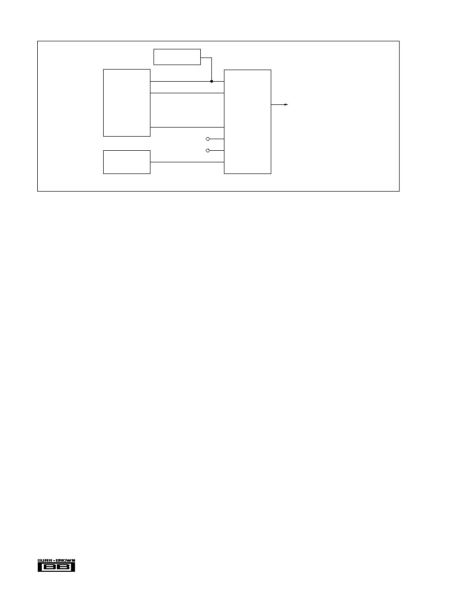
Latch Enable
Reset
Select Sync Format
Select Word Length (16/18)
Channel A Data In
Sync
Bit Clock
Channel B Data In
Cascade
Control
Logic
Convert Command
18-Bit DAC
18-Bit DAC
Reference
Channel B on DSP202 Only
Analog Voltage
Output
Channel A
Analog Voltage
Output
Channel B
Æ
International Airport Industrial Park ∑ Mailing Address: PO Box 11400 ∑ Tucson, AZ 85734 ∑ Street Address: 6730 S. Tucson Blvd. ∑ Tucson, AZ 85706
Tel: (520) 746-1111 ∑ Twx: 910-952-1111 ∑ Cable: BBRCORP ∑ Telex: 066-6491 ∑ FAX: (520) 889-1510 ∑ Immediate Product Info: (800) 548-6132
DSP-Compatible Single/Dual
DIGITAL-TO-ANALOG CONVERTERS
©
1991 Burr-Brown Corporation
PDS-1067C
Printed in U.S.A. July, 1993

Æ
DSP201/202
2
SPECIFICATIONS
ELECTRICAL
T
A
= 0
∞
C to 70
∞
C, Output Update Frequency, f
S
, = 400kHz, V
A
+ = V
D
+ = +5V, V
A
≠ = V
D
≠ = ≠5V, unless otherwise specified.
DSP201JP
DSP201KP
DSP202JP
DSP202KP
PARAMETER
CONDITIONS
MIN
TYP
MAX
MIN
TYP
MAX
UNITS
RESOLUTION
18
*
Bits
DYNAMIC RANGE
108
*
dB
ANALOG OUTPUT
Voltage Range
R
L
= 375
±
3
*
V
Impedance
0.1
*
Current
R
L
= 375
±
8
*
mA
Slew Rate
R
L
= 1.5k
, C
L
= 100pF
15
*
V/
µ
s
Settling Time to 0.006%
R
L
= 1.5k
, C
L
= 100pF
2.5
*
µ
s
for Full-Scale Step
THROUGHPUT SPEED
(1)
Update Rate
CASC = LOW on DSP202
500
*
kHz
DSP202 in Cascade Mode
CASC = HIGH
300
kHz
AC ACCURACY
(2, 3)
Signal to (Noise + Distortion) Ratio
f
OUT
= 1kHz
82
86
88
90
dB
(4)
f
OUT
= 1kHz (≠60dB)
30
32
dB
f
OUT
= 10kHz
80
86
86
90
dB
Total Harmonic Distortion
f
OUT
= 1kHz
≠90
≠85
≠92
≠88
dB
Channel Separation
f
OUT
= 1kHz to 100kHz
105
*
dB
on DSP202
DC ACCURACY
Integral Nonlinearity Error
±
0.006
±
0.004
%
Differential Nonlinearity Error
±
0.006
±
0.004
%
Bipolar Zero Error
(5)
±
10
*
mV
Bipolar Zero Error Drift
20
*
ppm FSR/
∞
C
Bipolar Zero Mismatch
(5)
DSP202 Channels
5
*
mV
Gain Error
1
3
*
*
%
Gain Error Drift
100
*
ppm/
∞
C
Gain Error Mismatch
DSP202 Channels
1
3
*
*
%
Digital Feedthrough
ENABLE = HIGH
≠105
*
dB
Power Supply Sensitivity
≠5.1 < V
A
≠, V
D
≠ < ≠4.9
≠60
*
dB
+4.9 <V
A
+, V
D
+ < +5.1
≠60
*
dB
DIGITAL INPUTS
Format
Serial; MSB first; 16/18-bit and Cascaded
Coding
Binary Twos Complement
Logic Levels
V
IL
I
IL
=
±
10
µ
A
0
+0.8
*
*
V
V
IH
I
IH
=
±
10
µ
A
+2.4
+5
*
*
V
Data Transfer Clock
Frequency
12
*
*
MHz
Duty Cycle
40
50
60
*
*
*
%
DIGITAL OUTPUTS
V
OL
I
OL
= 4mA
0
+0.4
*
*
V
V
OH
I
OH
= 4mA
+2.4
+5
*
*
V
POWER SUPPLIES
Rated Voltage
V
A
+
+4.75
+5
+5.25
*
*
*
V
V
A
≠
≠5.25
≠5
≠4.75
*
*
*
V
V
D
+
+4.75
+5
+5.25
*
*
*
V
V
D
≠
≠5.25
≠5
≠4.75
*
*
*
V
Current
I
A
+
18
*
mA
I
A
≠
17
*
mA
I
D
+
13
*
mA
I
D
≠
25
*
mA
Power Consumption
365
450
*
*
mW
TEMPERATURE RANGE
Specification
0
+70
*
*
o
C
Storage
≠40
+125
*
*
o
C
NOTES: (1) The data transfer clock must be at least 24 times the update rate for the standard mode, and 40 times the update rate in the DSP202 Cascade Mode.
(2) All dynamic specifications are based on 2048-point FFTs. (3) Data for the 1kHz test is bandlimited to 0 to 20kHz. Data for the 10kHz test is bandlimited to 0 to
40kHz. (4) All specifications in dB are referred to a full-scale output,
±
3Vp-p. (5) Adjustable to zero with external potentiometer.
Æ
DSP201/202
3
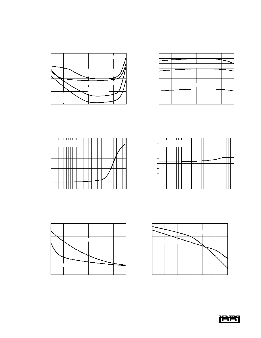
BIPOLAR ZERO ERROR AND GAIN ERROR
vs TEMPERATURE
Ambient Temperature (∞C)
Bipolar Zero Error (mV)
10
5
0
≠5
≠10
≠50
≠25
0
25
50
75
100
Gain Error (% of 6V Full Scale Range)
0.3
0.2
0.1
0
≠0.1
Gain Error
Bipolar Zero Error
INTEGRAL AND DIFFERENTIAL LINEARITY ERROR
vs TEMPERATURE (For Worst-Case Codes.)
Ambient Temperature (∞C)
Absolute Value of Error (%)
0.020
0.015
0.010
0.005
0.0
≠50
≠25
0
25
50
75
100
Differential Non-Linearity
Integral Non-Linearity
SIGNAL-TO-(NOISE + DISTORTION)
vs OUTPUT UPDATE RATE
Output Update Rate (kHz)
0.4
4
40
400
80
85
90
Signal-to-(Noise + Distortion) Ratio (dB)
f = 0dB
Output not band-limited.
OUT
TOTAL HARMONIC DISTORTION
vs OUTPUT FREQUENCY
Output Frequency (kHz)
0.2
2
20
200
≠50
≠60
≠70
≠80
≠90
≠100
Total Harmonic Distortion (dB)
f = 0dB
Output not band-limited.
OUT
SIGNAL-TO-(NOISE + DISTORTION) RATIO
vs TEMPERATURE AND AMPLITUDE
Ambient Temperature (∞C)
Signal-to-(Noise +Distortion) Ratio (dB)
100
90
80
70
60
50
40
30
20
10
0
≠50
≠25
0
25
50
75
100
f = 1kHz, 0dB
OUT
f = 1kHz, ≠60dB
OUT
f = 1kHz, ≠20dB
OUT
DYNAMIC PERFORMANCE vs TEMPERATURE
Ambient Temperature (∞C)
SINAD, SNR and SFDR (dB)
80
85
90
95
100
≠50
≠25
0
25
50
75
100
f = 1kHz, ±3Vp-p
OUT
THD (dB)
≠80
≠85
≠90
≠95
≠100
Signal-to-(Noise + Distortion)
(SINAD)
Signal-to-Noise Ratio (SNR)
Total Harmonic
Distortion (THD)
Spurious Free
Dynamic Range
(SFDR)
TYPICAL PERFORMANCE CURVES
T
A
= +25
∞
C; Update Frequency, f
S
= 400kHz; V
A
+ = V
D
+ = +5V; V
A
≠ = V
D
≠ = 5V; SWL = HIGH;
CASC = LOW; Output Bandwidth Limited to 20kHz; unless otherwise noted.
The information provided herein is believed to be reliable; however, BURR-BROWN assumes no responsibility for inaccuracies or omissions. BURR-BROWN assumes
no responsibility for the use of this information, and all use of such information shall be entirely at the user's own risk. Prices and specifications are subject to change
without notice. No patent rights or licenses to any of the circuits described herein are implied or granted to any third party. BURR-BROWN does not authorize or warrant
any BURR-BROWN product for use in life support devices and/or systems.

Æ
DSP201/202
4
INTERMODULATION DISTORTION vs TEMPERATURE
Ambient Temperature (∞C)
Intermodulation Distortion (dB)
≠85
≠90
≠95
≠100
≠105
≠50
≠25
0
25
50
75
100
f + f = 0dB
f = 9.5kHz
f = 11.5kHz
OUT 1
OUT 2
OUT 1 OUT 2
POWER SUPPLY REJECTION vs
SUPPLY RIPPLE FREQUENCY
Supply Ripple Frequency (kHz)
0.1
1
10
100
≠35
≠45
≠55
≠65
≠75
Supply Ripple Rejection (dB)
V + = V +
A D
V ≠ = V ≠
A D
OUTPUT VOLTAGE SETTLING TIME
Settling Time (µs)
0
1
2
3
4
5
6
7
8
9
10
0.1
0.01
0.001
Accuracy (% of 6V Full Scale Range)
R = 1.5k
C = 100pF
L
L
+Full Scale to
≠Full Scale Transition
≠Full Scale to
+Full Scale Transition
TYPICAL PERFORMANCE CURVES
(CONT)
T
A
= +25
∞
C; Update Frequency, f
S
= 400kHz; V
A
+ = V
D
+ = +5V; V
A
≠ = V
D
≠ = 5V; SWL = HIGH; CASC = LOW;
Output Bandwidth Limited to 20kHz; unless otherwise noted.
The DSP201 and DSP202 are ESD (electrostatic discharge)
sensitive devices, and normal standard precautions should be
taken. Permanent damage may occur on unconnected devices
subject to high energy electrostatic fields. When not in use,
devices must be stored in conductive foam or shunts. The
protective foam should be discharged to the destination socket
before devices are removed.
PACKAGE INFORMATION
PACKAGE DRAWING
MODEL
PACKAGE
NUMBER
(1)
DSP201JP
28-Pin Plastic DIP
215
DSP201KP
28-Pin Plastic DIP
215
DSP202JP
28-Pin Plastic DIP
215
DSP202KP
28-Pin Plastic DIP
215
NOTE: (1) For detailed drawing and dimension table, please see end of data
sheet, or Appendix D of Burr-Brown IC Data Book.
ORDERING INFORMATION
NUMBER
SIGNAL-TO-
OF
(NOISE + DIST.)
MODEL
CHANNELS
RATIO, dB min
1-24
25-99
100+
DSP201JP
1
82
DSP201KP
1
88
DSP202JP
2
82
DSP202KP
2
88
ABSOLUTE MAXIMUM RATINGS
V
A
+ to Analog Common ...................................................................... +7V
V
A
≠ to Analog Common ...................................................................... ≠7V
V
D
+ to Digital Common ..................................................................... +7V
V
D
≠ to Digital Common ....................................................................... ≠7V
Analog Common to Digital Common ...................................................
±
1V
Control Inputs to Digital Common ............................... ≠0.5 to V
D
+ 0.5V
Maximum Junction Temperature ..................................................... 150
o
C
Internal Power Dissipation ............................................................. 825mW
Lead Temperature (soldering, 10s) ............................................... +300
o
C
Thermal Resistance,
JA
: Plastic DIP ............................................ 50
o
C/W
ELECTROSTATIC
DISCHARGE SENSITIVITY

Æ
DSP201/202
5
DSP201 PIN ASSIGNMENTS
PIN #
NAME
DESCRIPTION
1
V
A
≠
≠5V Analog Power.
2
No Internal Connection.
3
No Internal Connection.
4
AGND
Analog Ground.
5
No Internal Connection.
6
V
D
+
+5V Digital Power.
7
V
D
+
+5V Digital Power.
8
RESET
Reset. If LOW, DAC output will be 0V after two
convert commands, and will remain there as long
as the Reset input is LOW. If HIGH, normal
operation proceeds. Two convert commands are
required after Reset goes from LOW to HIGH
before the output will relate to the input word.
9
SSF
Select Sync Format In. Tie HIGH for use with
Motorola and TI DSP ICs. Tie LOW for use with
AT&T DSP ICs.
10
SWL
Select Word Length In. If HIGH, DSP201 accepts
first 16 bits of data. If LOW, DSP201 accepts first
18 bits of data.
11
SYNC
Data Synchronization Output. Active HIGH when
SSF is HIGH, active LOW when SSF is LOW.
12
XCLK
Data Transfer Clock Input.
13
SIN
Serial Data In. MSB first, Binary Two's Comple-
ment format.
14
No Internal Connection.
15
CONV
Convert Command In. DAC is updated on falling
edge, and initiates clocking new data in.
16
DGND
Digital Ground.
17
ENABLE
Latch Enable In. If LOW, DAC output will be
latched with new data word on falling edge of
Convert Command. If HIGH, Convert Commands
will be ignored.
18
DGND
Digital Ground.
19
DGND
Digital Ground.
20
V
D
≠
≠5V Digital Power.
21
VOUT
Voltage Out.
22
AGND
Analog Ground.
23
VOS
VOS Adjust In.
24
MSB
MSB Adjust In.
25
VPOT
Trim Reference Out for MSB adjustment.
26
V
A
+
+5V Analog Power.
27
DGND
Digital Ground.
28
AGND
Analog Ground.
DSP201 PIN CONFIGURATION
1
2
3
4
5
6
7
8
9
10
11
12
13
14
28
27
26
25
24
23
22
21
20
19
18
17
16
15
V ≠
AGND
V +
V +
RESET
SSF
SWL
SYNC
XCLK
SIN
A
D
D
AGND
DGND
V +
VPOT
MSB
VOS
AGND
VOUT
V ≠
DGND
DGND
ENABLE
DGND
CONV
DSP201
A
D
Æ
DSP201/202
6
DSP202 PIN CONFIGURATION
DSP202 PIN ASSIGNMENTS
PIN #
NAME
DESCRIPTION
1
V
A
≠
≠5V Analog Power.
2
MSBB
Channel B MSB Adjust In.
3
VOSB
Channel B VOS Adjust In.
4
AGNDB
Channel B Analog Ground.
5
VOUTB
Channel B Voltage Out.
6
V
D
+
+5V Digital Power.
7
V
D
+
+5V Digital Power.
8
RESET
Reset. If LOW, DAC output will be 0V after two
Convert Commands, and will remain there as long
as the Reset input is LOW. If HIGH, normal
operation proceeds. Two Convert Commands are
required after Reset goes from LOW to HIGH
before the output will relate to the input word.
9
SSF
Select Sync Format In. Tie HIGH for use with
Motorola and TI DSP ICs. Tie LOW for use with
AT&T DSP ICs.
10
SWL
Select Word Length In. If HIGH, DSP202 accepts
first 16 bits of data. If LOW, DSP202 accepts first
18 bits of data. Must be HIGH if CASC is HIGH.
11
SYNC
Data Synchronization Output. Active HIGH when
SSF is HIGH, active LOW when SSF is LOW.
12
XCLK
Data Transfer Clock Input.
13
SINA
Channel A Serial Data In. MSB first, Binary Two's
Complement format. In Cascade Mode, connect to
SINB and to DSP IC output.
14
SINB
Channel B Serial Data In. MSB first, Binary Two's
Complement format. In Cascade Mode, connect to
SINA and to DSP IC output.
15
CONV
Convert Command In. DAC is updated on falling
edge, and initiates clocking new data in.
16
CASC
Select Cascade Mode In. If HIGH, DSP202
accepts a 32-bit word, and uses the first 16 bits to
update channel A, and the second 16 bits to
update channel B. In Cascade Mode, SINA and
SINB are connected together. If CASC is LOW,
data is strobed into both channels on each clock
cycle.
17
ENABLE
Latch Enable In. If LOW, DAC output will be
latched with new data word on falling edge of
Convert Command. If HIGH, Convert Commands
will be ignored.
18
DGND
Digital Ground.
19
DGND
Digital Ground.
20
V
D
≠
≠5V Digital Power.
21
VOUTA
Channel A Voltage Out.
22
AGNDA
Channel A Analog Ground.
23
VOSA
Channel A VOS Adjust In.
24
MSBA
Channel A MSB Adjust In.
25
VPOT
Trim Reference Out for MSB adjustments.
26
V
A
+
+5V Analog Power.
27
DGND
Digital Ground.
28
AGND
Analog Ground.
1
2
3
4
5
6
7
8
9
10
11
12
13
14
28
27
26
25
24
23
22
21
20
19
18
17
16
15
V ≠
MSBB
VOSB
AGNDB
VOUTB
V +
V +
RESET
SSF
SWL
SYNC
XCLK
SINA
SINB
A
D
D
AGND
DGND
V +
VPOT
MSBA
VOSA
AGNDA
VOUTA
V ≠
DGND
DGND
ENABLE
CASC
CONV
DSP202
A
D

Æ
DSP201/202
7
THEORY OF OPERATION
The DSP201 and DSP202 are basic voltage output digital-
to-analog converters with complete logic interface circuitry
for ease of use with standard digital signal processing ICs.
Data words are transmitted from the DSP IC on its serial
port, leaving the DSP IC parallel ports free for digital
communication.
The DSP201 and DSP202 are pipelined internally. When the
user gives a convert command at time t, two actions are
initiated. First, the data stored in the internal shift registers
following the previous convert command (at t ≠ 1) is used to
update the output D/A converters immediately. Second, the
DSP201 or DSP202 transmits a synchronization pulse to the
DSP IC and starts clocking new data into the shift register
using the system Bit Clock. This data is then used to update
the D/As when the t + 1 convert command is received.
Both the DSP201 and DSP202 are 18-bit D/As internally.
On-chip logic can be programmed to use 18-bits of data to
update the D/A outputs, or can be programmed to update the
D/A based on 16-bit data words. Additionally, the logic in
the DSP202 can accept a 32-bit data word (the Cascade
Mode), and update both D/A channels simultaneously with
16 bits each. All of these modes can be hard-wired or logic-
controlled externally, so that no extra overhead on the part
of the DSP IC is required.
In the 16-bit modes, the DSP201 and DSP202 will append
zeros to the 16-bits transferred to each of the internal D/As,
which are full 18-bit converters. The 18-bit word-length
mode can be used with DSP ICs programmed for either 24-
bit or 32-bit output words, in which case the DSP201 or
DSP202 will clock in the first 18-bits of data after the
synchronization pulse, and ignore additional information on
the serial line. When programmed to accept 16-bit words,
the DSP201 and DSP202 can be used with DSP ICs pro-
grammed to output 16-, 24-, or 32-bit words, and will ignore
additional information after the first 16 bits on the serial line.
The DSP201 and DSP202 are complete voltage output D/A
converters, with on-chip references and output amplifiers to
drive
±
3V into 375
loads. State-of-the-art bipolar tech-
nologies are used in the D/A section to maximize the output
update rate, to maximize dynamic performance, and to
eliminate glitch problems. Advanced plastic packaging meth-
ods makes this performance attainable economically.
BASIC OPERATION
DATA FORMAT AND OUTPUT LEVELS
The DSP201 and DSP202 accept serial data, MSB first, in
standard Binary Two's Complement format. The length of
the data words can be selected as shown below, and the
D/A output level generated by a specific input code is shown
in Table I.
As with all standard D/As, the output ranges from negative
full scale (≠3V) to 1 LSB below positive full scale (+3V ≠
1LSB). The bipolar output amplifiers are designed to drive
375
loads at full speed and accuracy.
UPDATING THE OUTPUT
With ENABLE (pin 17) LOW, the falling edge of a Convert
Command arriving on CONV (pin 15) will immediately
update the D/A outputs with the data stored in the internal
shift registers following the previous Convert Command.
The Convert Command can be asynchronous to any other
signals or clocks without reducing accuracy, although sys-
tem accuracy is often enhanced by synchronizing digital
signals.
For a full-scale change in the input code, the output will
typically settle to within
±
0.006% of its final level within
2.5
µ
s. The slew rate of the output amplifier is typically 15V/
µ
s, for a full power bandwidth close to 800kHz. All of the
specifications and typical performance curves are achieved
with a full 400kHz update rate, unless otherwise specified.
The DSP201 and DSP202 are guaranteed operational to a
full 500kHz update rate, which exceeds the maximum Bit
Clock rate for most standard DSP ICs.
DATA TRANSFER
Data is transmitted serially to the DSP201 or DSP202, and
is clocked into the internal shift registers on the rising edge
of the external Data Transfer Clock or Bit Clock (XCLK
input on pin 12.) This clock can be as fast as 12MHz. The
Data Transfer Clock can tolerate duty cycles from 40% to
60%.
As indicated in the timing diagrams in Figure 1, either 16-
or 18-bits of data will be clocked into the DSP201 or
DSP202, or 32-bits will be clocked into the DSP202 in the
INPUT CODE
OUTPUT VOLTAGE
16-BIT MODE AND
HEX
16-BIT MODE AND
BINARY
DSP202 CASCADE MODE
18-BIT MODE
DSP202 CASCADE MODE
18-BIT MODE
0111...1111
7FFF
1FFFF
+2.999908V
2.999977V
0000...0000
0000
00000
0V
0V
1111...1111
FFFF
3FFFF
≠92
µ
V
≠23
µ
V
1000...0000
8000
20000
≠3.000000V
≠3.000000V
Theoretical LSB Size
91.6
µ
V
22.9
µ
V
TABLE I. Output Voltage vs Input Code.

Æ
DSP201/202
8
FIGURE 1. DSP201 and DSP202 Timing.
XCLK
CONV
SYNC (SSF = HIGH)
SYNC (SSF = LOW)
ENABLE
SINA/B (CASC = LOW on DSP202)
XCLK
CONV
SINA/B (CASC = HIGH)
Bit 1 (MSB)
t
2
t
5
t
3
t
2
t
6
t
7
t
6
t
7
t
9
t
8
t
10
t
11
Bit 1 (MSB)
Bit 2
Bit 16
Bit 17
Bit 18 (LSB)
t
4
t
10
t
11
Bit 1 (MSB)
Bit 2
Bit 16 (LSB)
t
2
t
1
t
1
t
2
Bit 16 (LSB)
(3)
(3)
(1)
DSP202 Cascade Mode (CASC = HIGH)
Channel A Data
Channel B Data
RESET
t
8
(2)
INTERVAL
DESCRIPTION
MIN
MAX
UNITS
t
1
XCLK period; Duty Cycle 50%
±
10%
83
ns
t
2
Convert Command LOW Time
50
ns
t
3
Convert Period (CASC = LOW on DSP202)
24
t
1
t
4
Convert Period (CASC = HIGH on DSP202
40
t
1
t
5
SYNC Active Delay after Convert Falling Edge)
t
1
+40
2 t
1
ns
t
6
SYNC LOW to HIGH Delay from XCLK Rising; C
L
= 50pF
15
ns
t
7
SYNC HIGH to LOW Delay from XCLK Rising; C
L
= 50pF
15
ns
t
8
ENABLE Setup before Convert Falling Edge
(1)
50
ns
t
9
ENABLE Hold after Convert Falling Edge
(1)
50
ns
t
8
RESET Setup before Convert Falling Edge
50
ns
t
10
SINA/B Data Setup before XCLK Rising
20
ns
t
11
SINA/B Data Hold after XCLK Rising
0
n
s
NOTES: (1) Normally tied LOW so that previously transmitted data is used to update DAC output on falling edge of
CONV. ENABLE HIGH prevents the DAC from being updated. (2) RESET must be held LOW for two complete
Convert Command cycles, and ENABLE must be LOW. (3) Optional data bits. Clocked into DAC register only if SWL
is LOW.

Æ
DSP201/202
9
Cascade Mode, but internal digital overhead requires addi-
tional Data Transfer Clock cycles before a new Convert
Command can be sent. The minimum time between Convert
Commands is 24 times the Data Transfer Clock period for
either the DSP201 or the DSP202 in standard modes, and 40
times the Data Transfer clock period for the DSP202 in the
Cascade Mode. There is no maximum time between Convert
Commands.
These additional clock cycles are used to set up the internal
shift registers and logic, and are included in the specifica-
tions for maximum update rate. This means a 12MHz Bit
Clock can achieve the maximum specified update rate of
500kHz.
DATA SYNCHRONIZATION
The DSP201 and DSP202 have internal logic to generate a
synchronization pulse (SYNC on pin 11) to signal the host
processor to transmit data. The synchronization pulse is sent
when a Convert Command is received, and the SYNC output
changes on the rising edge of XCLK. Timing is shown in
Figure 1.
The synchronization pulse can be programmed to be either
active High or active Low, depending on the logic level
input on SSF (Select Sync Format on pin 9.) If SSF is LOW,
SYNC will be normally HIGH, and will transmit a LOW
pulse after a Convert Command is received. If SSF is HIGH,
SYNC will be normally LOW, and will transmit a HIGH
pulse after a Convert Command is received. The SYNC
pulse will be as wide as one clock cycle on the Data Transfer
Clock input on XCLK (pin 12.)
SELECTING WORD LENGTH
If the Select Word Length input (SWL, pin 10) is HIGH, the
DSP201 or DSP202 will accept 16 bits of data after a Convert
Command, with the timing shown in Figure 1. After these 16
bits, additional data on SIN (DSP201 pin 13) or SINA and
SINB (DSP202 pins 13 and 14) will be ignored. Transparent
to the user, the internal shift register will append two zeroes
to the 16-bit data words before updating the D/As on the next
Convert Command.
If SWL is LOW, the DSP201 or DSP202 will clock 18 bits
of data into the internal shift register after a Convert Com-
mand, with the timing shown in Figure 1. Subsequent data
on SIN (DSP201 pin 13) or SINA and SINB (DSP202 pins
13 and 14) will be ignored.
In the 16-bit mode, an increment of 1 LSB will change the
D/A output by approximately 91.6
µ
V (the 6V full scale
range divided by 2
16
), while an LSB in the 18-bit mode will
change the output approximately 22.9
µ
V (6V/2
18
).
The DSP201 and DSP202 analog performance is tested in
production using the 16-bit mode (with SWL HIGH), and
the typical performance curves were generated using the 16-
bit mode. Verification is made during final test that the 18-
bit mode functions, but the extra resolution of these last two
bits is not used when testing the analog performance.
DSP202 CASCADE MODE
If CASC on the DSP202 (pin 16) is HIGH, the Cascade
Mode is implemented. In this mode, SINA (pin 13) and
SINB (pin 14) are strapped together and connected to the
serial output port of an appropriate DSP IC or other data
word source. A Convert Command initiates the transfer of a
32-bit word to the DSP202.
In the Cascade Mode, care must be taken to make sure SWL
(pin 10) is HIGH.
LATCH ENABLE
If ENABLE (pin 17) is LOW, the D/A outputs will be
latched with new data on the falling edge of the Convert
Command. Taking ENABLE HIGH causes the DSP201 or
DSP202 to ignore Convert Commands. With ENABLE
HIGH when a Convert Command arrives at time t, data
latched in the internal shift register after the Convert Com-
mand at t ≠ 1 is not latched to the D/As, but a new
synchronization pulse is still generated and the data in the
shift register is overwritten. This feature allows multiple
DSP201s or DSP202s to share a single DSP IC and still be
independently updated.
RESET
Taking RESET (pin 8) LOW will cause the D/As to output
0V after two Convert Commands are received. The two
Convert Commands clear out the internal shift registers, and
data input on the serial input lines will be ignored while
RESET is low. This facilitates designing an analog output
system that goes into a known, benign state either at power-
up, after fault conditions or during a calibration cycle.
ENABLE (pin 17) must be LOW when resetting the DSP201
or DSP202 outputs to 0V.
After RESET is taken HIGH, two Convert Commands are
required before the output will relate to the input data. Also,
ENABLE must be LOW for the data to be latched to the D/As.
The first Convert Command again latches the outputs at 0V,
and the second Convert Command drives the output to the
level determined by the data clocked in after the first Convert
Command.
A RESET command after power up is not required for proper
operation of the DSP201 or DSP202.
LAYOUT CONSIDERATIONS
Because of the high resolution, linearity and speed of the
DSP201 and DSP202, system design problems such as
ground path resistance, contact resistance and power supply
quality become very important.
GROUNDS
To achieve the maximum performance from the DSP201 or
DSP202, care should be taken to minimize the effect of
current flows in the system grounds that may corrupt the
output voltages generated by the D/As. Pin 22 on the
DSP201 and pins 4 and 22 on the DSP202 are the most

Æ
DSP201/202
10
critical internal grounds, and care should be taken especially
at these points to make them as close as possible to the same
potential as the system analog ground. The design of the
DSP201 and DSP202 insures that these pins will have
minimal current flowing through them.
Internally, power currents are directed to the digital grounds
(pins 18, 19, and 27) for internal digital currents, which are
primarily switching currents, and to the analog grounds (pin
28, plus pin 4 on the DSP201) for analog currents, which are
primarily from the internal current switches and the output
amplifier. Pin 16 on the DSP201 is used internally as a logic
level, and injects essentially no current into the ground.
Wherever possible, it is strongly recommended that separate
analog and digital ground planes be used. With an LSB level
of 92
µ
V in 16-bit modes, and one quarter of that in 18-bit
modes, the currents switched in a typical DSP system
(processor, memory, etc.) can easily corrupt the output
accuracy of the D/A's unless great care is taken to analyze
and design for current flows.
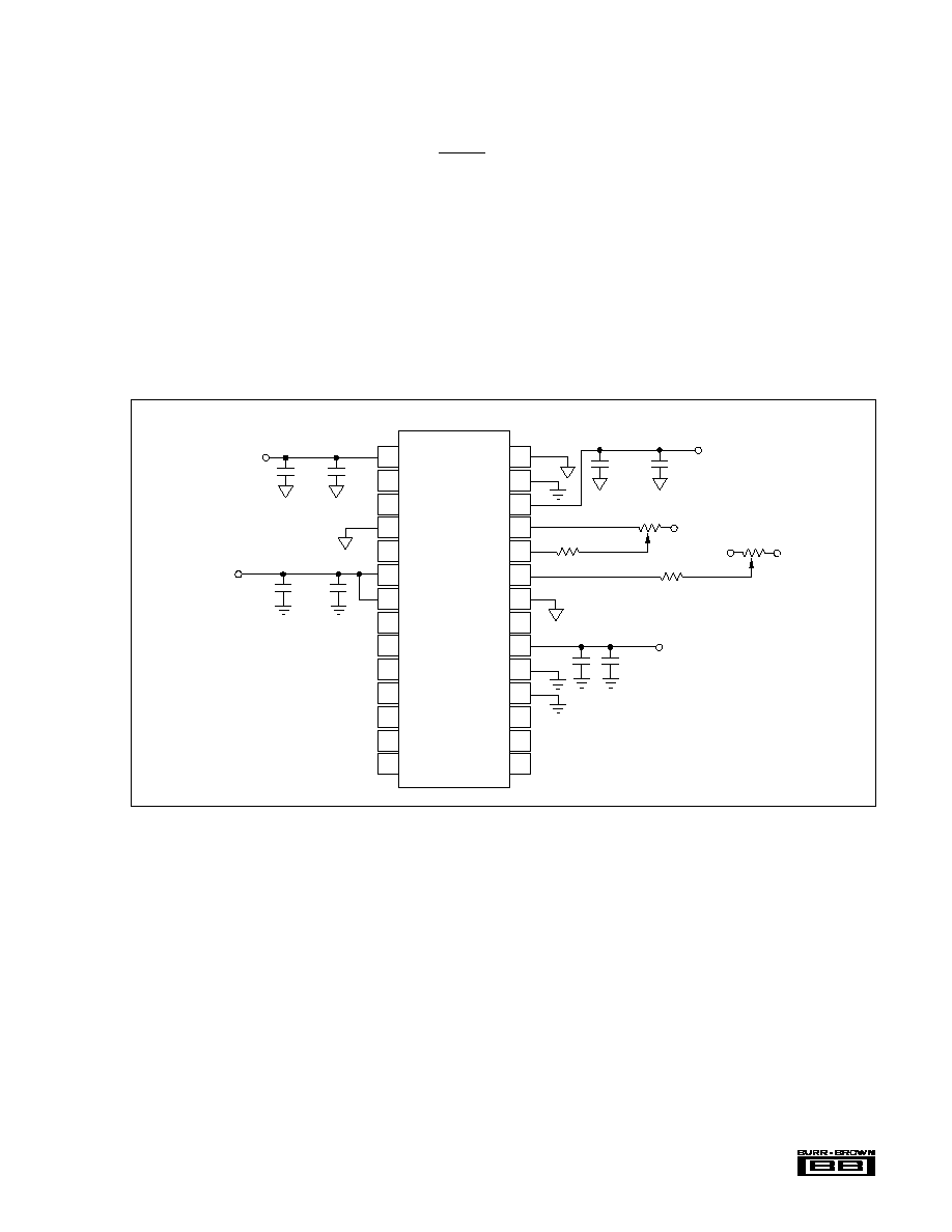
POWER SUPPLY DECOUPLING
All of the supplies should be decoupled to the appropriate
grounds using tantalum capacitors in parallel with ceramic
capacitors, as shown in Figures 2 and 3. For optimum
performance of any high resolution D/A, all of the supplies
need to be as clean as possible. If separate digital and analog
supplies are available in a system, care should be taken to
insure that the difference between the analog and the digital
supplies is not more than 0.5V for more than a few hundred
milliseconds, as may occur at power-on.
Separate ≠5V analog and digital supplies are not needed.
These pins are kept separate internally to minimize cou-
pling. Drive pin 20 from the ≠5V analog supply, and make
sure that the decoupling shown in Figure 2 or 3 are placed
as close as possible to the D/As.
CALIBRATION AND ADJUSTMENT
OPTIONAL EXTERNAL OFFSET AND MSB TRIMS
All of the specifications for the DSP201 and DSP202, plus
the typical performance curves, are based on the perfor-
mance of these D/As without external trims. In most appli-
cations, external trims are not required.
If external trims are not used, pins 23, 24, and 25 on the
DSP201 should be left open, as should pins 2, 3, 23, 24 and
25 on the DSP202. These pins should not be decoupled with
capacitors or tied to any specific potential, or the noise on
the D/A outputs may increase.
ADJUSTING OFFSET
Where required by specific applications, offsets can be
trimmed using the circuits in Figure 2 (DSP201) or Figure 3
(DSP202.) As with all standard D/As, offset on the DSP201
and DSP202 means the difference of the output from the
ideal negative full scale value. The DSP201 and DSP202 use
a current switching D/A architecture, and the current from
this is internally amplified to produce a
±
3V output range.
Negative full scale output thus results from having all of the
internal current switches turned off. Offset on the DSP201
and DSP202 should not be confused with the delta from 0V
with an input code of 0000...0000 (0000 hex for 16-bit
Modes, 00000 hex for 18-bit Modes). This is often described
as bipolar zero error, and includes the effects of both offset
and gain error.
To trim the offsets, first latch the D/As with 1000...0000
(8000 hex or 20000 hex). Then adjust the offset adjustment
pots to produce an output of ≠3.000000V.
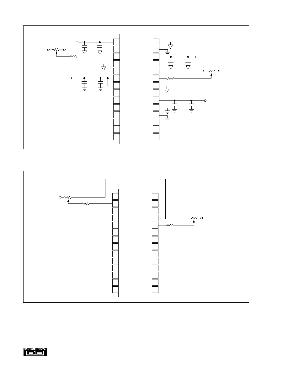
ADJUSTING THE MSB WEIGHT
The MSB adjustment circuitry shown in Figure 2 for the
DSP201 and in Figure 4 for the DSP202 basically change the
weight of the MSB by adding to or subtracting from the
current controlled by the internal MSB switch.
Depending on the application, the MSB adjustments can be
made in one of three different ways to optimize the system
performance using the DSP201 or DSP202. For dynamic
performance, the MSB can be adjusted to minimize distor-
tion of either a full-scale or low level sine-wave output. For
applications stressing differential linearity, the 0000...0000
(0000 hex or 00000 hex) to 1000...0000 (FFFF hex or 3FFFF
hex) transition can be trimmed to change the output of the
D/As precisely 1 LSB (92
µ
V in the 16-bit Mode or 23
µ
V
in the 18-bit Mode.)
To adjust for minimum distortion of full-scale sinewaves,
strobe the inputs to the DSP201 or DSP202 with codes
representing ideal full scale sine waves, then trim the MSB
adjustment circuit to minimize distortion, as measured by
either a distortion analyzer or by digitizing the output with
an appropriate A/D and running FFT analyses.
In many audio applications, it is more appropriate to adjust
for minimum distortion with low level sinewave outputs.
This minimizes zero-crossover error, which can be a con-
cern in high-end audio systems. To do this, strobe the inputs
to the DSP201 or DSP202 with codes representing ideal
low-level sine waves (≠60dB from full scale works well),
and then trim the MSB adjustment circuit to minimize
distortion, again using a distortion analyzer or FFT analyses
to check the results of the trims.
The MSB adjustment circuits can also be used to trim the
D/A outputs directly for the transition from 0000...0000 (0000
hex or 00000 hex) to 1111...1111 (FFFF hex or 3FFFF hex),
eliminating differential linearity error at the major carry.
Ideally, this transition of the digital input code should cause
the D/A outputs to change 92
µ
V in the 16-bit Mode or 23
µ
V
in the 18-bit Mode. A simple way to make this adjustment
is to continually load alternately the codes 1111...1111 (FFFF
hex or 3FFFF hex) and 0000...0000 (0000 hex or 00000 hex)
into the DSP201 or DSP202. An amplifier with sufficient gain
can then drive an oscilloscope input, and the transition output
step can be adjusted.
Æ
DSP201/202
11
GAIN ERROR
Gain error on the DSP201 or DSP202 cannot be directly
adjusted. If required in a specific application, gain can be
trimmed out at the system level by adjusting the gain used
in an output amplifier stage, such as would be used in any
active output filter. In this case, the bipolar zero error should
be adjusted first as discussed above. Then, the gain on the
output amplifier should be adjusted to minimize the devia-
tion from ideal for ≠Full Scale (1000...000; 8000 hex or
20000 hex) and +Full Scale (0111...1111; 7FFF hex or
1FFFF hex.)
An alternative for calibrating on a bench is to tie SIN (DSP201
pin 13) or SINA and SINB (DSP202 pins 13 and 14) HIGH,
and provide a Bit Clock and periodic Convert Commands.
This loads 1111...1111 (FFFF
HEX
or 3FFFF
HEX
), driving the
output to 1LSB below 0V. Then periodically bring RESET
(pin 8) LOW for at least two Convert Commands, which is
the equivalent of loading all 0s, so the output is 0V. Now
the output can be adjusted for an ideal transition step.
ADJUSTING BIPOLAR ZERO ERROR
If it is important in a specific application to adjust bipolar
zero error, the user should first adjust the MSB trim circuits,
and then use the offset adjust circuits to adjust the outputs to
0V with input codes of all 0s (0000...0000; 0000 hex or
00000 hex.) In this case, it is not possible to also trim offset
at ≠Full Scale, as described above.
FIGURE 2. DSP201 Power Supply Connections and Optional Adjust Circuits.
1
2
3
4
5
6
7
8
9
10
11
12
13
14
28
27
26
25
24
23
22
21
20
19
18
17
16
15
DSP201
≠5V
100k
100k
2.2µF
AGND
V +
VPOT
MSB
VOS
AGND
V ≠
DGND
DGND
2.2µF
V ≠
AGNDB
V +
V +
≠5V
+5V
2.2µF
A
A
D
D
D
2.2µF
+5V
≠5V
+5V
100k
3.3k
Offset Adjust
≠5V
0.01µF
+
0.01µF
+
0.01µF
+
0.01µF
+
MSB Adjust
Æ
DSP201/202
12
FIGURE 4. DSP202 Optional MSB Adjust Circuit.
1
2
3
4
5
6
7
8
9
10
11
12
13
14
28
27
26
25
24
23
22
21
20
19
18
17
16
15
DSP202
≠5V
100k
≠5V
100k
100k
100k
Channel B
VPOT
Channel A
MSBA
MSBB
MSB Adjust
MSB Adjust
FIGURE 3. DSP202 Power Supply Connections and Optional Offset Voltage Adjustment.
1
2
3
4
5
6
7
8
9
10
11
12
13
14
28
27
26
25
24
23
22
21
20
19
18
17
16
15
DSP202
≠5V
100k
+5V
100k
3.3k
3.3k
Channel B
Offset Adjust
2.2µF
AGND
V +
VOSA
AGNDA
V ≠
DGND
DGND
Channel A
Offset Adjust
0.01µF
V ≠
VOSB
AGNDB
V +
V +
≠5V
≠5V
+5V
0.01µF
A
A
D
D
D
+5V
2.2µF
+5V
≠5V
0.01µF
+
+
2.2µF
2.2µF
+
0.01µF
+
Æ
DSP201/202
13
APPLICATIONS
USING PARALLEL PORTS
WITH THE DSP201 OR DSP202
Figure 5 shows a circuit for converting parallel outputs into
the serial data stream required by the DSP201, and meets the
requirements for timing signals. Doubling this circuit allows
the DSP202 to be driven from a 32-bit parallel port. In most
applications, this circuit can be easily incorporated into gate
arrays or other programmed logic circuits already used in the
system, since the extra gate count is not high.
DEGLITCHING
Particularly in high resolution D/A converters, changing
input codes may cause glitching on the output that exces-
sively corrupts the dynamic purity of an output signal. The
DSP201 and DSP202 are designed to minimize output
glitching, and all of the performance specifications and
typical performance curves are based on tests with no extra
deglitching circuitry. In particular, the guaranteed Signal-to-
(Noise + Distortion) performance would be impossible to
attain with any significant glitching.
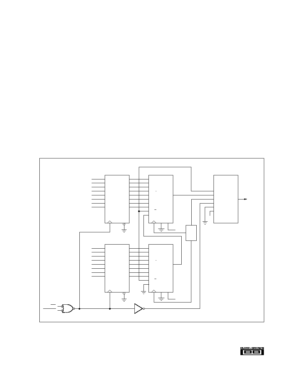
COMPLETE ANALOG INPUT/OUTPUT SYSTEM
The DSP201 or DSP202 can be paired with the Burr-Brown
DSP101 or DSP102 analog-to-digital converter to provide
both analog input and analog output for a complete digital
signal processing system. The DSP101 and DSP102 are
respectively single and dual channel 200kHz sampling A/Ds
with easy to use interfacing logic that complement the
DSP201 and DSP202. Figure 6 shows a single channel
analog input and output system based on a DSP201 and a
DSP101, and the minimal connections required to interface
to a DSP IC. A pair of channels can be implemented using
a single DSP202 and a single DSP102, either with two
separate DSP ICs, with a single DSP IC with dual serial
input and output channels, or a single DSP IC capable of 32-
bit words in the Cascade Mode.
For maximum flexibility in system design, the DSP201 or
DSP202 D/As can be updated at a different rate than the
conversion rate used on the DSP101 or DSP102 A/Ds, and
either or both of these rates can be asynchronous to the
clocks used with the DSP IC.
FIGURE 5. Driving the DSP201 from a 16-Bit Parallel Port.
8D
7D
6D
5D
4D
3D
2D
1D
18
17
14
13
8
7
4
3
74LS32
74LS04
2
1
6
WR
PORTAO
4
5
19
16
15
12
9
6
5
2
8Q
7Q
6Q
5Q
4Q
3Q
2Q
1Q
CK
OE
H
G
F
E
D
C
B
A
S/L
SI
14
12
11
10
5
4
3
2
15
1
13
QH
C
CI
CL
74LS374
74LS166
11
1
7
6
9
+5V
TTL
Bit
Clock
SYNC
SIN
XCLK
CONV
SSF
SWL
11
13
12
15
9
10
21
VOUT
DSP201
±3V
Analog
Output
8D
7D
6D
5D
4D
3D
2D
1D
18
17
14
13
8
7
4
3
19
16
15
12
9
6
5
2
8Q
7Q
6Q
5Q
4Q
3Q
2Q
1Q
CK
OE
H
G
F
E
D
C
B
A
S/L
SI
14
12
11
10
5
4
3
2
15
1
13
QH
C
CI
CL
74LS374
74LS166
11
1
7
6
9
+5V
D0
D1
D2
D3
D4
D5
D6
D7
D8
D9
D10
D11
D12
D13
D14
D15
LSB
MSB
+5V
Æ
DSP201/202
14
FIGURE 6. Analog Input and Analog Output System.
*See Burr-Brown DSP101/102 product data sheet for full description of this ADC.
DSP PROCESSOR
SYNC FORMAT
SERIAL I/O WORD
*SSF
**SWL
DSP32C, DSP16
Active Low
16 Bits
LOW
HIGH
DSP56001
Active High
24 Bits
HIGH
LOW
DSP56001
Active High
16 Bits
HIGH
HIGH
TMS320C25/C30
Active High
16 Bits
HIGH
HIGH
ADSP2101/2105
Active High
16 Bits
HIGH
HIGH
TTL Bit
Clock
12
13
11
9
10
15
XCLK
SIN
SYNC
SSF
SWL
CONV
±3V Analog Output
21
VOUT
DSP201
Conversion Rate
Generator
XCLK
SOUT
SYNC
SSF
CONV
DSP101*
*SSF
**SWL
16
20
15
12
21
2 VIN
±2.75V
Analog Input
CLKR
DATA IN
SYNC
XCLK
DATA OUT
SYNC
*SSF
Digital Signal
Processor IC
DIGITAL SIGNAL PROCESSOR
SYNC FORMAT
DATA LENGTH
DSP32C
Logic 0
16-Bit, Logic 1
DSP16
Logic 1
16-Bit, Logic 1
DSP56001 in 16-bit Mode
Logic 1
16-Bit, Logic 1
DSP56001 in 24-bit Mode
24-Bit, Logic 0
TMS320C25
Logic 1
16-Bit, Logic 1
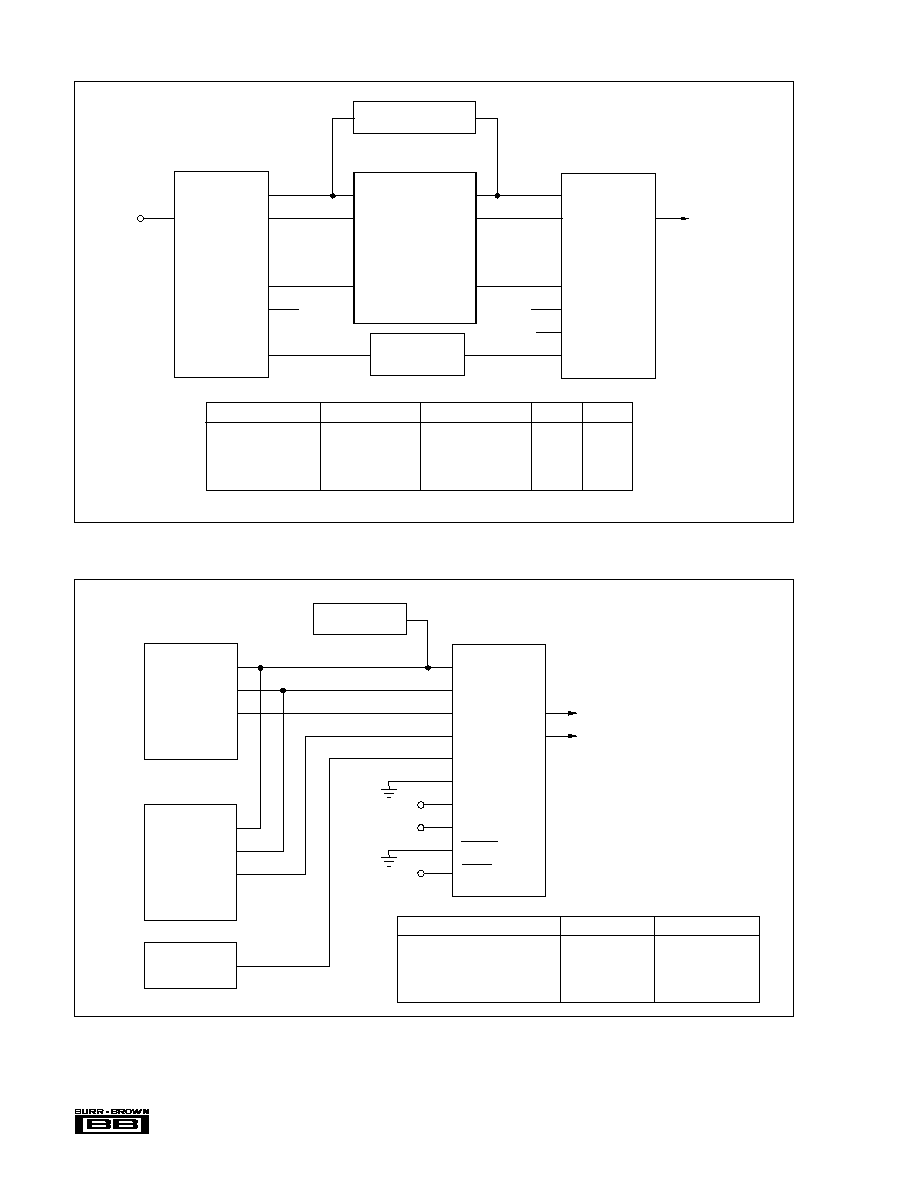
FIGURE 7. DSP202 with Dual DSP ICs.
TTL Bit
Clock
12
11
13
14
15
16
9
10
17
8
XCLK
SYNC
SINA
SINB
CONV
CASC
SSF
SWL
ENABLE
RESET
Data Length
±3V Analog Output from DSP #1
21
VOUTA
VOUTB
DSP202
Conversion Rate
Generator
TXCLK
SYNC
DATA
DSP #1
+5V
±3V Analog Output from DSP #2
5
Sync Format Input
TXCLK
SYNC
DATA
DSP #2

Æ
DSP201/202
15
USING DSP201 AND DSP202
WITH TEXAS INSTRUMENTS DSP ICS
Figures 6 thru 12 show various ways to use the DSP201 and
DSP202 with DSP ICs from the Texas Instruments
TMS320Cxx series. For simplicity, all of these circuits are
based on using the TMS320Cxx in the mode where SSF
(Select Synch Format, pin 9) is tied HIGH, so that there is
an active High synchronization pulse generated by the
DSP201 or DSP202 after receiving a Convert Command.
The synchronization pulse can be changed to active Low
simply by making SSF LOW, where appropriate, without
changing basic operation of the D/As. The timing for either
synchronization mode is shown in Figure 1.
In all cases, the DSP201 and DSP202 expect to receive the
data with the MSB first, and the TMS320Cxx needs to be
programmed for this.
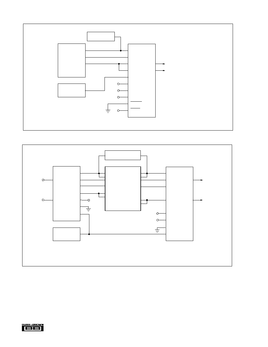
Figure 6 shows a circuit for using the TMS320C25 to
generate a complete analog input and analog output system
using the DSP201 plus the Burr-Brown DSP101 A/D.
Figure 7 shows how to use two TMS320C25 chips to drive
the two channels of the DSP202.
The TMS320C30 has dual serial I/O ports, which can be
used to drive the dual inputs on the DSP202, as shown in
Figure 8. This circuit can maximize the update rate for the
channels. Since the TMS320C30 can also output 32-bit
words, both channels of the DSP202 can be updated from a
single serial output port on the TMS320C30, using the
cascade mode as shown in Figure 9.
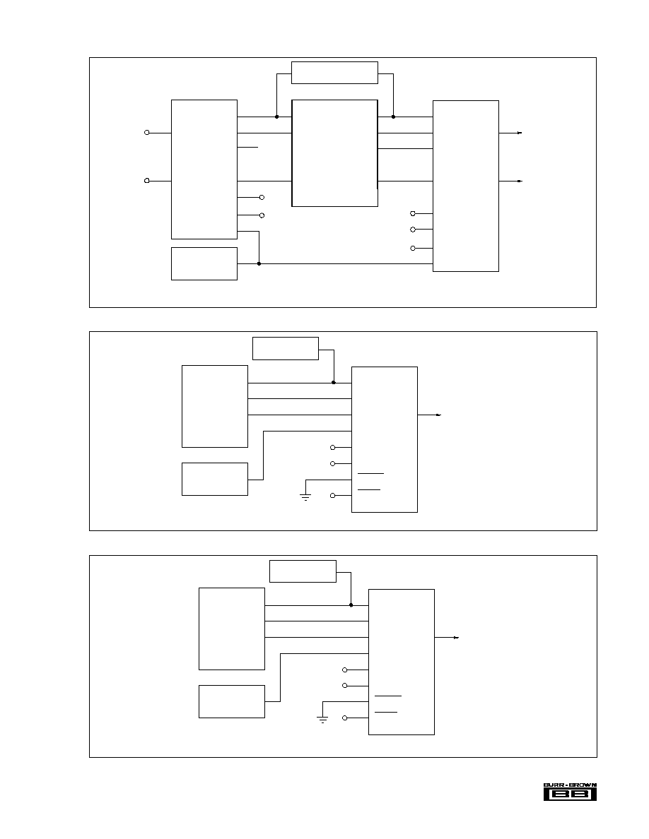
Figures 10 and 11 show complete two-channel analog input
and analog output systems consisting of three basic chips,
the TMS320C30 plus a DSP202 dual D/A and a Burr-
Brown DSP102 dual A/D. Figure 10 makes use of the dual
serial I/O ports on the TMS320C30, and is shown with the
DSP202 in the 16-bit Mode, which maximizes the possible
throughput rate on the system. Figure 11 makes use of the
32-bit word length mode in the TMS320C30 and the Cas-
cade Mode on both the DSP202 and the DSP102 to provide
two full analog I/O channels over a single serial I/O port
on the TMS320C30. Thus, up to four complete, separate
analog I/O channels could be operated using a single
TMS320C30, by making use of the second serial port.
Figure 12 shows how to use a TMS320C25 to update the
analog output of the DSP201.
USING DSP201 AND DSP202
WITH MOTOROLA DSP ICS
Figure 13 shows how to use the DSP201 with a Motorola
DSP56001. Using the DSP202 requires using two
DSP56001s, as indicated in Figure 7.
The DSP56001 needs to be programmed for transmission of
the MSB bit first with SYNC in the Bit Mode. If the
DSP56001 is programmed for 16-bit data words, SWL (pin
10) on the DSP201 or DSP202 needs to be tied HIGH to
select the 16-bit Mode. In the DSP56001 24-bit mode, the
DSP201 or DSP202 can be programmed to accept data
lengths of 16-bits (with SWL HIGH) or 18-bits (with SWL
LOW), and will ignore the trailing bits on the serial line.
For use with the Motorola DSP56001, SSF (pin 9) on the
DSP201 or DSP202 needs to be tied HIGH. This will cause
the DSP201 or DSP202 to transmit an appropriate active
High synchronization pulse on SYNC (pin 11) after a Con-
vert Command is received by the DSP201 or DSP202.
Timing is shown in Figure 1.
Even though the DSP201 or DSP202 require a minimum of
24 Bit Clock pulses between convert commands, the maxi-
mum update rate for the D/As using a 5MHz Bit Clock will
still be over 200kHz (5MHz / 24 = 208.3kHz.)
TTL Bit
Clock
12
13
14
11
9
10
16
15
XCLK
SINA
SINB
SYNC
SSF
SWL
CASC
CONV
±3V Analog Output Channel A
21
VOUTA
VOUTB
DSP202
Conversion Rate
Generator
CLKX - 0
CLKX - 1
TMS320C30
+5V
±3V Analog Output Channel B
5
+5V
DX - 0
DX - 1
FSX - 0
FSX - 1
NOTE: (1) Serial output is 16-bit MSB first.
FIGURE 8. Using DSP202 with TMS320C30's Dual SIO.
Æ
DSP201/202
16
FIGURE 10. Two-Channel Analog Input and Output System with TMS320C30.
TTL Bit
Clock
12
13
14
11
9
10
16
15
XCLK
SINA
SINB
SYNC
SSF
SWL
CASC
CONV
±3V Analog Output
Channel A
21
VOUTA
DSP202
Conversion Rate
Generator
XCLK
SOUTA
SOUTB
SYNC
SSF
CASC
CONV
DSP102*
+5V
+5V
16
20
17
15
12
22
21
2
25
±2.75V
Analog Input
Channel A
DR-0
DR-1
DX-0
DX-1
±2.75V
Analog Input
Channel B
VINA
VINB
TMS320C30
CLKR-0
CLKR-1
FSR-0
FSR-1
CLKR-0
CLKR-1
FSX-0
FSX-1
NOTES: (1) Sample rate on DSP102 and DSP202 may differ. (2) Analog Devices ADSP2101 may be used. SPORT1 and SPORT2
are used for serial MSB first communication.
±3V Analog Output
Channel B
5
VOUTB
+5V
*See Burr-Brown DSP101/102 product data sheet for full description of this ADC.
FIGURE 9. Using DSP202 with TMS320C30 in Cascade Mode.
TTL Bit
Clock
12
11
13
14
15
16
9
10
17
8
XCLK
SYNC
SINA
SINB
CONV
CASC
SSF
SWL
ENABLE
RESET
+5V
±3V Analog Output Channel A
21
VOUTA
VOUTB
DSP202
Conversion Rate
Generator
CLKX
FSX
DX
TMS320C30
+5V
+5V
±3V Analog Output Channel B
5
+5V
NOTE: Program TMS320C30 for 32-bit mode.
Æ
DSP201/202
17
TTL Bit
Clock
12
13
14
11
9
10
16
15
XCLK
SINA
SINB
SYNC
SSF
SWL
CASC
CONV
±3V Analog Output
Channel A
21
VOUTA
DSP202
Conversion Rate
Generator
XCLK
SOUTA
SOUTB
SYNC
SSF
CASC
CONV
DSP102*
+5V
+5V
+5V
16
20
17
15
12
22
21
2
25
±2.75V
Analog Input
Channel A
CLKX-0
DX-0
FSX-0
±2.75V
Analog Input
Channel B
VINA
VINB
TMS320C30
CLKR-0
DR-0
FSR-0
NOTES: (1) Program TMS320C30 for 32-bit mode. (2) Sample rate on DSP102 and DSP202 may differ. (3) DSP32C may also be used
in this mode, with SSF pins tied LOW. *See Burr-Brown DSP101/DSP102 product data sheet for full description of this ADC.
+5V
+5V
NC
±3V Analog Output
Channel B
5
VOUTB
FIGURE 11. Two-Channel Analog Input and Output System with TMS320C30 in Cascade Mode.
FIGURE 12. Using DSP201 with TMS320C25.
FIGURE 13. Using DSP201 with DSP56001.
TTL Bit
Clock
12
11
13
15
9
10
17
8
XCLK
SYNC
SIN
CONV
SSF
SWL
ENABLE
RESET
+5V
+5V
±3V Analog Output
21
VOUT
DSP201
Conversion Rate
Generator
CLKX
FSX
DX
TMS320C25
SSI Port
NOTE: FSX is programmed for external mode.
+5V
TTL Bit
Clock
12
11
13
15
9
10
17
8
XCLK
SYNC
SIN
CONV
SSF
SWL
ENABLE
RESET
+5V
+5V
±3V Analog Output
21
VOUT
DSP201
Conversion Rate
Generator
SSK
SS2
STD
DSP56001
SSI Port
TXC
FSR (Bit)
NOTES: (1) DSP56001 programmed for MSB bit first. (2) For 16-bit data connect SWL to Logic 1; For 24-bit data connect SWL to Logic 0.
(2)
Æ
DSP201/202
18
USING DSP201 AND DSP202 WITH ADI DSP ICS
When using the DSP201 or DSP202 with the ADSP2101 or
ADSP2105, the processors need to be programmed to trans-
mit the data with the MSB first.
Figure 14 shows the connections required to generate an
analog output channel using an ADSP2105 with the DSP201.
The same basic circuit can also be used to connect a DSP201
to the ADSP2101.
Figure 6 indicates how to build a complete analog input and
analog output system using either the ADSP2101 or
ADSP2105 with a DSP201 and a Burr-Brown DSP101 A/D.
The two serial ports on the ADSP2101 can also be used with
the DSP202 to make two complete analog output channels
as noted in footnote 2 of Figure 10.
USING DSP201 AND
DSP202 WITH AT&T DSP ICS
Figures 15, 16 and 17 show how to use the DSP201 and
DSP202 with the DSP16 and DSP32C in different modes.
The DSP IC needs to be programmed to transmit data with
the MSB first, and the DSP201 or DSP202 needs to have
SSF (Select Sync Format on pin 9) tied LOW so that the
FIGURE 14. Using DSP201 with ADSP-2105.
D/As will output an appropriate active Low synchronization
pulse after a Convert Command is received.
Figures 15 and 17 show the DSP32C and DSP16 respec-
tively used with the DSP201 in the 16-bit Mode to generate
a single analog output channel. With a 12MHz Bit Clock and
the 24 Bit Clock cycles required by the DSP201 and DSP202
between Convert Commands, the output of Figure 15 can be
updated at a full 500kHz (12MHz/24 = 500kHz.)
Figure 16 shows how to drive two analog output channels
from a single 32-bit serial port on the DSP32C, using the
Cascade Mode on the DSP202. With a 12MHz Bit Clock
and the 40 Bit Clock cycles required between Convert
Commands by the DSP for internal logic overhead, this
circuit can update two separate analog outputs at 300kHz
each from a single serial port (12MHz/40 = 300kHz.)
Figure 6 indicates how to build a complete analog input and
analog output system using a DSP32C or DSP16 with a
DSP201 and a Burr-Brown DSP101 A/D.
Figure 7 shows a two channel analog output system using a
single DSP202 with two DSP32Cs or two DSP16s.
TTL Bit
Clock
12
13
11
9
10
15
XCLK
SIN
SYNC
SSF
SWL
CONV
±3V Analog Output
21
VOUT
DSP201
Conversion Rate
Generator
SCLK1
DT1
(1)
ADSP2105
NOTE: (1) 16-bit MSB first data.
+5V
+5V
TFS1

Æ
DSP201/202
19
FIGURE 17. Using DSP201 with DSP16.
TTL Bit
Clock
12
11
13
15
9
10
17
8
XCLK
SYNC
SIN
CONV
SSF
SWL
ENABLE
RESET
+5V
±3V Analog Output
21
VOUT
DSP201
Conversion Rate
Generator
OCK
OLD
DO
OEN
DSP32C
NOTES: DSP32C programmed for MSB bit first. Data length 16 bit. External OCK, ILD.
+5V
SIO
FIGURE 15. Using DSP201 with DSP32C with 16-Bit Data Words.
TTL Bit
Clock
12
11
13
14
15
16
9
10
17
8
XCLK
SYNC
SINA
SINB
CONV
CASC
SSF
SWL
ENABLE
RESET
+5V
±3V Analog Output Channel A
21
VOUTA
VOUTB
DSP202
Conversion Rate
Generator
OCK
OLD
DO
OEN
DSP32C
+5V
+5V
±3V Analog Output Channel B
5
SIO
NOTES: (1) DSP32C programmed for MSB bit first. (2) Data length 32 bits. External OCK, ILD.
FIGURE 16. Using DSP202 with DSP32C in Cascade Mode.
TTL Bit
Clock
12
11
13
9
10
15
XCLK
SYNC
SIN
SSF
SWL
CONV
±3V Analog Output
21
VOUT
DSP201
Conversion Rate
Generator
OCK
OLD
DO
OEN
DSP16
NOTE: (1) DSP16 programmed for MSB bit first 16-bit data.
+5V
SIO