 | –≠–ª–µ–∫—Ç—Ä–æ–Ω–Ω—ã–π –∫–æ–º–ø–æ–Ω–µ–Ω—Ç: ISO213 | –°–∫–∞—á–∞—Ç—å:  PDF PDF  ZIP ZIP |
ISO213
International Airport Industrial Park ∑ Mailing Address: PO Box 11400 ∑ Tucson, AZ 85734 ∑ Street Address: 6730 S. Tucson Blvd. ∑ Tucson, AZ 85706
Tel: (520) 746-1111 ∑ Twx: 910-952-1111 ∑ Cable: BBRCORP ∑ Telex: 066-6491 ∑ FAX: (520) 889-1510 ∑ Immediate Product Info: (800) 548-6132
PDS-881E
Two-Port Isolated, Low Profile
ISOLATED INSTRUMENTATION AMPLIFIER
FEATURES
q
GAIN RANGE: 0.5 - 5000
q
±
10V INPUT SIGNAL RANGE
q
INSTRUMENTATION AMPLIFIER INPUTS
q
±
40V INPUT OVER VOLTAGE
PROTECTION
q
12-BIT ACCURACY
q
LOW PROFILE (Less Than 0.5" High)
q
SMALL FOOTPRINT
q
EXTERNAL POWER CAPABILITY
(
±
14V at 3mA)
q
SYNCHRONIZATION CAPABILITY
q
SINGLE 12V TO 15V SUPPLY OPERATION
q
LOW POWER (45mW)
APPLICATIONS
q
INDUSTRIAL PROCESS CONTROL:
Transducer Channel Isolator for
Thermocouples, RTDs, Pressure
Bridges, Flow Meters
q
4mA TO 20mA LOOP ISOLATION
q
MOTOR AND SCR CONTROL
q
GROUND LOOP ELIMINATION
q
ANALYTICAL MEASUREMENTS
q
POWER PLANT MONITORING
q
DATA ACQUISITION/TEST EQUIPMENT
ISOLATION
q
MULTIPLEXED SYSTEMS WITH
CHANNEL TO CHANNEL ISOLATION
ISO213
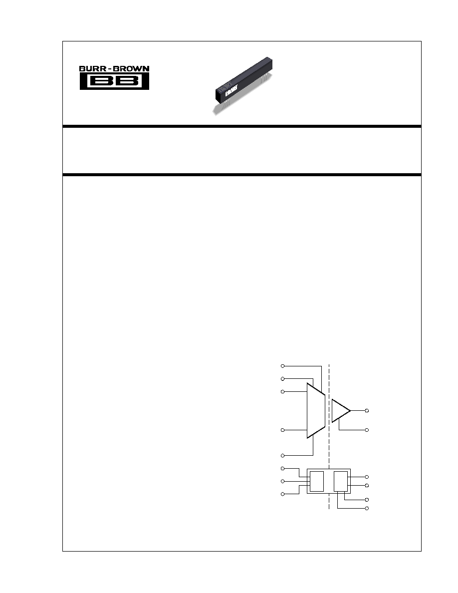
DESCRIPTION
ISO213 signal isolation amplifier is a member of a
series of low-cost isolation products from Burr-Brown.
The low-profile ZIP plastic package allows PCB spac-
ings of 0.5" to be achieved, and the small footprint
results in efficient use of board space.
To provide isolation, the design uses high-efficiency,
miniature toroidal transformers in both the signal and
power paths. An uncommitted instrumentation ampli-
fier on the input and an isolated external bipolar supply
ensure the majority of input interfacing or conditioning
needs can be met.
Gain
Set
8
7
≠V
IN
3
+V
IN
1
F
B
4
6
Com 1
2
5
38
37
ACom 2
Isolation Barrier
+V
SS
Out
Com 2
+V
V
OUT
CC
Clock Out
Clock In
DC/DC
Converter
≠V
SS
Out
31
32
34
35
Æ
©
1995 Burr-Brown Corporation
PDS-1281A
Printed in U.S.A. April, 1995
2
Æ
ISO213
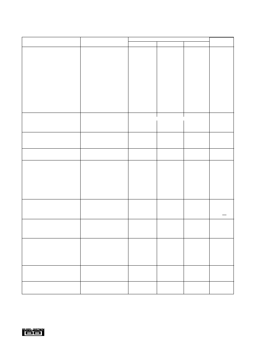
PARAMETER
CONDITIONS
MIN
TYP
MAX
UNITS
ISOLATION
Voltage
Rated Continuous
AC, 50/60Hz
1500
Vrms
DC
2120
VDC
Rated 1 min
AC, 50/60Hz
2500
Vrms
100% Test (AC, 50Hz)
Partial Discharge
2500
Vrms
1s <5pC
Isolation-Mode Rejection
(1)
V
ISO
= Rated
Continuous 50/60Hz
AC
115
dB
DC
160
dB
Barrier Resistance
10
10
Barrier Capacitance
15
pF
Leakage Current
(2)
V
ISO
= 240Vrms, 60Hz
3
µ
Arms
V
ISO
= 240Vrms, 50Hz
2.4
µ
Arms
GAIN
Equation
Initial Error
G = 0.5
±
0.2
±
3
% FSR
(8)
Gain vs Temperature
G = 0.5
10
50
ppm of FSR/
∞
C
Non-Linearity
(3)
V
O
= ≠5V to +5V, G = 0.5
0.01
0.025
%FSR
INPUT OFFSET VOLTAGE
Offset Voltage RTI
±
0.5
±
25/G
mV
vs Temperature
±
5
±
35/G
µ
V/
∞
C
vs Power Supply
(4)
G = 0.5,V
CC
= 14V to 16V
±
3
mV/V
INPUT CURRENT
Bias
±
1
±
10
nA
Offset
±
1
±
10
nA
INPUT
Linear Input Range
(5)
G = 0.5
±
10
±
12
V
Common-Mode Rejection
V
CM
=
±
10V,
R
S
= 1k
G = 0.5
73
90
dB
G = 5
89
110
dB
G = 50
98
120
dB
G = 500
100
125
dB
Impedance
Differential
10
10
|| 3
|| pF
Common-Mode
10
10
|| 6
|| pF
OUTPUT
Output Impedance
3
k
Voltage
Load = 1M
±
5
V
Ripple Voltage
(6)
f = clk
1
mVp-p
Output Noise
f = 0 to 5kHz
20
µ
V/
Hz
FREQUENCY RESPONSE
Small Signal Bandwidth
V
IN
= 1Vp-p, ≠3dB,
1
kHz
G = 0.5
Full Signal Bandwidth
V
IN
= 10Vp-p, ≠3dB,
200
Hz
G = 0.5
ISOLATED POWER OUTPUTS
Voltage Outputs (
±
V
SS
)
(7)
3mA
±
13
±
14
VDC
vs Temperature
7
mV/
∞
C
vs Load
180
mV/mA
Current Output
(7)
(Both Loaded)
V
SS
=
±
13V
3
6
mA
(One Loaded)
V
SS
=
±
13V
4
6
mA
POWER SUPPLIES
Rated Voltage
Rated Performance
15
V
Voltage Range
(5, 9)
11.4 to 16
V
Quiescent Current
No Load
3
6
mA
TEMPERATURE RANGE
Specification
0
+70
∞
C
Operating
≠25
+85
∞
C
NOTES: (1) Isolation-mode rejection is the ratio of the change in output voltage to a change in isolation barrier voltage. (2) Tested at 2500Vrms 50Hz limit 25
µ
A (barrier
is essentially capacitive). (3) Nonlinearity is the peak deviation of the output voltage from the best-fit straight line. It is expressed as the ratio of deviation to FSR.
(4) Power Supply Rejection is the change in V
OS
/Supply Change. (5) See max V
OUT
and V
IN
vs Supply Voltage in typical performance curves. (6) Ripple is the residual
component of the barrier carrier frequency generated internally. (7) Derated at V
CC
< 15V. (8) FSR = Full Scale Output Range = 10V. (9) Minimum supply voltage
is given as 11.4V. This is the minimum supply to ensure a
±
5V output swing can be achieved. The ISO213 actually works down to a minimum supply of 4V as shown
in the typical performance curve "Max V
OUT
and V
IN
vs Supply Voltage."
SPECIFICATIONS
At T
A
= +25
∞
C, V
CC
= +15V, unless otherwise noted.
ISO213P
G = (1 + 50k/R
G
)/2
3
Æ
ISO213
ABSOLUTE MAXIMUM RATINGS
Supply Voltage Without Damage ......................................................... 18V
Continuous Isolation Voltage Across Barrier: ............................ 2500Vr ms
Storage Temperature Range ............................................ ≠25
∞
C to 100
∞
C
Lead Temperature (soldering, 10s) ............................................... +300
∞
C
Amplifier Output Short-Circuit Duration ............... Continuous to Common
Output Voltage to Com 2 ...............................................................
±
V
CC
/2
MODEL
PACKAGE
RANGE
RATING 1 MIN
ISO213P
38-Pin Plastic ZIP
≠25
∞
C to +85
∞
C
2500Vr ms
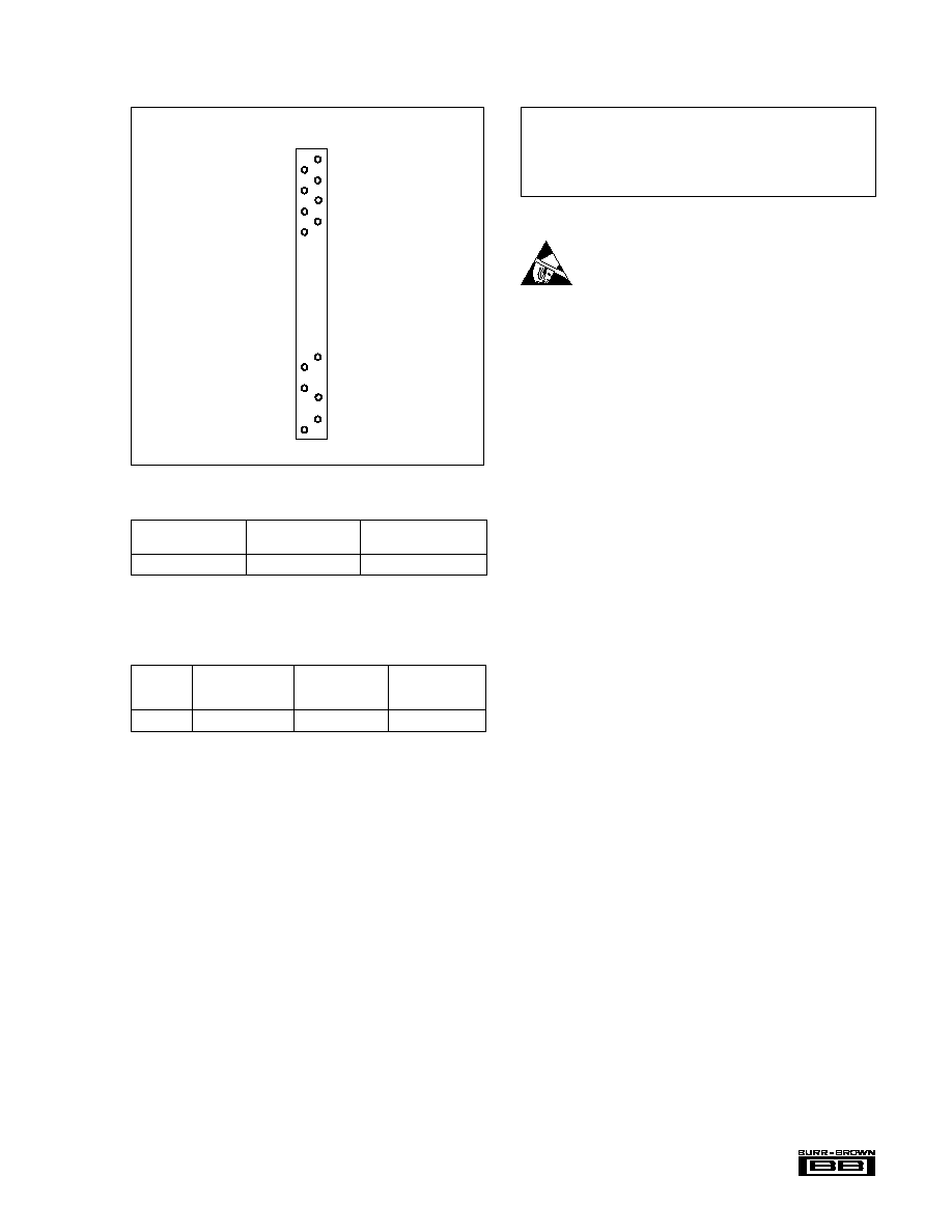
Bottom View
Com 1 2
F
B
4
+V
SS
6
GS
A
8
The information provided herein is believed to be reliable; however, BURR-BROWN assumes no responsibility for inaccuracies or omissions. BURR-BROWN assumes
no responsibility for the use of this information, and all use of such information shall be entirely at the user's own risk. Prices and specifications are subject to change
without notice. No patent rights or licenses to any of the circuits described herein are implied or granted to any third party. BURR-BROWN does not authorize or warrant
any BURR-BROWN product for use in life support devices and/or systems.
1 +V
IN
3 ≠V
IN
5 ≠V
SS
7 GS
B
31 +V
CC
35 Clock In
37 ACom 2
PIN CONFIGURATION
PACKAGE INFORMATION
PACKAGE DRAWING
MODEL
PACKAGE
NUMBER
(1)
ISO213P
38-Pin Plastic ZIP
326
NOTE: (1) For detailed drawing and dimension table, please see end of data
sheet, or Appendix D of Burr-Brown IC Data Book.
ORDERING INFORMATION
OPERATING
TEMPERATURE
ISOLATION
ELECTROSTATIC
DISCHARGE SENSITIVITY
This integrated circuit can be damaged by ESD. Burr-Brown
recommends that all integrated circuits be handled with
appropriate precautions. Failure to observe proper handling
and installation procedures can cause damage.
ESD damage can range from subtle performance degradation
to complete device failure. Precision integrated circuits may
be more susceptible to damage because very small parametric
changes could cause the device not to meet its published
specifications.
Com 2 32
Clock Out 34
V
OUT
38
4
Æ
ISO213
IMR vs FREQUENCY
1k
10k
100k
1M
10M
85
80
75
70
65
60
55
50
45
40
Frequency (Hz)
IMR (dB)
100M
MAX V
OUT
AND V
IN
vs SUPPLY VOLTAGE
2
15
10
5
0
≠5
≠10
≠15
Supply Voltage
Maximum Input Voltage
0
≠5
5
10
≠10
Maximum Output Voltage
4
6
8
10
12
14
≠V
OUT
+V
OUT
+V
IN
≠V
IN
±V
OUT
+
≠
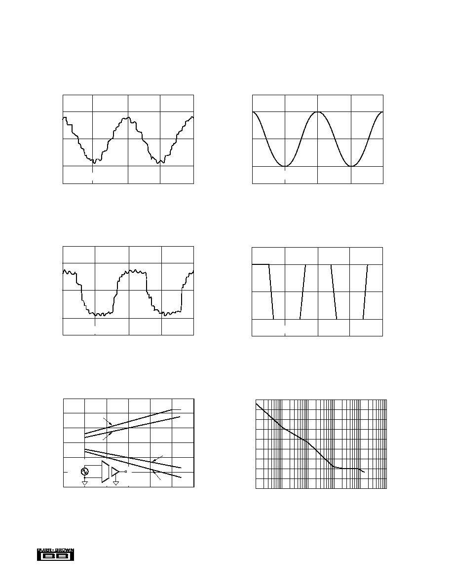
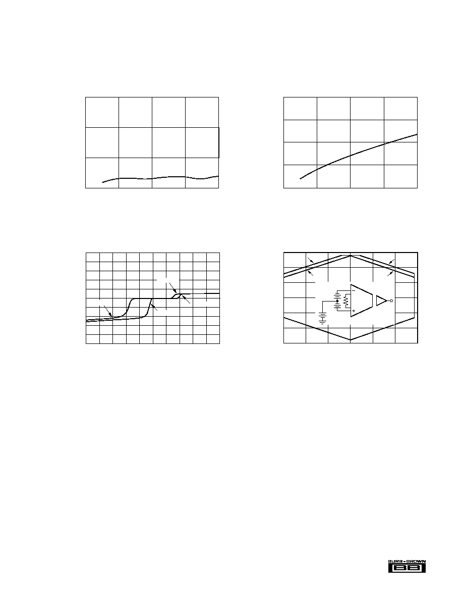
STEP RESPONSE (f = 200Hz)
Output Voltage (V)
+5
0
≠5
0
5
10
Time (ms)
V = ±10V, G = 0.5
IN
STEP RESPONSE (f = 2kHz)
0
500
1000
Time (µs)
Output Voltage (mV)
+500
0
≠500
V = ±1V, G = 0.5
IN
SINE RESPONSE (f = 200Hz)
0
+5
Time (ms)
Output Voltage (V)
0
≠5
5
10
V
IN
= ±10V, G = 0.5
SINE RESPONSE (f = 2kHz)
Output Voltage (mV)
+500
0
≠500
0
500
1000
Time (µs)
V = ±1V, G = 0.5
IN
TYPICAL PERFORMANCE CURVES
At T
A
= +25
∞
C, V
CC
= +15V, unless otherwise noted.
5
Æ
ISO213
INPUT COMMON-MODE RANGE
vs OUTPUT VOLTAGE
Output Voltage (V)
Common-Mode Voltage (V)
≠7.5
≠5
0
2.5
7.5
≠2.5
15
10
5
0
≠5
≠10
≠15
5
All
Gains
All
Gains
G = 0.5
G = 0.5
G
5
G
5
V
D/2
≠
+
≠
+
V
CM
V
OUT
V
D/2
ISO213P
INPUT BIAS CURRENT
vs INPUT OVERLOAD VOLTAGE
10
8
6
4
2
0
≠2
≠4
≠6
≠8
≠10
Input Bias Current (mA)
Overload Voltage (V)
≠40
0
40
G = 0.5
G = 500
G = 0.5
G = 500
0.4
0.3
0.2
0.1
0
30
40
60
80
100
GAIN ERROR vs CLOCK RATE
Clock (kHz)
Gain Error (%)
NON-LINEARITY vs CLOCK RATE
20
40
60
80
100
Clock (kHz)
30
20
10
0
Non-Linearity (m%)
TYPICAL PERFORMANCE CURVES
(CONT)
At T
A
= +25
∞
C, V
CC
= +15V, unless otherwise noted.