 | ÐлекÑÑоннÑй компоненÑ: ISO253 | СкаÑаÑÑ:  PDF PDF  ZIP ZIP |
Äîêóìåíòàöèÿ è îïèñàíèÿ www.docs.chipfind.ru
©
1996 Burr-Brown Corporation
PDS-1310B
Printed in U.S.A. April, 1996
International Airport Industrial Park · Mailing Address: PO Box 11400 · Tucson, AZ 85734 · Street Address: 6730 S. Tucson Blvd. · Tucson, AZ 85706
Tel: (520) 746-1111 · Twx: 910-952-1111 · Cable: BBRCORP · Telex: 066-6491 · FAX: (520) 889-1510 · Immediate Product Info: (800) 548-6132
®
Precision, Powered, Three-Port Isolated
BUFFER AMPLIFIER
DESCRIPTION
ISO253 is a precision three-port isolated buffer ampli-
fier incorporating a novel duty cycle modulation-
demodulation technique and has excellent accuracy.
The input is protected to withstand
±
100V without
damage. The signal is transmitted digitally across a
differential capacitive barrier. With digital modulation
the barrier characteristics do not affect signal integrity.
This results in excellent reliability and good high
frequency transient immunity across the barrier. The
DC/DC converter, amplifier and barrier capacitors are
housed in a plastic DIP.
This amplifier is easy to use as no external compo-
nents are required. A power supply range of 11V to
18V makes this amplifier ideal for a wide range of
applications.
ISO253
FEATURES
q
RATED
1500Vrms Continuous
2500Vrms for One Minute
q
100% TESTED FOR PARTIAL DISCHARGE
q
LOW NONLINEARITY:
±
0.01% typ
q
INPUT PROTECTED TO
±
100V
q
BIPOLAR OPERATION: V
O
=
±
10V
q
SYNCHRONIZATION CAPABILITY
q
28-PIN PLASTIC DIP: 0.6" Wide
ISO253
+V
S1
Com1
+V
IN
V
S1
GND1
28
26
1
27
25
+V
S2
Com2
V
S2
GND2
12
V
OUT
14
13
11
10
ISO253
BUF
17
GND3
16
SYNC
15
+V
S3
APPLICATIONS
q
INDUSTRIAL PROCESS CONTROL
Transducer Isolator, Thermocouple
Isolator, RTD Isolator, Pressure Bridge
Isolator, Flow Meter Isolator
q
POWER MONITORING
q
MEDICAL INSTRUMENTATION
q
ANALYTICAL MEASUREMENTS
q
DATA ACQUISITION
q
TEST EQUIPMENT
q
GROUND LOOP ELIMINATION

2
®
ISO253
ISO253P
PARAMETER
CONDITIONS
MIN
TYP
MAX
UNITS
ISOLATION
Voltage Rated Continuous:
AC
T
MIN
to T
MAX
1500
Vrms
100% Test (AC 50Hz)
1s; Partial Discharge
5pC
2500
Vrms
Rated One Min
2500
Vrms
Isolation-Mode Rejection
DC
120
dB
AC 50Hz
1500Vrms
95
dB
Barrier Impedance
10
14
|| 2
|| pF
Leakage Current
VISO = 240Vrms, 50Hz
1.4
2
µ
Arms
GAIN
Nominal Gain
1
V/V
Gain Error
0.15
±
0.3
%
Gain vs Temperature
15
ppm/
°
C
Nonlinearity
0.01
±
0.1
%
INPUT OFFSET VOLTAGE
Initial Offset
±
100
mV
vs Temperature
150
µ
V/
°
C
vs Supply
1
mV/V
INPUT
Voltage Range
±
10
±
15
V
Resistance
200
k
OUTPUT
Voltage Range
±
10
V
Current Drive
±
5
mA
Capacitive Load Drive
0.1
µ
F
Ripple Voltage
25
mVp-p
FREQUENCY RESPONSE
Small Signal Bandwidth
50
kHz
Slew Rate
0.25
V/
µ
s
Settling Time, 0.1%
50
µ
s
POWER SUPPLIES
Rated Voltage
15
V
Voltage Range
11
18
V
Quiescent Current
25
40
55
mA
Rated Output Voltage
No Load
13
14.5
V
50mA Load On Two Supplies
12
13.2
16
V
Load Regulation
28
mV/mA
Line Regulation
1
V/V
SYNC Frequency
1
1.4
MHz
Output Voltage Ripple
50
mV
TEMPERATURE RANGE
Operating
40
85
°
C
Storage
40
85
°
C
SPECIFICATIONS
At T
A
= +25
°
C, V
S3
= 15V, R
L
= 2k
, and 220nF capacitors on all generated supplies, unless otherwise noted.
3
®
ISO253
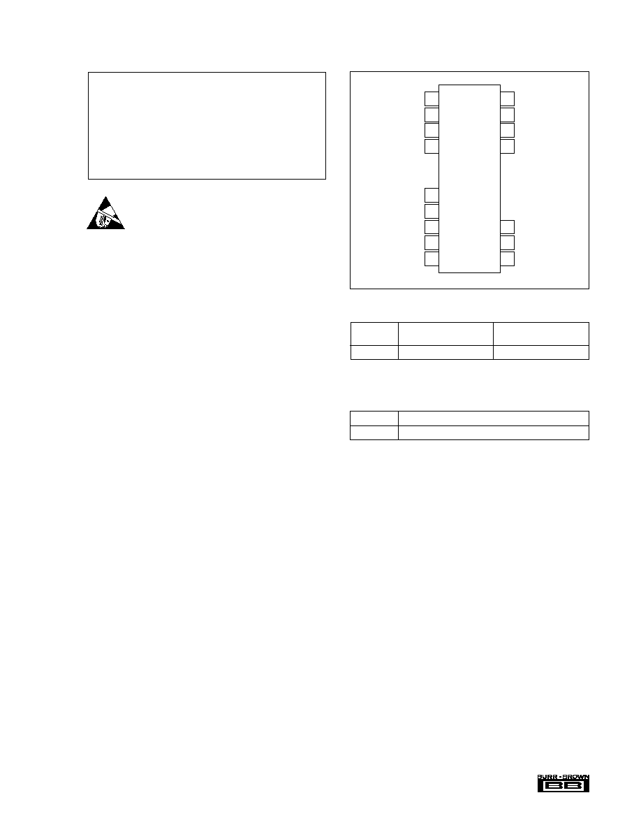
PIN CONFIGURATION
Any integrated circuit can be damaged by ESD. Burr-Brown
recommends that all integrated circuits be handled with
appropriate precautions. Failure to observe proper handling
and installation procedures can cause damage.
ESD damage can range from subtle performance degrada-
tion to complete device failure. Precision integrated circuits
may be more susceptible to damage because very small
parametric changes could cause the device not to meet
published specifications.
PACKAGE INFORMATION
PACKAGE DRAWING
PRODUCT
PACKAGE
NUMBER
(1)
ISO253P
28-Pin Plastic DIP
335
NOTE: (1) For detailed drawing and dimension table, please see end of data
sheet, or Appendix C of Burr-Brown IC Data Book.
ELECTROSTATIC
DISCHARGE SENSITIVITY
ABSOLUTE MAXIMUM RATINGS
Supply Voltage ................................................................................... +18V
V
IN
, Analog Input Voltage Range .....................................................
±
100V
Com1 to GND1 ....................................................................................
±
1V
Com2 to GND2 ....................................................................................
±
1V
Continuous Isolation Voltage: .................................................... 1500Vrms
..................................................................................... 2500Vrms one min
IMV, dv/dt ...................................................................................... 20kV/
µ
s
Junction Temperature ...................................................................... 150
°
C
Storage Temperature ........................................................ 40
°
C to +85
°
C
Lead Temperature (soldering, 10s) ................................................ +300
°
C
Output Short Duration .......................................... Continuous to Common
NC
NC
+V
S2
V
S2
GND2
Com2
V
OUT
Com1
GND1
GND3
SYNC
+V
S3
NC
V
S1
+V
IN
1
2
3
4
10
11
12
13
14
28
27
26
25
17
16
15
+V
S1
ORDERING INFORMATION
PRODUCT
PACKAGE
ISO253P
28-Pin Plastic DIP
The information provided herein is believed to be reliable; however, BURR-BROWN assumes no responsibility for inaccuracies or omissions. BURR-BROWN assumes
no responsibility for the use of this information, and all use of such information shall be entirely at the user's own risk. Prices and specifications are subject to change
without notice. No patent rights or licenses to any of the circuits described herein are implied or granted to any third party. BURR-BROWN does not authorize or warrant
any BURR-BROWN product for use in life support devices and/or systems.
4
®
ISO253
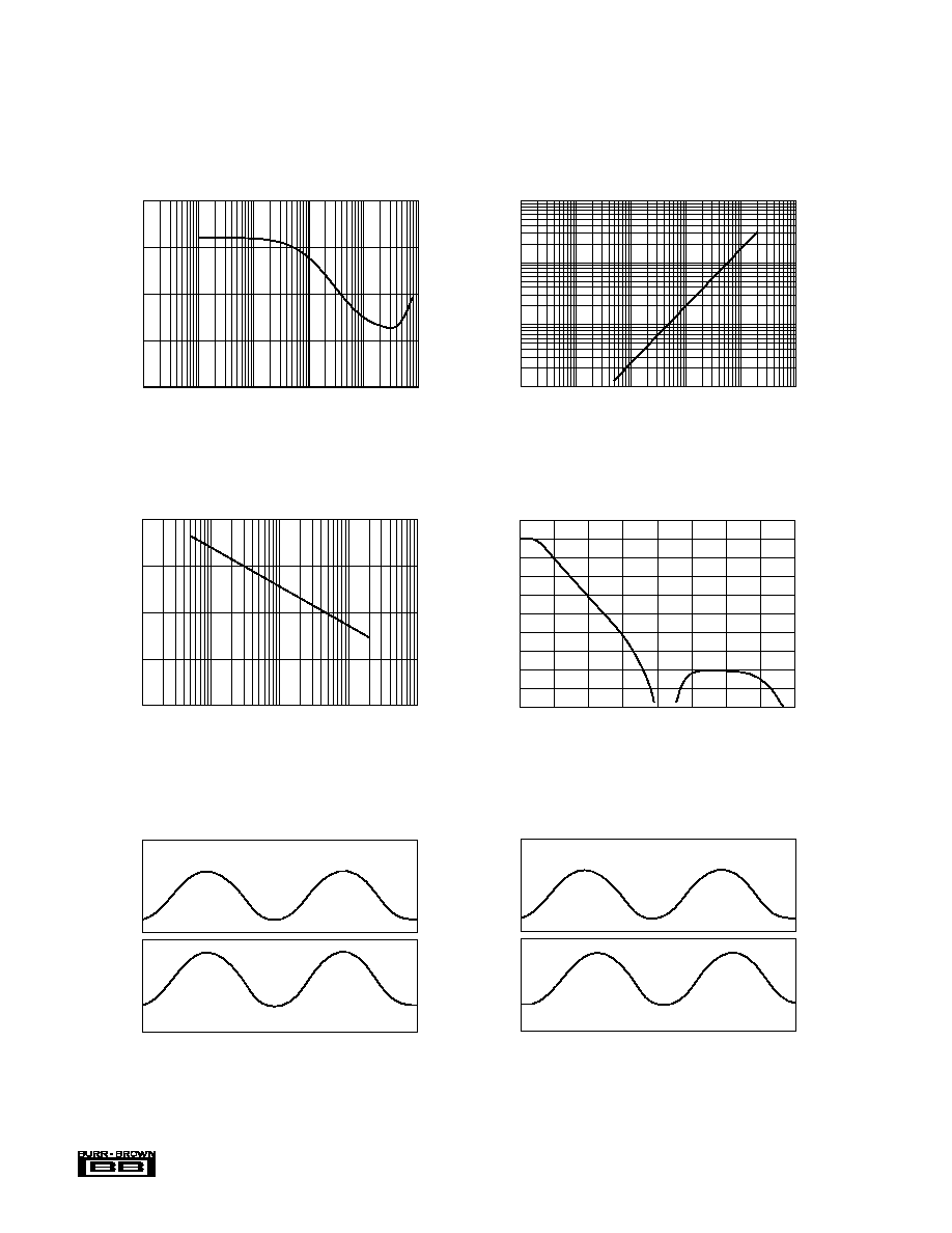
TYPICAL PERFORMANCE CURVES
At T
A
= +25
°
C, +V
S3
= 15V, R
L
= 2k
, and 220nF capacitors on all generated supplies, unless otherwise noted.
0
Frequency (Hz)
10
0
10
20
30
40
50
60
70
80
90
Signal (dB)
800k
100k
200k
300k
400k
500k
600k
700k
SIGNAL RESPONSE vs CARRIER FREQUENCY
1
Frequency (Hz)
80
60
40
20
0
PSRR (dB)
PSRR vs FREQUENCY
100
100K
10
1K
10K
1
Frequency (Hz)
1k
100
10
1
µ
Amps (rms)
ISOLATION LEAKAGE CURRENT vs FREQUENCY
(V = 240Vrms)
100
100k
10
1k
10k
1
Frequency (Hz)
120
100
80
60
40
Rejection (dB)
10k
10
100
1k
IMR vs FREQUENCY
SINE RESPONSE
(f = 1kHz)
10
5
0
5
5
0
5
10
Output (V)
Input (V)
Time (µs)
0
500
1000
1500
2000
SINE RESPONSE
(f = 10kHz)
10
5
0
5
5
0
5
10
Output (V)
Input (V)
0
50
100
150
200
Time (µs)
5
®
ISO253
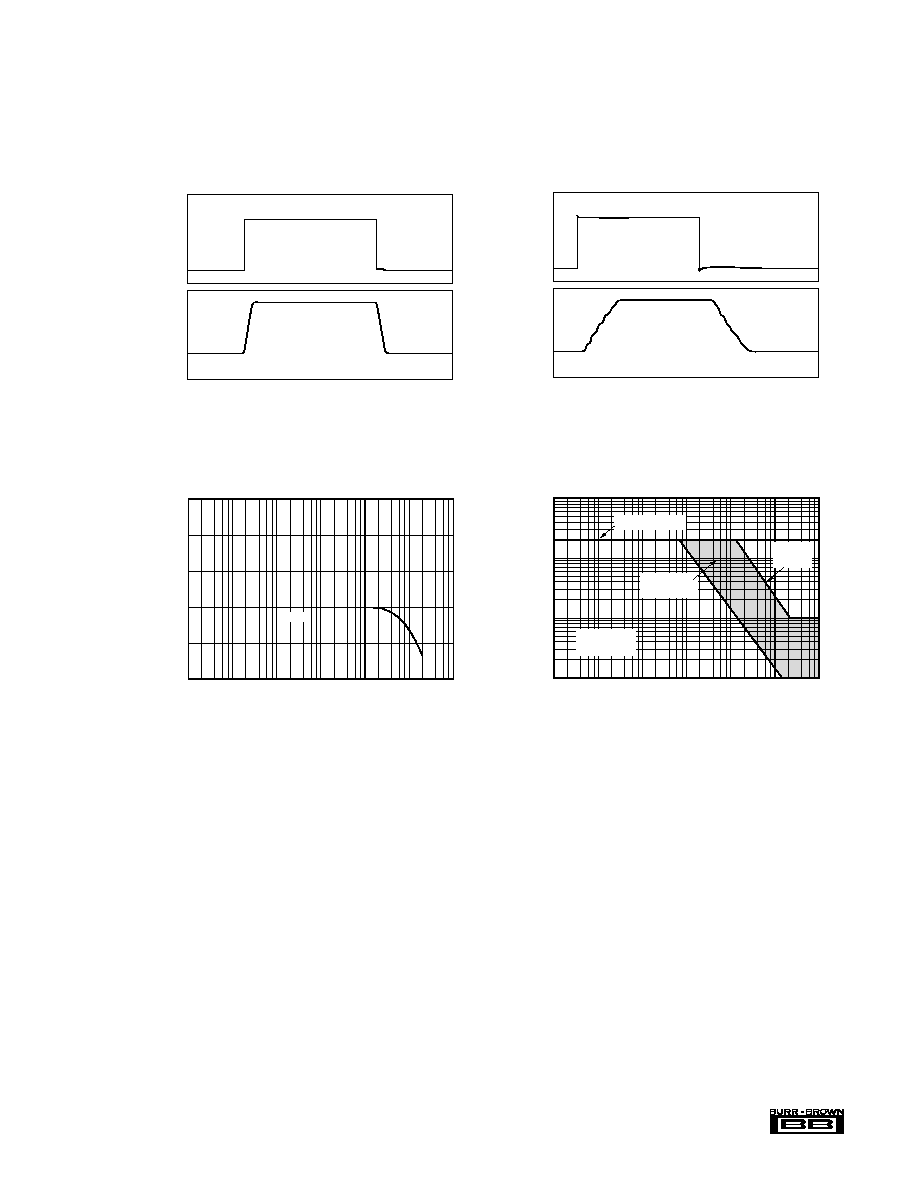
TYPICAL PERFORMANCE CURVES
(CONT)
At T
A
= +25
°
C, +V
S3
= 15V, R
L
= 2k
, and 220nF capacitors on all generated supplies, unless otherwise noted.
GAIN vs FREQUENCY
60
40
20
0
20
40
Gain (dB)
Frequency (Hz)
1
10
100
1k
10k
100k
1M
G = 1
100
Frequency (Hz)
10
1.0k
100
Peak Isolation Voltage
ISOLATION MODE VOLTAGE
vs FREQUENCY
10k
1M
100M
1k
100k
10M
2.1k
Max AC
Rating
Degraded
Performance
Max DC Rating
Typical
Performance
PULSE RESPONSE
(f = 1kHz)
10
5
0
5
5
0
5
10
Output (V)
Input (V)
0
500
1000
Time (µs)
PULSE RESPONSE
(f = 10kHz)
1
1
1
1
Output (V)
Input (V)
0
80
20
40
60
100
Time (µs)